Next Generation Memory Market Size and Share
Market Overview
| Study Period | 2020 - 2031 |
|---|---|
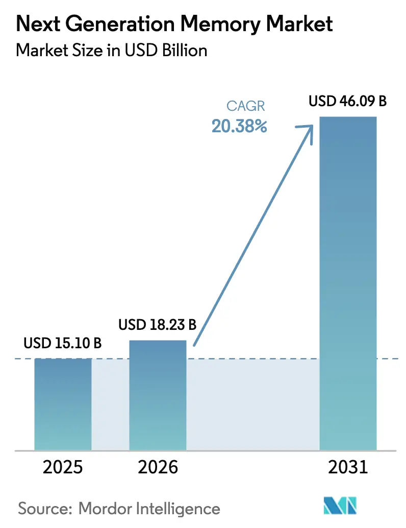
| Market Size (2026) | USD 18.23 Billion |
| Market Size (2031) | USD 46.09 Billion |
| Growth Rate (2026 - 2031) | 20.38% CAGR |
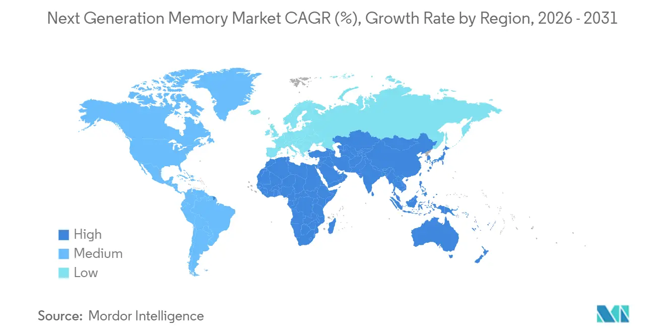
| Fastest Growing Market | Middle East |
| Largest Market | Asia Pacific |
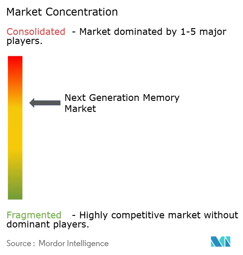
| Market Concentration | Medium |
Major Players *Disclaimer: Major Players sorted in no particular order Image © Mordor Intelligence. Reuse requires attribution under CC BY 4.0. | |
Next Generation Memory Market Analysis by Mordor Intelligence
The next-generation memory market size is projected to expand from USD 15.10 billion in 2025 and USD 18.23 billion in 2026 to USD 46.09 billion by 2031, registering a CAGR of 20.38% between 2026 to 2031. Growing reliance on large-language-model inference, autonomous-driving controllers, and edge analytics nodes is pushing device makers to replace legacy DRAM and NAND with persistent, low-latency storage and compute solutions. Hyperscale operators are inflating per-server memory content as HBM3E becomes the standard stack for AI accelerators, while automotive Tier 1 suppliers are shifting to spin-transfer-torque MRAM for instant-on boot sequences in Level 4 platforms. Capital spending on memory fabs accelerated in 2025 as governments released subsidy tranches tied to supply-chain resilience, and packaging houses invested in through-silicon-via capacity to ease HBM bottlenecks. Collectively, these forces are anchoring the next-generation memory market on a rapid growth trajectory, even amid cyclical softness in consumer electronics demand.
Key Report Takeaways
- By technology, High Bandwidth Memory led with 41.21% revenue share in 2025, while Spin-Transfer-Torque MRAM is forecast to advance at a 23.03% CAGR through 2031.
- By memory interface, DDR and LPDDR commanded 46.51% in 2025; Compute Express Link is set to expand at 22.16% on the back of server-class memory pooling.
- By end-use device, enterprise storage and data centers represented 38.23% in 2025, yet automotive electronics and ADAS will grow at 23.86% as ISO 26262 compliance intensifies.
- By wafer size, 300 millimeter platforms held 67.29% in 2025, while 450 millimeter lines are forecast to progress at 21.44% once lithography hurdles ease.
- By geography, Asia-Pacific accounted for 56.43% of revenue in 2025; the Middle East is projected to climb at 21.65% through 2031 as sovereign AI programs scale.
Note: Market size and forecast figures in this report are generated using Mordor Intelligence’s proprietary estimation framework, updated with the latest available data and insights as of January 2026.
Global Next Generation Memory Market Trends and Insights
Drivers Impact Analysis*
| Driver | (~) % Impact on CAGR Forecast | Geographic Relevance | Impact Timeline |
|---|---|---|---|
| AI-Driven Demand for HBM in Hyperscale Data Centers | +6.2% | Global, concentrated in North America and Asia-Pacific | Short term (≤ 2 years) |
| Automotive L4 ADAS Need for Instant-On Persistent Memory | +4.8% | North America, Europe, China, Japan | Medium term (2-4 years) |
| Smartphone Migration to LPDDR5X and Embedded ReRAM | +3.5% | Asia-Pacific core, spillover to Europe and North America | Short term (≤ 2 years) |
| National Memory Localization Programs | +2.9% | United States, South Korea, China, India, European Union | Long term (≥ 4 years) |
| Industrial Edge-IoT Requiring Ultra-Low-Power FRAM | +1.7% | Global, early adoption in Europe and Japan | Medium term (2-4 years) |
| Data-Privacy-Driven Persistent In-Memory Databases Using 3D XPoint | +1.3% | North America, European Union, Middle East | Long term (≥ 4 years) |
| Source: Mordor Intelligence | |||
AI-Driven Demand for HBM in Hyperscale Data Centers
Generative-AI clusters are breaching GDDR6 bandwidth ceilings, and hyperscalers have moved to HBM3E stacks that deliver up to 819 GB/s per package. SK Hynix began mass production of 12-layer HBM3E in 2024, yet advanced-packaging capacity at leading outsourced assembly houses remains fully booked through mid-2026. NVIDIA’s Blackwell and AMD’s MI300 lines each integrate eight HBM3E stacks, lifting per-accelerator memory content to 192 GB. Power savings of up to 40% versus discrete GDDR modules support data-center sustainability pledges, reinforcing HBM adoption momentum. The consequence is a 6.2-point uplift to the overall CAGR of the next generation memory market.
Automotive L4 ADAS Need for Instant-On Persistent Memory
Level 4 autonomy specifications cap system-start latency at 100 ms, a target unreachable with NAND-based boot paths. STT-MRAM delivers DRAM-like read speed with non-volatility, enabling controllers to resume sensor fusion instantly. Everspin shipped more than 1 million automotive-qualified MRAM units in 2025, and STMicroelectronics entered volume production of 28 nm embedded PCM for 2026 vehicles. Regulatory frameworks such as UNECE WP.29 strengthen the business case by requiring tamper-proof logging. These forces add 4.8 points to the CAGR of the next generation memory market.
Smartphone Migration to LPDDR5X and Embedded ReRAM
In late 2024, Samsung kicked off mass production of its 16 GB LPDDR5X, which boasts a significant 33% power reduction compared to its predecessor, LPDDR5. This advancement highlights Samsung's commitment to enhancing energy efficiency in memory technology. Meanwhile, embedded ReRAM, now in volume production, is being utilized in biometric authentication modules.[1]Samsung Electronics, “Samsung Starts Mass Producing Industry’s First LPDDR5X DRAM,” samsung.com This technology delivers an impressive 10 million-cycle endurance without any erase penalties, making it a reliable choice for high-performance applications. Flagship handsets are now leveraging LPDDR5X, enabling on-device LLM inference speeds to exceed 8,500 MT/s, which is a notable milestone in mobile device performance. Original-equipment makers in the Asia-Pacific region are leading the charge as early adopters of these technologies, driving a notable 3.5-point boost to the market's CAGR and setting the stage for further innovation in the industry.
National Memory Localization Programs
In response to ongoing supply-chain disruptions, a significant wave of subsidies has emerged across the semiconductor industry. Micron, under the CHIPS and Science Act, secured a substantial USD 6.1 billion funding package to construct a state-of-the-art 55,700 m² cleanroom facility in New York, with the project scheduled for completion in 2028. At the same time, South Korea introduced a massive KRW 26 trillion (USD 19 billion) support package aimed at bolstering the development of HBM pilot lines, which are critical for advancing memory technologies. Additionally, China’s "Big Fund III" is strategically channeling significant capital investments into STT-MRAM and ReRAM foundries, further strengthening its position in the global semiconductor market.
Restraints Impact Analysis*
| Restraint | (~) % Impact on CAGR Forecast | Geographic Relevance | Impact Timeline |
|---|---|---|---|
| 450 mm Wafer Delay Constraining ReRAM Scale-Up | -2.1% | Global, acute in Asia-Pacific and Europe | Long term (≥ 4 years) |
| High Per-Bit MRAM Cost Versus NAND | -1.8% | Global | Medium term (2-4 years) |
| Thermal Stability Failures of Automotive-Grade PCM | -0.9% | North America, Europe, China, Japan | Short term (≤ 2 years) |
| Foundry Concentration for Sub-28 nm STT-MRAM | -0.7% | Global, concentrated in Taiwan and South Korea | Medium term (2-4 years) |
| Source: Mordor Intelligence | |||
450 mm Wafer Delay Constraining ReRAM Scale-Up
Transitioning from 300 mm to 450 mm wafers promises a significant 2.25× increase in die output, which could substantially enhance production efficiency and reduce costs.[2]ASML, “Technology Overview,” asml.com However, ASML currently lacks a commercial EUV platform designed to accommodate these larger substrates, creating a critical gap in the technological infrastructure required for this transition. Vendors of ReRAM, who are heavily reliant on sub-28 nm nodes, are unable to leverage these cost advantages, which significantly hinders their ability to achieve parity with NAND technology. This technological limitation has a notable impact on growth expectations. The effect is particularly pronounced in regions that have chosen to delay their investments in 450 mm wafer technology, further stalling advancements in these areas.
High Per-Bit MRAM Cost Versus NAND
STT-MRAM's reliance on magnetic-tunnel-junction stacks and additional annealing steps significantly increases wafer costs by approximately 15%. This cost escalation results in per-bit pricing that is three to five times higher compared to NAND, making it less competitive in terms of affordability. At present, the production volume remains predominantly concentrated in niche, high-performance segments, which limits its broader adoption. This narrow focus leads to utilization rates that fall below the critical 70% threshold required to achieve aggressive cost curves and economies of scale. As a result, these challenges collectively hinder the overall CAGR of the next-generation memory market, impacting its growth potential during the forecast period.
*Our forecasts treat driver/restraint impacts as directional, not additive. The impact forecasts reflect baseline growth, mix effects, and variable interactions.
Segment Analysis
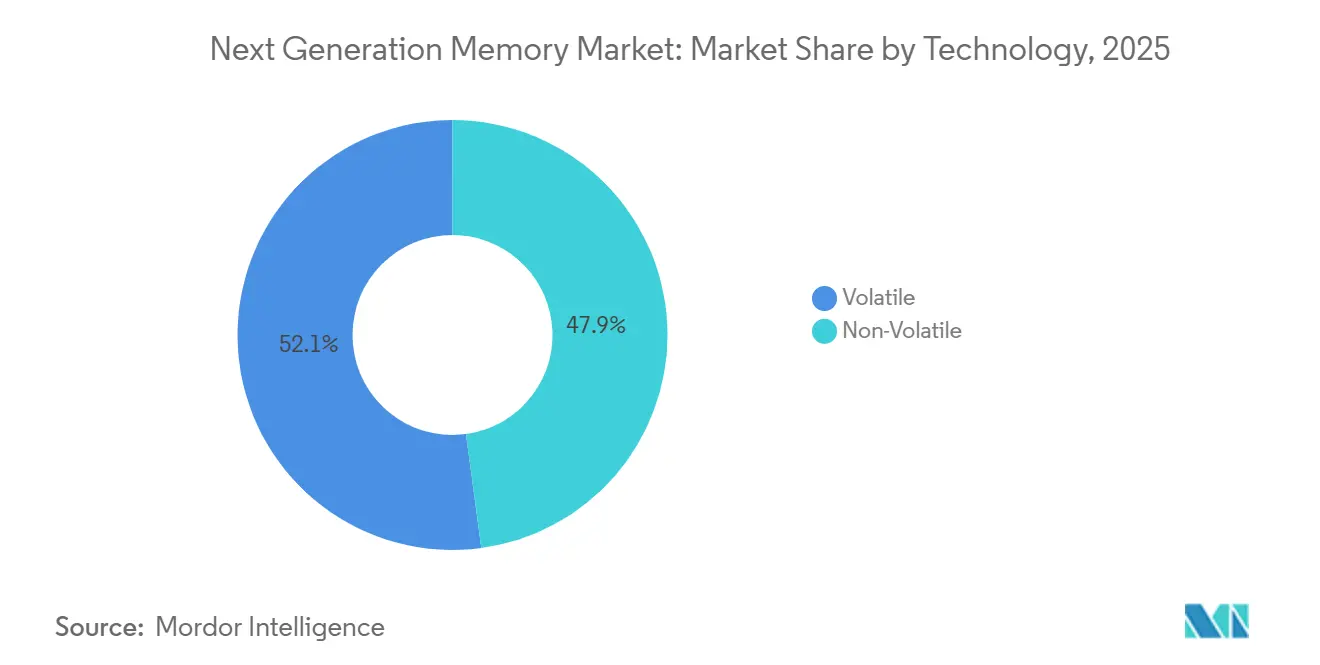
By Technology: Volatile Memory Dominates as Non-Volatile Gains Traction
Volatile secured 52.14% of the next generation memory market share in 2025, reflecting its role as the preferred stack for AI accelerators. The next-generation memory market size for volatile technologies stays elevated as Samsung prepares a 24-layer HBM4 prototype with 1.5 TB/s bandwidth. Spin-Transfer-Torque MRAM, however, is on track for a 23.03% CAGR through 2031 as automotive and industrial buyers prioritize instant-on and radiation-tolerant features.
Non-volatile alternatives such as phase-change memory, toggle MRAM, and resistive RAM collectively accounted for roughly 12% in 2025, with embedded ReRAM moving into payment cards and biometric modules. Ferroelectric RAM remains essential in ultra-low-power industrial sensors, while NanoRAM is advancing in space-grade systems. Discontinuation of Intel Optane in 2024 created a vacuum that STT-MRAM suppliers are exploiting to capture enterprise storage slots.[3]Intel Corporation, “Intel Optane Persistent Memory Overview,” intel.com


By Memory Interface: CXL Emerges as the Fastest-Growing Protocol
In 2025, DDR and LPDDR interfaces commanded a dominant 46.51% share of the revenue, leveraging their backward compatibility and widespread controller support. These interfaces have become a cornerstone in the memory market due to their ability to seamlessly integrate with existing systems and their compatibility with a broad range of controllers. The market for next-generation memory, linked to Compute Express Link, is set to surge at a robust 22.16% CAGR, driven by CXL 3.0's capability to facilitate coherent sharing among 4,096 devices. This growth highlights the increasing demand for advanced memory solutions that can support high-performance computing and data-intensive applications.
While PCIe and NVMe accounted for roughly a third of the revenues, the landscape is shifting as new technologies emerge. Hyperscale buyers are increasingly turning to rack-scale memory fabrics to optimize capacity usage and reduce inefficiencies caused by stranded memory. With Intel's Xeon 6 and AMD's EPYC Genoa integrating native CXL 2.0 controllers, the ecosystem is poised for maturity by 2026, ensuring a more robust and scalable infrastructure for future applications. Although proprietary automotive serial links maintain a specialized foothold, their market share is dwindling as JEDEC moves to standardize CXL extensions for vehicles. This standardization is expected to drive innovation and adoption in the automotive sector, further transforming the competitive dynamics of the memory market.
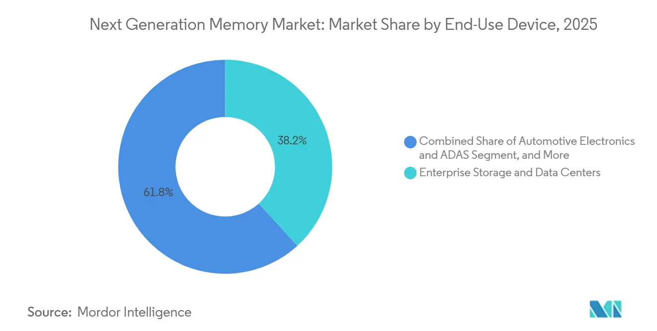
By End-Use Device: Automotive ADAS Outpaces Enterprise Growth
In 2025, HBM3E-rich AI racks propelled enterprise storage and data centers to account for a significant 38.23% of total revenue, highlighting their critical role in the market. These AI racks, equipped with advanced memory technologies, are driving efficiency and performance in enterprise storage solutions. As Level 4 rollouts gain momentum, automotive electronics and ADAS are poised for a robust 23.86% CAGR, showcasing the growing adoption of advanced driver-assistance systems and autonomous vehicle technologies. The consumer electronics segment, buoyed by LPDDR5X driving on-device AI workloads, saw the next-generation memory market capture nearly 27% in 2025, underlining the increasing demand for high-performance memory solutions in consumer devices.
Industrial IoT, harnessing ferroelectric RAM for energy-harvesting condition-monitoring nodes, secured a share of roughly 9%, reflecting its importance in enabling efficient and sustainable industrial operations. While aerospace and defense, with a share of just under 4%, opt for premium-priced radiation-hardened memory, these sectors continue to prioritize reliability and durability in extreme conditions. Healthcare, though a smaller player in the market, benefits from secure ReRAM in portable diagnostics, ensuring patient record protection in line with HIPAA guidelines. This steady growth in healthcare highlights the critical role of secure and reliable memory solutions in advancing medical technologies and safeguarding sensitive patient information.

By Wafer Size: 300 mm Still Dominates While 450 mm Progress Is Slow
In 2025, platforms measuring 300 millimeters held a dominant 67.29% share of the market. The market for next-generation memory, associated with 450 mm substrates, is projected to expand at a rate of 21.44%. This growth hinges on overcoming lithography challenges, which, once addressed, could lead to cost reductions of 25% to 30% at established yields. However, in 2023, both Intel and TSMC halted their 450 mm initiatives. The reason? The capital intensity for each fabrication facility soared beyond USD 15 billion, pushing any potential cost relief to the latter half of the forecast period. Meanwhile, embedded ReRAM suppliers like Crossbar and Weebit Nano are firmly anchored to 300 mm pilot lines, limiting their expansion possibilities.
The delay in transitioning to 450 mm substrates has also impacted the broader semiconductor supply chain. Equipment manufacturers and material suppliers, who had invested heavily in preparation for the shift, are now recalibrating their strategies. This pause has created opportunities for further innovation in 300 mm platforms, as stakeholders focus on optimizing existing technologies to meet growing market demands.
Geography Analysis
In 2025, Asia-Pacific dominated the revenue landscape with a commanding 56.43% share. This significant market leadership was bolstered by South Korea's substantial KRW 26 trillion (USD 19 billion) investment in advanced memory lines, aimed at enhancing production capabilities and technological advancements. Additionally, China's CNY 50 billion (USD 7 billion) expansion at Changxin Memory Technologies further strengthened the region's position by increasing its manufacturing capacity and competitiveness in the global market. Meanwhile, Taiwan and Japan's robust foundry ecosystems played a pivotal role in supporting the region's dominance. These ecosystems streamline the journey from prototype development to mass production, enabling faster time-to-market cycles and fostering innovation across the supply chain.
North America secured approximately 23% of the next-generation memory market in 2025, driven by expansive hyperscale AI deployments that continue to transform industries and create demand for advanced memory solutions. The region also benefited significantly from the USD 39 billion CHIPS Act subsidy, which provided critical funding to bolster domestic semiconductor manufacturing and research capabilities. This strategic investment has positioned North America as a key player in the global memory market, ensuring its competitiveness and resilience. Europe, with a 12% market share, leveraged the EU Chips Act's generous grants of EUR 43 billion (USD 47 billion), which were directed towards embedded memory research and development. Notably, Germany and France collaborated to co-fund pilot lines, aiming to reduce their reliance on imports and establish a more self-sufficient semiconductor ecosystem. These efforts reflect Europe's commitment to strengthening its technological infrastructure and fostering innovation in the memory market.
Though modest in size, the Middle East is making waves with a projected 21.65% CAGR, marking it as the fastest-growing region in the next-generation memory market. This impressive growth is largely attributed to Saudi Arabia and the United Arab Emirates integrating on-device inference into their ambitious smart-city initiatives. These initiatives are designed to enhance urban infrastructure and improve the efficiency of city operations, driving demand for advanced memory technologies. In contrast, South America and Africa lag behind with a combined market share of under 5%. Their growth is stunted by a lack of fabrication infrastructure, which limits their ability to compete on a global scale. However, Brazil's automotive sector presents a promising niche opportunity for automotive-grade MRAM, as the country continues to develop its capabilities in this specialized area. This niche market could serve as a stepping stone for further advancements in the region's memory technology landscape.

Regulatory Landscape
The regulatory environment for next-generation memory is increasingly shaped by industrial-policy instruments tied to supply-chain resilience, alongside efforts to standardize interfaces and modules. In June 2026, the European Commission advanced a proposal commonly referred to as Chips Act 2.0 (COM(2026) 504), reinforcing the EU approach to addressing strategic dependencies in advanced semiconductor segments that include memory and packaging.
On the technical-compliance side, JEDEC activity remains central to ecosystem qualification and interoperability for AI and data center deployments. During 2026, JEDEC published updated module and platform standards such as JESD323B (DDR5 CUDIMM and CQDIMM) and JESD324B (CSODIMM), and introduced JESD328 (SOCAMM2) for AI server and data center module form factors, clarifying electrical, mechanical, and system integration requirements for broader OEM and hyperscaler adoption.
Value Chain Analysis
The value chain covers silicon wafer supply and materials, front-end wafer fabrication (logic base dies and memory arrays on advanced nodes), back-end assembly and test (HBM stacking, TSV, underfill, and thermal solutions), and downstream integration into accelerators, servers, automotive ECUs, and embedded modules. Recent activity points to tighter coupling between device makers and platform owners, with NVIDIA and SK hynix announcing a multiyear co-development partnership for next-generation memory in June 2026 for AI factories.
Additional collaboration also shows up at the interface between memory and compute roadmaps. In March 2026, Samsung and AMD expanded their work around HBM4 supply and next-generation DDR5 alignment, while bottlenecks remain concentrated in advanced packaging and qualified module supply rather than only wafer starts. A July 2026 10-year framework between GlobalWafers and Micron to support US supply chain needs for AI memory also signals upstream moves to secure critical inputs, and JEDEC SOCAMM2 standardization continues to pull ODMs, server OEMs, and memory vendors into structured qualification and production ramps.
Competitive Landscape
In 2025, Samsung Electronics, SK Hynix, and Micron Technology together accounted for an estimated 75% of HBM3E output, indicating a moderate concentration at the top. These industry giants leverage vertical integration to optimize controller firmware and through-silicon-via stacking, enhancing their yields. Meanwhile, startups like Everspin Technologies, Avalanche Technology, Spin Memory, and Weebit Nano are eyeing automotive and industrial markets, collaborating with foundry partners such as GlobalFoundries and SkyWater Technology.
Patent filings surged by 34% in 2025 for spin-orbit torque switching and ferroelectric FET architectures, signaling a shift towards enhancing write endurance. In January 2025, Samsung showcased its commitment to AI accelerators by unveiling a 24-layer HBM4 prototype. Concurrently, STMicroelectronics integrated a 28 nm embedded PCM into automotive microcontrollers, ensuring alignment with ASIL-D safety standards.
Emerging opportunities are evident in CXL memory expanders, an area yet to see a dominant player, and in embedded ReRAM for secure payment card elements. Nantero is eyeing the aerospace sector with its radiation-hardened carbon-nanotube RAM, while Applied Materials is broadening its etch tool portfolio to include magnetic tunnel junctions essential for MRAM.
Next Generation Memory Industry Leaders
Samsung Electronics Co., Ltd.
SK Hynix Inc.
Micron Technology, Inc.
Kioxia Holdings Corporation
Intel Corporation
- *Disclaimer: Major Players sorted in no particular order

Market Opportunities and Future Outlook
A key opportunity is in AI-optimized memory form factors and standards that reduce integration friction for hyperscale and enterprise deployments. JEDEC actions in 2026 define practical whitespace for both new entrants and incumbent expansion in higher-value module categories, including JESD328 (SOCAMM2) for data center memory modules, and continued progress on bandwidth and packaging pathways for HBM4-class designs with standards such as SPHBM4 for organic substrates.
Another opportunity is scaling embedded and edge-grade non-volatile memories through device-level advances and early ecosystem pilots. In June 2026, CEA-Leti reported FeRAM scaled to 22 nm using a 3D capacitor architecture with HZO thin films, placing higher-density ferroelectric memory in focus for edge AI and ultra-low-power workloads where write endurance and energy profiles matter. On the capacity and localization front, CHIPS-linked and regionally anchored buildouts are still reshaping supply availability and customer qualification pathways, with Micron activity tied to its New York fab site and additional investments by memory manufacturers in packaging and HBM capability to serve accelerator and automotive platforms.
Recent Industry Developments
- June 2026: NVIDIA and SK hynix announced a multiyear technology partnership to co-develop next-generation memory for AI factories, aligning memory roadmaps with NVIDIA infrastructure platforms including Vera Rubin. The agreement formalizes co-engineering across performance, power, and packaging requirements, tightening supply-chain coordination for HBM-class products in data center deployments.
- March 2026: Micron shipped samples of a 256GB SOCAMM2 LPDRAM module for data center infrastructure based on a 32Gb LPDDR5X design. The module-level approach supports higher density and serviceability for server architectures adopting standardized AI-focused memory form factors.
- February 2025: Micron announced shipment of samples of 1-gamma (1γ) node-based DDR5 DRAM, targeting higher performance per watt for future compute needs. The node transition strengthens the company's ability to feed next-generation DDR and LPDDR platforms that sit alongside HBM in AI and enterprise systems.


Research Methodology Framework and Report Scope
Market Definition and Coverage
For this study, the next generation memory market is defined as revenue from advanced memory devices used in computing, storage, and embedded systems, where performance, endurance, or power benefits are the main purchase reason versus mainstream legacy memory.
Scope exclusions: Commodity DDR3 and DDR4 DRAM, and conventional planar NAND flash are excluded from this market size.
Segmentation Overview
- By Technology
- Non-Volatile
- Phase-Change Memory (PCM)
- Spin-Transfer MRAM (STT-MRAM)
- Toggle MRAM
- Resistive RAM (ReRAM)
- 3D XPoint / Optane
- Ferroelectric RAM (FeRAM)
- NanoRAM
- Volatile
- High-Bandwidth Memory (HBM)
- Hybrid Memory Cube (HMC)
- Low-Power DDR5 / LPDDR5X
- Non-Volatile
- By Memory Interface
- DDR / LPDDR
- PCIe / NVMe
- SATA
- Others, Memory Interface
- By End-Use Device
- Consumer Electronics
- Enterprise Storage and Data Centers
- Automotive Electronics and ADAS
- Industrial IoT and Manufacturing Automation
- Aerospace and Defense
- Healthcare and Medical Devices
- Others, End-Use Device
- By Wafer Size
- Up to 200 mm
- 300 mm
- 450 mm
- By Geography
- North America
- United States
- Canada
- Mexico
- South America
- Brazil
- Argentina
- Rest of South America
- Europe
- Germany
- United Kingdom
- France
- Italy
- Spain
- Rest of Europe
- Asia Pacific
- China
- Japan
- South Korea
- India
- Australia
- New Zealand
- Rest of Asia-Pacific
- Middle East and Africa
- Middle East
- United Arab Emirates
- Saudi Arabia
- Turkey
- Rest of Middle East
- Africa
- South Africa
- Nigeria
- Kenya
- Rest of Africa
- Middle East
- North America
Data Sources, Market Sizing, and Validation
Desk Research
Desk work was used to set the outer limits of the market and to anchor the model with measurable signals. We referred to public sources such as semiconductor trade statistics published by customs authorities, central bank exchange-rate series, and electronics and semiconductor association briefings, which help us check regional demand direction and pricing pressure.
We also used sources such as company annual reports and investor presentations, official filings, patent databases, and peer-reviewed journals covering memory physics and manufacturing yields, so that technology readiness and adoption claims were kept realistic. In addition, a paid subscription database for company financials and news was used to track capacity announcements and product ramp timelines, and an import and export shipment-level database was selectively reviewed to sense mix shifts in higher-value memory shipments. These desk sources are not exhaustive, and many other public documents were also used for collection, cross-checks, and clarifications.
Primary Interviews and Surveys
Primary discussions were carried out with people involved in memory design, process engineering, sourcing, and system integration, so that desk assumptions could be corrected where pricing and attach rates vary by application. Since this is a global market, inputs were checked across APAC, EMEA, and the Americas to reflect differences in fab footprints, OEM demand pools, and export exposure.
Distribution of primary research fieldwork respondents
| Company type | Respondent position | Region |
|---|---|---|
| Top tier: 36% | CXOs: 17% | APAC: 46% |
| Mid tier: 43% | Functional/Unit leaders: 26% | EMEA: 36% |
| Smaller Players: 21% | Managers: 57% | Americas: 18% |
Market-Sizing & Forecasting
Sizing starts from a top-down build where semiconductor production and trade data is used to reconstruct the addressable memory value pool, which is then filtered to only the next generation technologies based on adoption evidence. To keep totals grounded, we corroborate the result with selective bottom-up approximations such as sampled ASP times estimated shipment volumes for key device families, along with channel checks on program ramps.
Inputs used in the model include (illustrative) wafer starts and capacity additions for relevant nodes, estimated bit shipment growth tied to data center demand, pricing and mix shifts between emerging non-volatile options and high-bandwidth products, regional manufacturing concentration, and typical qualification cycles in automotive and industrial uses. Where bottom-up gaps exist, for example limited disclosure on early ramps, we apply conservative penetration ranges validated by interviews, and then reconcile them back to macro supply signals.
For forecasting, scenario analysis is used so that adoption timing, pricing normalization, and capacity utilization can be flexed without breaking the logic of the model. The forward view is adjusted using expert consensus on ramp pace and substitution behavior, and the final curve is kept consistent with observable constraints like fab readiness and end-market shipment growth.
Data Validation & Update Cycle
Validation is handled through several passes that compare the computed market value with independent signals such as capacity announcements, trade movement trends, and publicly visible pricing direction. When a variance is seen, the assumptions behind ASP, penetration, or regional allocation are revisited, and targeted follow-ups are triggered with interviewees to resolve the mismatch.
Before sign-off, the model and narrative are reviewed by another analyst to confirm the math, logic, and traceability of key inputs. The report is refreshed annually, and interim updates are added when major events occur, such as abrupt pricing swings or large capacity changes. Right before delivery, we do a final sweep so the numbers reflect the latest public information and validated field inputs.
Mordor Intelligence's Next Generation Memory Market Estimate Compared With Other Published Estimates
Published market sizes for next generation memory often differ because the included technology set, the pricing basis, and the assumed ramp timing are not consistent from one publisher to another. In practice, even small differences in what gets counted as next gen memory can shift the number, since newer products tend to carry higher ASPs.
Conventional DDR3 and DDR4 DRAM sit outside Mordor Intelligence's scope here, and that single exclusion usually explains why some broader memory roll-ups land higher even when the growth story sounds similar. Gaps also come from how each estimate treats HBM and other high-bandwidth formats, whether currency conversion uses average-year or spot rates, and how quickly the model moves penetration from pilots into high-volume programs.
Benchmark comparison
| Source | Market Size | Gaps in Research Methodology |
|---|---|---|
| Mordor Intelligence | USD 15.10 B (2025) | |
| Industry Publisher A | USD 10.21 B (2025) | Reported scope is presented as next generation memory, but the public summary does not clearly state which memory families are included or excluded, which can undercount higher-ASP subtypes when coverage is narrower. |
| Global Publisher B | USD 8.25 B (2025) | The disclosed figure is tied to a different base-year setup and limited visible methodology detail, and the lack of clarity on how pricing, mix, and technology inclusion were handled can pull the estimate down versus a wider technology basket. |
Taken together, the spread is mostly explained by scope and the visibility of inputs rather than by a disagreement on long-term demand drivers. Our sizing keeps the market tied to measurable supply and adoption signals, and it stays repeatable because the same inclusion rules and currency treatment can be checked year after year.


Key Questions Answered in the Report
How fast is demand for HBM growing relative to other technologies within the next generation memory market?
Hyperscaler adoption of 12-layer and 16-layer HBM3E stacks is lifting HBM revenue at a pace that adds roughly 6.2 percentage points to overall CAGR, making it the fastest-scaling technology tier through 2028.
Which end-use segment will see the quickest revenue expansion?
Automotive electronics and ADAS are projected to post a 23.86% CAGR between 2026 and 2031 thanks to Level 4 instant-on safety requirements.
What role does Compute Express Link play in future server architectures?
CXL 3.0 enables coherent sharing across more than 4,000 devices, allowing operators to pool memory at rack scale and cutting stranded DRAM capacity across server fleets.
Why is the transition to 450 mm wafers important for the next generation memory market?
Moving to 450 mm substrates could cut per-bit costs by up to 30%, yet lithography roadblocks have postponed volume production beyond 2028, restraining ReRAM cost competitiveness.
Page last updated on:


