Market Overview
| Study Period | 2020 - 2031 |
|---|---|
| Market Size (2026) | USD 33.12 Billion |
| Market Size (2031) | USD 45.54 Billion |
| Growth Rate (2026 - 2031) | 6.58 % |
| Fastest Growing Market | Asia Pacific |
| Largest Market | Asia Pacific |
| Market Concentration | Medium |
Major Players *Disclaimer: Major Players sorted in no particular order Image © Mordor Intelligence. Reuse requires attribution under CC BY 4.0. | |
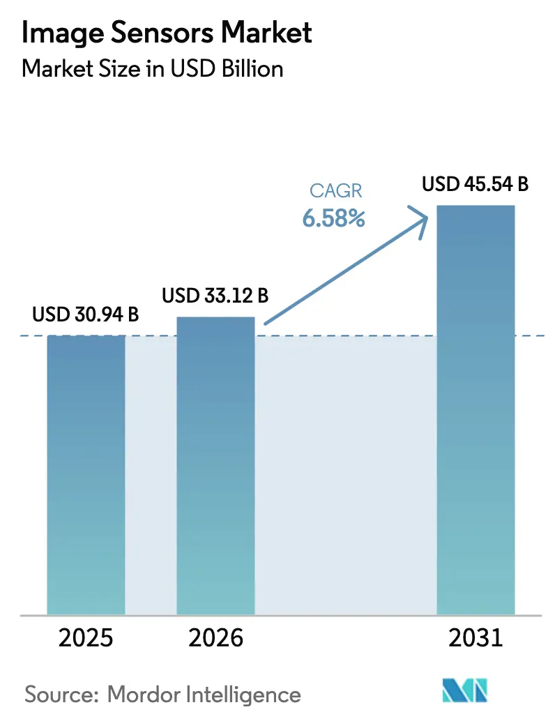
Image Sensors Market Analysis by Mordor Intelligence
The image sensors market size is expected to increase from USD 30.94 billion in 2025 to USD 33.12 billion in 2026 and reach USD 45.54 billion by 2031, growing at a CAGR of 6.58% over 2026-2031. A decade ago, the sector relied on smartphones for almost all volume gains, yet its 2026 profile shows a balanced blend of automotive safety, edge-AI vision, precision agriculture, and industrial quality-control demand. Automotive original-equipment manufacturers (OEMs) are doubling camera counts per vehicle, edge devices are pushing inference to the curb side, and short-wave infrared (SWIR) technology is enabling moisture and contamination detection in food, pharma, and semiconductors. At the same time, foundry constraints on 300 mm complementary-metal-oxide-semiconductor (CMOS) wafers are pushing average selling prices upward, protecting margins even as smartphone unit shipments plateau. Sony, Samsung, and OmniVision defend share through stacked backside-illuminated (BSI) architectures and AI coprocessors, while Chinese challengers such as GalaxyCore and SmartSens battle for mid-tier surveillance and rear-view markets.
Key Report Takeaways
- By processing technology, backside-illuminated architectures captured 44.68% of 2025 revenue, while stacked BSI variants are advancing at 7.34% through 2031.
- By shutter type, rolling-shutter sensors accounted for 76.72% of 2025 shipments; global-shutter designs are growing at 7.51% as Level 3 and Level 4 automated-driving programs scale.
- By spectrum, visible RGB devices held 68.19% share in 2025; SWIR sensors are advancing at 7.59% on the back of precision agriculture and industrial quality-control deployments.
- By end-user industry, consumer electronics held 42.29% of revenue in 2025, but automotive applications are growing at 7.39% as safety mandates and higher driver-monitoring penetration expand camera counts per vehicle.
- By geography, Asia-Pacific led with 44.21% of revenue in 2025, and the region is projected to expand at a 7.65% CAGR through 2031.
Note: Market size and forecast figures in this report are generated using Mordor Intelligence’s proprietary estimation framework, updated with the latest available data and insights as of January 2026.
Market Trends and Insights
Drivers Impact Analysis of Image Sensors Market*
| Driver | (~) % Impact on CAGR Forecast | Geographic Relevance | Impact Timeline |
|---|---|---|---|
| Smartphone Multicamera Proliferation Elevating CMOS Demand | +1.20% | Asia-Pacific core, spillover to North America and Europe | Medium term (2-4 years) |
| Automotive-Grade Global-Shutter Sensors Enabling Level-3+ ADAS | +1.40% | Europe and North America lead, Asia-Pacific scaling | Long term (≥ 4 years) |
| Edge-AI Vision Modules Catalysing Smart-City Investments | +0.90% | Asia-Pacific and Middle East, selective European pilots | Medium term (2-4 years) |
| SWIR Sensors Penetrating Precision-Agriculture and Industrial QC | +0.70% | North America and Europe agriculture, Asia-Pacific manufacturing QC | Long term (≥ 4 years) |
| 3D/Event-Based Sensors Powering Next-Gen AR/VR Wearables | +0.60% | North America and Asia-Pacific consumer markets | Long term (≥ 4 years) |
| Government Safety Mandates Driving In-Cabin DMS Cameras | +0.80% | Europe regulatory lead, China commercial-vehicle mandate, North America voluntary | Short term (≤ 2 years) |
| Source: Mordor Intelligence | |||


Smartphone Multicamera Proliferation Elevating CMOS Demand
Global handset vendors shipped 1.2 billion smartphones with three or more rear cameras in 2025, up 26% year-on-year, as mid-tier models adopted ultra-wide and telephoto modules once reserved for flagships.[1]International Data Corporation, “Worldwide Smartphone Tracker,” idc.com Competitive pressure compressed the bill of materials, forcing sensor suppliers to spread R&D across massive volumes while conceding lower average selling prices. Vertically integrated players such as Sony and Samsung, with captive wafer capacity and image-signal-processor (ISP) cores, are positioned to sustain profitability. Computational photography further shifts value from optics to pixels; algorithms like Apple Deep Fusion and Google Night Sight rely on high dynamic range and low read noise, placing a premium on stacked BSI chips with on-chip 14-bit converters that deliver 120 dB dynamic range.
Automotive-Grade Global-Shutter Sensors Enabling Level 3+ ADAS
Rolling-shutter artifacts become unacceptable when vehicles travel above 100 km/h, prompting OEMs to switch to global-shutter CMOS for forward-facing and surround-view cameras. Mercedes-Benz certified Drive Pilot Level 3 in Germany and California in 2024 using eight global-shutter devices. ON Semiconductor’s Hyperlux platform integrates 3 µm pixels with 140 dB dynamic range, preserving detail in high-contrast scenes.[2]ON Semiconductor, “Hyperlux Automotive Sensors,” onsemi.com Euro NCAP’s 2025 test protocols effectively require pedestrian-detection cameras on all models, accelerating global-shutter penetration.[3]Euro NCAP, “2025 Test Protocols,” euroncap.com
Edge-AI Vision Modules Catalysing Smart-City Investments
Municipal agencies deployed 45 million edge-AI cameras in 2025, embedding neural processing alongside image sensors to cut bandwidth by 80% relative to cloud pipelines. Dubai’s metro network installed 12,000 such units, achieving 95% crowd-density accuracy and rapid return on investment.[4]Dubai Roads and Transport Authority, “Smart Mobility Initiatives,” rta.ae Hardware requirements are shifting toward sub-2 W modules with low-latency rolling shutters, stimulating demand for high-sensitivity 8 MP sensors paired with Qualcomm and NVIDIA edge chipsets.
SWIR Sensors Penetrating Precision Agriculture and Industrial QC
Indium-gallium-arsenide SWIR sensors unlock non-destructive quality checks by imaging at 1,000-2,500 nm. John Deere integrated SWIR cameras in X9 combines, enabling real-time grain-quality feedback. Taiwan Semiconductor Manufacturing Company (TSMC) reduced die-level defect escape by 40% in 5 nm logic thanks to SWIR wafer inspection. Despite camera prices above USD 5,000, cost-per-insight favours deployment in high-value crops and advanced packaging lines. Silicon-compatible colloidal-quantum-dot research at MIT promises sub-USD 500 modules post-2028.
Restraints Impact Analysis of Image Sensors Market*
| Restraint | (~) % Impact on CAGR Forecast | Geographic Relevance | Impact Timeline |
|---|---|---|---|
| 300 mm CIS Wafer Capacity Bottlenecks Creating Price Volatility | -0.60% | Global, acute in Asia-Pacific foundry hubs | Short term (≤ 2 years) |
| Thermal Noise Limits in Sub-1 µm Pixels Hindering Resolution Race | -0.40% | Global, affects premium smartphone and automotive segments | Medium term (2-4 years) |
| Export Controls on Advanced Imaging Chips Impacting Chinese OEMs | -0.50% | China domestic market, spillover to Southeast Asia | Medium term (2-4 years) |
| High Integration Cost of SWIR Sensors Slowing Consumer Uptake | -0.30% | North America and Europe agriculture, Asia-Pacific industrial | Long term (≥ 4 years) |
| Source: Mordor Intelligence | |||
300 mm CIS Wafer Capacity Bottlenecks Creating Price Volatility
Image sensors consumed 180,000 300 mm wafer starts per month in 2025, yet demand exceeded supply by 8%, inflating automotive-grade sensor prices by 12% in early 2025. Sony allocated JPY 200 billion (USD 1.34 billion) to expand its Kumamoto fab by 40,000 wafers per month, but the additional capacity arrives only in late 2026. Fabless vendors lacking long-term contracts face 16-week lead times and margin pressure.
Thermal Noise Limits in Sub-1 µm Pixels Hindering Resolution Race
Pixel pitches under 1 µm double thermal noise, degrading low-light performance. Samsung’s 0.56 µm ISOCELL HP3 needs 16-to-1 pixel binning for acceptable indoor shots, lowering effective resolution to 12.5 MP. Multi-frame noise reduction compensates partially but adds on-chip memory costs of up to 25%. Automotive ISO 26262 standards demand 40 dB SNR, a bar that sub-1 µm pixels cannot reach without sacrificing frame rate.
*Our forecasts treat driver/restraint impacts as directional, not additive. The impact forecasts reflect baseline growth, mix effects, and variable interactions.
Image Sensors Market Segment Analysis
By Type:
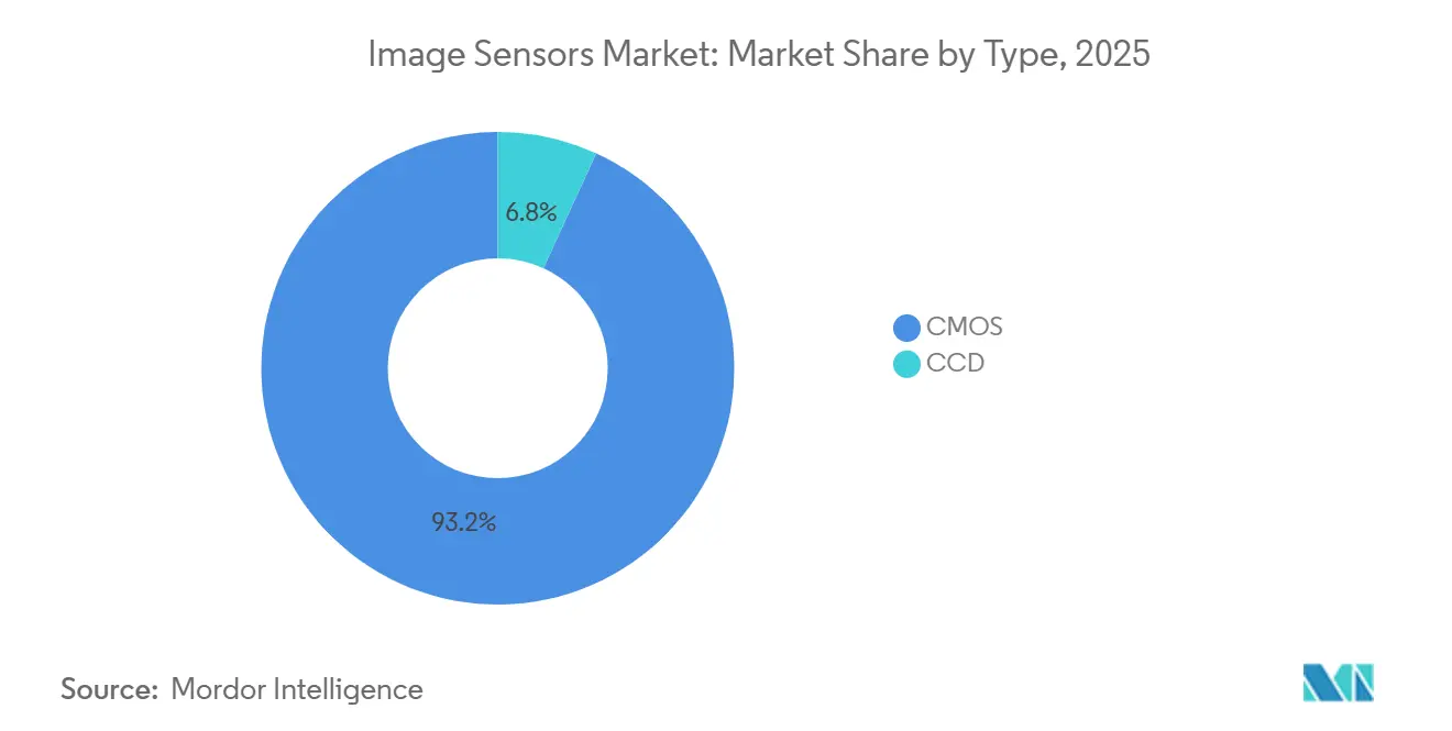
CMOS Dominance Anchors Volume GrowthCMOS devices captured 93.17% of 2025 revenue, a footprint that cements scale economies and drives the image sensors market share advantage over charge-coupled devices (CCD). CMOS integrates readout, analog-to-digital converters, and even neural accelerators on the same die, trimming assembly cost by 30% and power budgets below 500 mW. CCD held 6.83% share in astronomy, pathology, and medical endoscopy, where its sub-electron read noise outweighs slower frame rates. Scientific CMOS, typified by Sony’s IMX661, now delivers 95% quantum efficiency and read noise under 0.3 e-, eroding CCD’s niche. SWIR CMOS, while a small subset today, is expanding 7.11% per year as industrial and agricultural applications migrate from silicon CCD to indium-gallium-arsenide photodiodes.
CCD remains the tool of choice for deep-sky observatories seeking 10-hour integrations with minimal dark current. Medical imaging firms prize CCD uniformity for colour-true tissue differentiation. Yet as the image sensors market size for scientific devices shifts to stacked BSI CMOS with sub-0.5 e- noise, CCD volume is forecast to contract. Niche suppliers will survive on bespoke runs, but mainstream handset, automotive, and vision-system buyers will consolidate around advanced CMOS supply chains.

By Processing Technology:
Stacked Architectures Redefine IntegrationBackside-illuminated technologies owned 44.68% of revenue in 2025. However, stacked BSI is advancing at 7.34% as vendors embed dynamic random-access memory (DRAM) and AI cores under the photodiodes, converting sensors into ultra-low-latency processors. Sony’s IMX989 stacks a 45 nm pixel array atop a 28 nm logic die, cutting image-to-display latency from 50 ms to 5 ms and enabling 14-bit HDR capture. Front-side-illuminated CMOS remains in price-sensitive rear-view cameras, where a 15% bill-of-materials saving still outweighs the 40% sensitivity penalty.
The image sensors market size linked to stacked BSI will keep expanding as heterogeneous integration matures. Canon’s room-temperature surface-activated bonding raises BSI yields by 12 points while meeting automotive defect thresholds. Although through-silicon-via formation adds process steps and 8% cost, OEMs accept the premium for multi-exposure HDR, per-frame AI inference, and lens aberration correction delivered within a 10 mm-square module.
By Shutter Type:
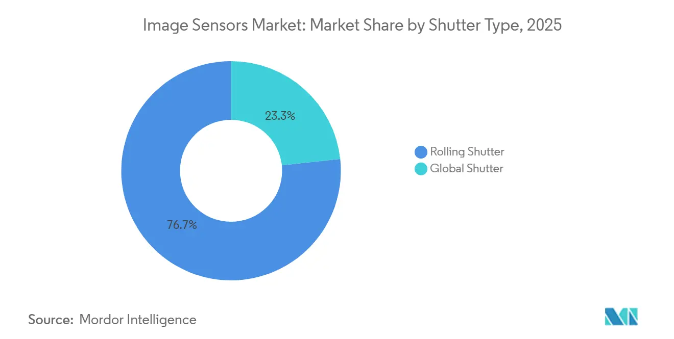
Global Architectures Gain Automotive TractionRolling shutters shipped 76.72% of units in 2025, satisfying smartphones, security cameras, and webcams where scene motion is either moderate or corrected by software. Yet the image sensors market share for global shutters is rising, propelled by Level 3 and Level 4 automated-driving deployments. Automotive suppliers trade a 30% sensitivity loss for artifact-free 8 MP capture at 60 fps. Industrial robotics, drone photogrammetry, and high-speed conveyor inspection similarly depend on global shutters to avoid geometric distortion.
Fill-factor penalties are easing as engineers adopt buried photodiodes and in-pixel correlated double sampling. These advances recover 10 points of quantum efficiency and lift global shutter adoption without exploding die size. Rolling shutters will dominate static-scene and price-critical applications, but regulatory and functional-safety rules guarantee global shutter demand through 2031.
By Spectrum:
SWIR Expands Beyond Visible DominanceVisible RGB sensors accounted for 68.19% of revenue in 2025. Near-infrared (NIR) has already mainstreamed into facial recognition and time-of-flight depth modules. Short-wave infrared is next, with a 7.59% CAGR led by precision agriculture, silicon wafer inspection, and pharmaceutical tablet analysis. High integration cost remains a roadblock, yet MIT’s colloidal-quantum-dot breakthrough hints at sub-USD 500 SWIR modules by 2028.
Silicon-compatible fabrication will unlock mass deployment in food sorting and plastics recycling where moisture discrimination cuts waste. Until then, visible and NIR continue to dominate smartphones and security systems, while X-ray and ultraviolet hold below-5% share in medical and semiconductor lithography due to stringent regulatory and material constraints.
By Resolution:
Megapixel Inflation Meets Computational LimitsThe 4-to-12 MP band held 38.11% share in 2025, balancing detail and data volume for mainstream handsets and 1080p video. Yet sensors above 25 MP are advancing 7.61% annually as computational photography stacks multiple short exposures for 8K video and lossless zoom. Still, diffraction and thermal noise impose limits; a 0.56 µm pixel gathers fewer photons per unit time, forcing heavy pixel binning under low-lux conditions.
Professional shooters and automotive vision teams increasingly emphasize dynamic range and low read noise over headline pixel counts. Canon’s 45 MP EOS R5 Mark II with 15-stop range illustrates this preference. Mobileye and Tier 1s converge on 8 MP for forward-facing cameras, meeting 100-m pedestrian detection while capping bandwidth under 1 GB/s. Ultra-high-resolution chips above 50 MP will stay in medium-format aerial imaging where larger die areas can host 3-5 µm pixels without thermal penalties.
By End-User Industry:
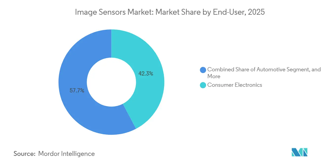
Automotive Outpaces Consumer ElectronicsConsumer electronics delivered 42.29% of 2025 revenue, but its growth is slowing as smartphone replacement cycles lengthen past three years. Automotive, expanding 7.39% through 2031, is the fastest-growing vertical as camera counts ramp from six units in 2024 to a projected 12 units per vehicle by 2030. Industrial robots, bin-picking systems, and edge-AI surveillance collectively form the next growth block.
Healthcare and life sciences adopt IEC 60601-compliant sensors for surgical endoscopy and digital pathology, while aerospace relies on radiation-hardened detectors for satellites. Smart-city and precision-agriculture initiatives tap SWIR and NIR imaging for traffic optimization and drought mitigation. The revenue mix shift is clear: high-value automotive and industrial units now command up to 12% of system cost versus 3% in smartphones.

Geography Analysis
APAC Image Sensors Market
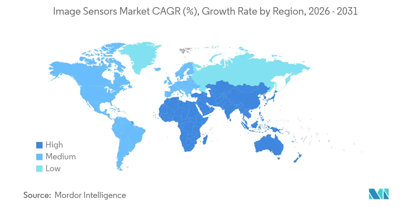
Asia-Pacific contributed 44.21% of 2025 revenue and is projected to grow 7.65% CAGR to 2031. China assembled 68% of smartphones and 52% of security cameras, giving local sensor firms a home-field advantage despite export-control headwinds. Japan’s Sony and Canon retained half of global premium revenue from stacked BSI and scientific CMOS, while South Korea’s Samsung leveraged LPDDR5 memory stacking to break 8K recording barriers.
Europe and North America Image Sensors Market
Europe and North America pooled 38% of revenue. The European Union’s General Safety Regulation, effective July 2024, mandates automated emergency braking and lane-keeping assist, lifting camera content. STMicroelectronics and ams OSRAM supply AEC-Q100 sensors that operate from -40 °C to +105 °C, anchoring a defensible European franchise. North American momentum splits between Tesla’s 12-camera Full Self-Driving suite and Amazon’s 50,000 vision-guided robots.
MEA and South America Image Sensors Market
The Middle East, Africa, and South America captured the remaining 18%. Dubai, Riyadh, and Doha rolled out smart-city edge vision, while Saudi Arabia’s NEOM ordered 100,000 AI cameras worth USD 300 million. South Africa’s mines deployed thermal imagers on autonomous haul trucks, and Brazil’s agribusiness tested SWIR-enabled irrigation. Infrastructure constraints and foreign-exchange volatility temper accelerated uptake, but project-based spikes create localized demand peaks.

Regulatory Landscape
Policy and standards activity around AI-enabled cameras and advanced semiconductors is tightening performance, security, and trade-compliance requirements that filter into image sensor selection and supply chains. In the European Union, the AI Act framework (in force since 2024, with phased applicability) is shaping how providers and operators manage risk for AI systems embedded in vision endpoints, while ETSI EN 303 645 revisions highlighted in 2026 add a cybersecurity-oriented compliance reference point for connected consumer and IoT devices that increasingly incorporate cameras.
In the United States, trade and export-control administration adds direct cost and licensing friction for certain high-end semiconductor and imaging subsystems. A January 2026 Section 232 proclamation introduced 25% ad valorem duties for specified semiconductor categories and derivative products, and BIS continues enforcement actions for controlled thermal imaging technologies under the Export Administration Regulations (EAR). This reinforces the need for classification, licensing, and re-export compliance for sensor modules sold into defense-adjacent and cross-border channels.
Competitive Landscape
Sony, Samsung, and OmniVision controlled roughly 65% of 2025 revenue, giving the image sensors market a moderately concentrated profile. Sony holds a 40% lead by mixing stacked BSI and proprietary event-based cores for AR headsets. Samsung integrates LPDDR5 DRAM beneath sensors, enabling 8K 60 fps video on Exynos phones without throttling. OmniVision covers the cost-sensitive automotive rear-view niche via 1 µm pixels and AEC-Q100 qualification.
Chinese challengers GalaxyCore and SmartSens seized 15% combined share in 2025 through security-camera and rear-view design wins, yet they face advanced lithography restrictions that prevent sub-0.7 µm mass production. Specialty suppliers target white-space opportunities: Prophesee raised USD 54 million to commercialize event-driven vision that reduces data by 90%; Teledyne FLIR dominates SWIR and long-wave infrared industrial inspection. Canon filed 127 patents on dual-gain architectures supporting 140 dB dynamic range, indicating a shift in competitive focus from megapixels to system-in-package integration.
The strategic battleground now centers on heterogeneous integration. Winning vendors will co-package high-speed DRAM, AI inference cores, and power-management ICs within 10 mm modules, slashing latency and enabling real-time analytics. Foundry access, packaging yield, and IP portfolios will decide share shifts more than raw pixel counts.
Image Sensors Industry Leaders
Sony Group Corp.
Samsung Electronics Co., Ltd.
OmniVision Technologies, Inc.
STMicroelectronics N.V.
ON Semiconductor Corporation
- *Disclaimer: Major Players sorted in no particular order
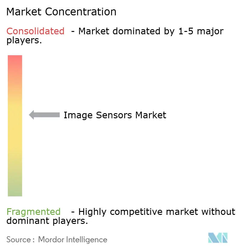
Image Sensors Market Companies Covered in this Report
- Sony Group Corp.
- Samsung Electronics Co., Ltd.
- OmniVision Technologies, Inc.
- STMicroelectronics N.V.
- ON Semiconductor Corporation
- Canon Inc.
- Panasonic Holdings Corporation
- Teledyne DALSA Inc.
- ams OSRAM AG
- SK hynix Inc.
- GalaxyCore Inc.
- Hamamatsu Photonics K.K.
- SmartSens Technology
- PixArt Imaging Inc.
- Himax Technologies, Inc.
- Tower Semiconductor Ltd.
- Teledyne e2v
- Gpixel Inc.
- Forza Silicon Corp.
- Toshiba Electronic Devices and Storage Corp.
- Pyxalis S.A.

Market Opportunities and Future Outlook
Two whitespace areas are expanding as demand shifts from commodity pixel scaling toward application-specific capability: (1) stacked BSI sensors that co-package logic and DRAM to push HDR, low-latency capture, and on-sensor pre-processing for edge-AI cameras used in smart-city deployments and industrial quality control, and (2) automotive-grade global-shutter and high-dynamic-range sensors that align with functional-safety expectations for higher-speed ADAS perception. The market is already showing pull in this integration direction, with municipal deployments of edge-AI cameras in 2025 alongside automotive programs increasing camera counts per vehicle, which rewards suppliers that can deliver low-power modules with predictable latency and robust performance in high-contrast scenes.
Supply-chain and manufacturing partnerships also create room for vendors that can secure advanced process access and packaging yields amid 300 mm CIS constraints. Sony Semiconductor Solutions and TSMC signing a July 2026 non-binding MOU around a next-generation image sensor joint venture in Kumamoto is a concrete example of the industry aligning design leadership with foundry process capability to accelerate stacked architectures. On the product side, Sony Semiconductor Solutions moving LYTIA 610 into mass-production shipments in late June 2026, and announcing LYTIA L910 with LOFIC-equipped HDR, supports continued commercialization momentum for higher-value sensors that compete on dynamic range, latency, and system-level outcomes rather than headline megapixels alone.
Recent Industry Developments in Image Sensors Market
- June 2026: Sony Semiconductor Solutions announced the LYTIA 610 1/2-type 64-effective-megapixel CMOS image sensor for mobile applications, featuring its RB2x2 On-Chip Lens pixel structure, with mass-production shipments starting at the end of June 2026. The release supports the ongoing shift toward stacked and optically optimized architectures that improve sensitivity and autofocus performance without relying solely on smaller pixels.
- January 2025: ams OSRAM received European Commission approval for an EUR 227 million investment grant supporting expansion of semiconductor manufacturing in Austria, as part of a total program reaching EUR 567 million by 2030 for next-generation optoelectronic sensors. The funding strengthens regional supply capacity for sensing components used across camera-adjacent modules and industrial and automotive optical systems.
- November 2024: Hamamatsu Photonics acquired BAE Systems Imaging Solutions and rebranded it as Fairchild Imaging to expand its opto-semiconductor presence and deepen its North American footprint. The deal expands Hamamatsu's positioning in specialized imaging devices used in defense, industrial, and scientific applications that sit adjacent to the broader image sensor market.


Image Sensors Market Report Scope and Research Methodology
Market Definition and Coverage
For this study, the image sensors market covers revenue earned from selling solid-state imaging sensors used to capture light and convert it into digital signals across devices and systems, and it is measured at the point of sensor shipment and use.
Scope exclusions: We exclude downstream camera modules, lenses, image signal processors sold as standalone chips, and services such as integration, calibration, and maintenance.
Segments Covered in This Report
- By Type
- CMOS
- CCD
- By Processing Technology
- Front-Side Illuminated (FSI)
- Back-Side Illuminated (BSI)
- Stacked BSI
- By Shutter Type
- Rolling Shutter
- Global Shutter
- By Spectrum
- Visible (RGB)
- Near-Infrared (NIR)
- Short-Wave Infrared (SWIR)
- X-ray / Ultraviolet
- By Resolution
- Less than 1 MP
- 1 - 3 MP
- 4 - 12 MP
- 13 - 24 MP
- More than Equal to 25 MP
- By End-User Industry
- Consumer Electronics
- Automotive and Transportation
- Industrial Automation and Robotics
- Security and Surveillance
- Healthcare and Life Sciences
- Aerospace and Defense
- Smart City, Agriculture, Marine
- By Geography
- North America
- United States
- Canada
- Mexico
- Europe
- United Kingdom
- Germany
- France
- Italy
- Rest of Europe
- Asia-Pacific
- China
- Japan
- India
- South Korea
- Rest of Asia-Pacific
- Middle East
- Israel
- Saudi Arabia
- United Arab Emirates
- Turkey
- Rest of Middle East
- Africa
- South Africa
- Egypt
- Rest of Africa
- South America
- Brazil
- Argentina
- Rest of South America
- North America
Data Sources, Market Sizing, and Validation
Desk Research
Desk work was used to set the market boundaries and build the first data scaffolding for supply, pricing direction, and end-market demand. We relied on public sources such as government trade statistics and customs portals, central bank and official inflation series, standards bodies and technical publications, patent databases, and peer-reviewed journals that track imaging technology progress.
To convert that foundation into a workable sizing model, we also reviewed annual reports and investor presentations, product briefs, association websites, and reputable press coverage that discusses camera adoption in phones, autos, factories, and security systems. Paid subscriptions focused on company financials and news intelligence, plus patent and shipment-level import and export views where relevant, were used to clarify company exposure and shipment flows. The above list is not exhaustive, and many other sources were used to collect data, validate assumptions, and resolve research questions.
Primary Interviews and Surveys
Primary discussions were run with a mix of sensor suppliers, device makers, channel participants, and industry experts who track imaging demand and pricing. We used these conversations to confirm the scope cut between sensors and adjacent components, and to test assumptions on resolution mix, CMOS versus CCD demand, and average selling price (ASP) movement across major use cases and regions.
Distribution of primary research fieldwork respondents
| Company type | Respondent position | Region |
|---|---|---|
| Top tier: 38% | CXOs: 19% | APAC: 41% |
| Mid tier: 41% | Functional/Unit leaders: 40% | EMEA: 32% |
| Smaller Players: 21% | Managers: 41% | Americas: 27% |
Market-Sizing & Forecasting
Sizing starts with a top-down build where device production and trade signals are translated into a demand pool for sensors, and then split by the main technology and use patterns seen in imaging. Once that structure is in place, selective bottom-up checks are used to keep totals realistic, such as rolling up a sample of supplier revenues, validating major application volumes, and applying ASP-by-spec assumptions where interview feedback is consistent.
Key inputs in the model include smartphone and consumer device output trends, vehicle camera penetration (especially ADAS and in-cabin), industrial and security camera deployments, and the product mix shifts by resolution tier, shutter type, and spectrum needs (for example, visible versus NIR and SWIR). Because prices in sensors can move quickly with node changes, wafer supply tightness, and spec upgrades, ASP logic is treated as its own track that is updated by resolution and processing technology rather than using one flat price. For forecasting, we use scenario analysis supported by simple multivariate relationships between end-market production, camera penetration, and expected ASP steps, and then align the final curve to what primary experts consider a realistic adoption path.
Where bottom-up data is patchy, gaps are handled through ratio-based allocation using observable indicators, such as the regional device build mix and application share confirmed in interviews, which are then reviewed so outliers do not distort totals.
Data Validation & Update Cycle
Validation is done in layers so the final number is not driven by one noisy signal. We cross-check the model against independent markers such as reported revenue exposure, shipment direction from trade statistics, and the implied sensor content per device, and then any variance that breaks normal price or volume behavior is reviewed before sign-off.
Before publishing, the work is reviewed across analysts to confirm scope consistency, unit conversions, and currency handling, followed by targeted re-contacts when a driver looks unstable (for example, a sudden ASP drop or a sharp shift in automotive camera content). Reports are refreshed annually, and interim updates are made when material events occur, such as major supply constraints or demand resets. Right before delivery, an analyst runs a fresh pass so clients receive the latest updated view.
Mordor Intelligence's Image Sensors Market Estimate Compared With Other Published Estimates
Published market sizes for image sensors often do not match because teams make different choices on what gets counted as a sensor sale and how they treat fast-moving pricing. The year used, currency timing, and how quickly assumptions are refreshed also matter more here than in many steadier component markets.
A common split is whether adjacent items are included, like camera modules, lenses, or bundled imaging subsystems, which can lift totals even when the sensor volumes are the same. The second big driver is ASP modeling, where some estimates apply a broad blended price, while others separate pricing by resolution, processing approach, and specialty spectrum needs, and then adjust for mix changes. The spread can also widen when one estimate is anchored to an older exchange rate set or a prior-year price curve, which is why the monthly currency timing and refresh checks used in the latest update cycle are a key reason the 2026 view differs in Mordor Intelligence.
Benchmark comparison
| Source | Market Size | Gaps in Research Methodology |
|---|---|---|
| Mordor Intelligence | USD 33.12 B (2026) | |
| Global Consultancy A | USD 36.94 B (2026) | The estimate appears to use a broader image-sensing scope that can capture more bundled imaging content, and it also implies a higher blended ASP track that is less constrained by resolution and processing mix steps. |
| Industry Publisher B | USD 25.07 B (2024) | The figure is anchored to an earlier base year and can understate later price and mix upgrades, and the currency timing and update cadence between 2024 and 2026 can widen the gap when exchange rates and component pricing move. |
Taken together, the comparison shows that scope boundaries and ASP mechanics are usually the main swing factors, followed by base year and currency timing choices. By keeping the sensor-only boundary clear and updating price and mix inputs in step with real adoption signals, we can provide a market size that is easier to trace back to repeatable drivers.


Key Questions Answered in the Report
What is the projected revenue for the image sensors market in 2031?
The image sensors market is forecast to reach USD 45.54 billion by 2031.
Which region is expected to grow the fastest through 2031?
Asia-Pacific, expanding at a 7.65% CAGR, driven by consumer-electronics assembly in China and automotive demand in Japan and South Korea.
Why are global-shutter sensors important for automated driving?
They eliminate motion artifacts at highway speeds, meeting functional-safety requirements for Level 3 and Level 4 driver-assistance systems.
What is constraining sub-1 µm pixel performance?
Thermal noise doubles as pixel area shrinks, lowering signal-to-noise ratios and forcing heavy pixel binning in low light.
How will stacked BSI technology influence future camera modules?
By embedding AI cores and DRAM under the photodiodes, stacked BSI cuts latency from 50 ms to 5 ms and enables real-time HDR and depth processing.
Which vertical is set to outpace consumer electronics in growth?
Automotive, as safety mandates and rising camera counts push a 7.39% CAGR through 2031.
Page last updated on: