
High Bandwidth Memory Market Size and Share
High Bandwidth Memory Market Analysis by Mordor Intelligence
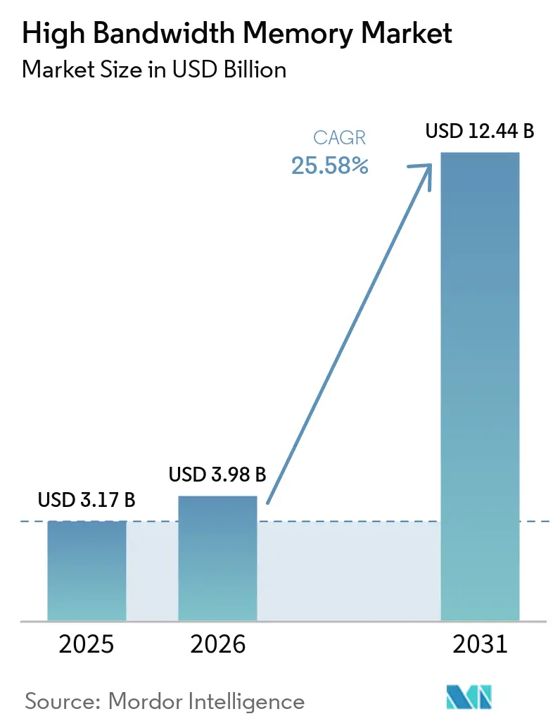
The high bandwidth memory market size is expected to increase from USD 3.98 billion in 2026 to USD 5 billion in 2027 and reach USD 15.99 billion by 2032, growing at a CAGR of 26.18% over 2027-2032.
Cloud expansion links HBM demand to AI training platforms and the memory content built into each computing system. Larger stacks create another route to increase memory content within an accelerator design. Manufacturers can gain from these configurations, but stack defects and limited assembly capacity can delay finished computing hardware. US export licensing and Chinese government restrictions on licensed H200 sales in China, beginning in February 2026, complicate accelerator access. Added memory content reaches buyers only when stack output and assembly slots align, with covered sales also requiring permitted customer access.
Key Report Takeaways
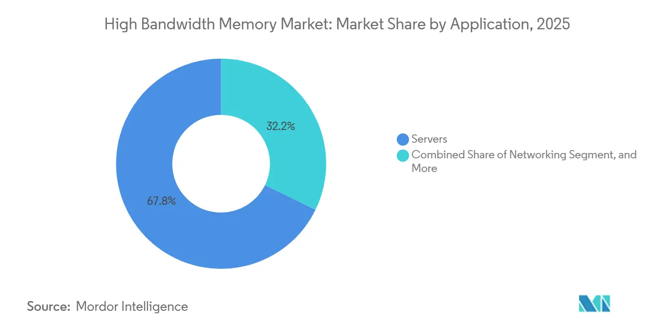
- By application, servers led with a 68.13% high bandwidth memory market share in 2026, while automotive and transportation is forecast to grow fastest at a 27.4% CAGR over 2027-2032.
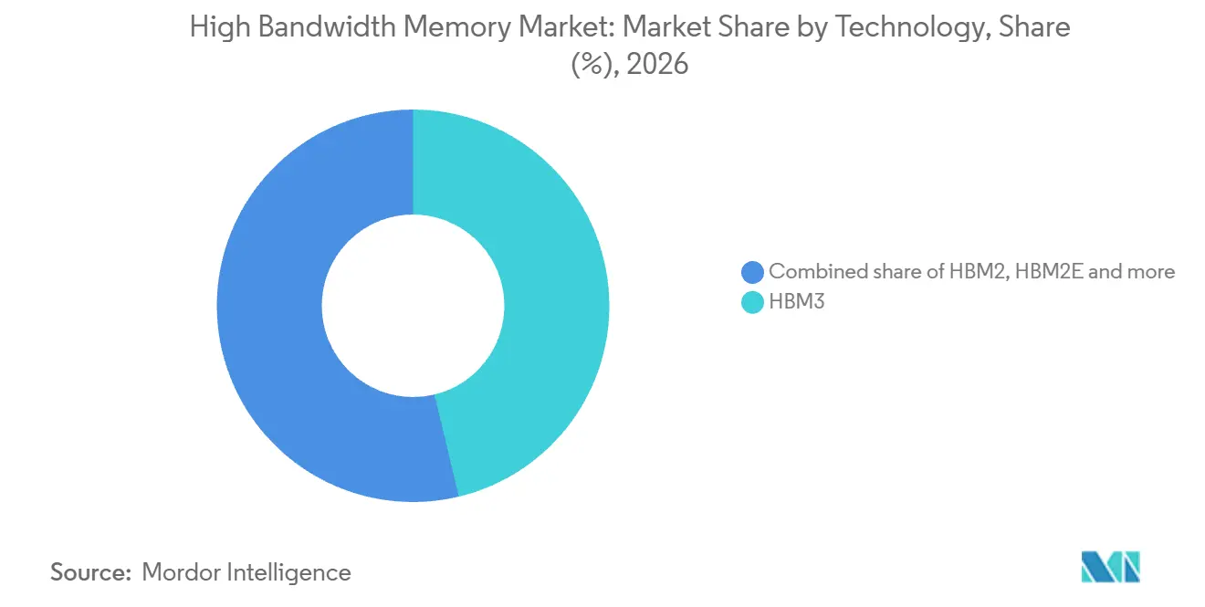
- Within technology, HBM3 accounted for a 46.25% share of the high bandwidth memory market size in 2026, and HBM3E is projected to be the fastest-growing segment with a 27% CAGR over 2027-2032.
- By memory capacity per stack, 16 GB stacks led with a 38.59% share in 2026, while stacks of 32 GB and above are forecast to grow fastest at a 27.2% CAGR over 2027-2032.
- Across processor interfaces, GPUs held the largest share at 63.83% in 2026, with AI accelerators and ASICs projected to post the fastest growth at a 26.6% CAGR over 2027-2032.
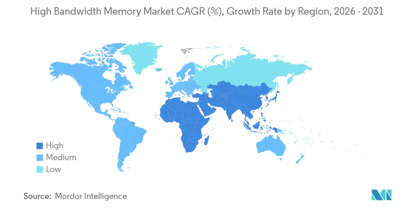
- Geographically, Asia-Pacific led with a 41.31% share in 2026 and is forecast to be the fastest-growing region with a 26.9% CAGR over 2027-2032.
Note: Market numbers in this report are based on Mordor Intelligence's proprietary estimation framework, which combines nine months of actuals with Q4 projections for base year 2026.
Market Trends and Insights
Drivers Impact Analysis of High Bandwidth Memory Market*
| Driver | (~) % Impact on CAGR Forecast | Geographic Relevance | Impact Timeline |
|---|---|---|---|
| AI-Server Proliferation and GPU Attach Rates | +18% | United States AI-compute centers | Short term (≤ 2 years) |
| Data-Center Shift to DDR5 and 2.5-D Packaging | +7% | South Korea packaging centers | Medium term (2-4 years) |
| Edge-AI Inference in Automotive ADAS | +3% | United States automotive development | Medium term (2-4 years) |
| Hyperscaler Preference for Silicon Interposer Stacks | +4% | United States cloud-computing locations | Medium term (2-4 years) |
| Localized Memory Production Subsidies (KR, US, JP) | +2% | Japan advanced-memory manufacturing locations | Long term (≥ 4 years) |
| Photonics-Ready HBM Road-Maps | +1% | United States, South Korea and Singapore | Long term (≥ 4 years) |
| Source: Mordor Intelligence | |||
AI-Server Proliferation and GPU Attach Rates
Cloud expansion increases the HBM opportunity through both the number of accelerators deployed and the memory content of each system. In less than a year through March 2026, Microsoft deployed hundreds of thousands of liquid-cooled Grace Blackwell GPUs across its global data-center footprint.[1] The United States is one operating location, with Microsoft reporting advanced AI supercomputers in its Greater Atlanta Metro footprint in December 2025. NVIDIA specifies 72 Blackwell GPUs and 13.4 TB of HBM3E per GB200 NVL72 system. Rack configuration therefore determines how GPU deployment translates into memory requirements, so accelerator counts alone cannot specify HBM supply needs.
Data-Center Shift to DDR5 and 2.5-D Packaging
Data-center accelerators and host processors create complementary memory requirements within the same commercial computing service. Oracle's OCI BM.GPU.MI300X.8 bare-metal instance combines 8 AMD Instinct MI300X GPUs, 1.5 TB of aggregate GPU HBM3 and 2 TB of DDR5 system memory. Oracle operates the cloud service, while AMD supplies the accelerators. TechInsights' April 2025 analysis of NVIDIA's GB100 GPU identified 8 HBM packages co-packaged with TSMC silicon and described CoWoS-L as a commercial packaging technology. Co-packaging places HBM supply within the accelerator's assembly requirements, connecting memory demand to package integration as well as cloud-instance configuration.
Edge-AI Inference in Automotive ADAS
Off-vehicle training for driving models creates an HBM requirement in automotive development infrastructure. In Q2 2025, Tesla added 16,000 H200 GPUs to Cortex at Gigafactory Texas, bringing its compute capacity to 67,000 H100 equivalents. NVIDIA specifies the H200 with 141 GB of HBM3E memory at 4.8 TB/s. Tesla operated Cortex as off-vehicle training infrastructure for its supervised FSD system. Because each added H200 carries 141 GB of HBM3E, the expansion attached a large block of stacked memory to one automaker's model-development capacity.
Hyperscaler Preference for Silicon Interposer Stacks
A hyperscaler's own accelerator platform can establish an HBM requirement before cloud customers select the computing service. Google Cloud makes TPU7x Ironwood available for AI training and inference, with 192 GiB of HBM per chip. Google designs and operates the TPU platform and offers access through its cloud service. TechSearch International's October 2025 presentation identified TSMC's CoWoS-R package for AWS Trainium2 training and inference. The supply opportunity therefore begins with the operator's hardware platform, where memory content and package integration must be designed together.
Restraints Impact Analysis of High Bandwidth Memory Market*
| Restraint | (~) % Impact on CAGR Forecast | Geographic Relevance | Impact Timeline |
|---|---|---|---|
| TSV Yield Challenges Above 12-Layer Stacks | -3.5% | South Korea manufacturing centers | Medium term (2-4 years) |
| Limited CoWoS/SoIC Advanced-Packaging Capacity | -3% | Taiwan advanced-packaging centers | Short term (≤ 2 years) |
| Thermal Throttling in HBM Devices | -1.5% | South Korea production centers | Medium term (2-4 years) |
| Geo-Political Export Controls on AI Accelerators | -1% | United States and China | Short term (≤ 2 years) |
| Source: Mordor Intelligence | |||
TSV Yield Challenges Above 12-Layer Stacks
Manufacturing yield can constrain high-capacity HBM before additional memory reaches accelerator builders. In August 2026, Semiconductor Engineering, citing industry insiders, reported that more TSVs, thinner dies, underfill voids and process variation could impair yield and DRAM supply in taller stacks.[2] The article said any one of these defects can turn the entire stack of dies into very expensive scrap, and it cited SK hynix's work on 16-high HBM as exposing further critical manufacturing factors. This makes usable output, rather than the number of dies processed, the commercially relevant measure for suppliers expanding stack height. For accelerator builders, a capacity upgrade therefore depends on reliable stack production as well as the memory design. The constraint puts the cost of discarded assemblies directly against the value of adding more memory per stack.
Limited CoWoS/SoIC Advanced-Packaging Capacity
Packaging availability sets a separate ceiling on how quickly accelerator vendors can turn HBM stacks into finished computing systems. In October 2025, TSMC said CoWoS capacity was short of demand and it was working to narrow that gap. On October 15, 2026, the company described a small back-end capacity shortage while discussing interposer cooperation with GlobalFoundries. Such an assembly constraint can limit product deliveries even when additional memory stacks become available. TSMC said it wanted to work with GlobalFoundries to provide enough capacity for customer product introductions. The remaining exposure is a delivery delay that additional standalone HBM output cannot by itself remove.
*Our forecasts treat driver/restraint impacts as directional, not additive. The impact forecasts reflect baseline growth, mix effects, and variable interactions.
High Bandwidth Memory Market Segment Analysis
By Application:
Server Scale and Automotive Program PotentialServers accounted for a 68.13% share of the high bandwidth memory market size in 2026. In Q2 2026, SK hynix said high-performance AI-server products led price increases amid sustained demand growth from AI infrastructure investment. The company said that pricing helped it exceed the previous quarter's record performance. SK hynix's statement shows AI-server buyers paying higher prices for high-performance products, so server demand lifts producer results through price as well as through the number of systems built.
Automotive and transportation is the fastest-growing application segment, with a 27.4% CAGR forecast over 2027-2032. Automotive and transportation starts from a much smaller revenue position than servers. Even at the faster rate, the revenue it adds over 2027-2032 stays well below what servers add, so the segment shifts the application mix only gradually.

By Technology:
HBM3 Installations and HBM3E Product MixHBM3 represented a 46.25% high bandwidth memory market share in 2026, making it the largest technology segment. Petrobras reported Harpia was operating in October 2025. The Brazilian system appeared on TOP500's June 2026 list with NVIDIA H100 SXM5 GPUs that use HBM3. Harpia began operating in October 2025 on H100 GPUs that use HBM3, so a newly commissioned system in 2025 still relied on HBM3, which fits the generation's position as the largest technology segment.
HBM3E is the fastest-growing technology segment, with a 27% CAGR forecast over 2027-2032. In Q3 2025, SK hynix said increased sales of high-value 12-high HBM3E products contributed to its record quarterly performance as customer investment in AI infrastructure lifted memory demand. This links expansion to sales of a high-value stack configuration within HBM3E, without requiring a shift to an entirely different memory generation. Growth within HBM3E can involve a richer product mix, giving suppliers a route to higher revenue per stack alongside unit demand.
By Memory Capacity per Stack:
Stack Content and Processor Memory ScaleThe 16 GB stack segment held the largest share, at 38.59% in 2026. In June 2026, TOP500 recorded SSC-24 in South Korea as a computing system operated by Samsung Electronics and supplied by HPE, using NVIDIA H100 SXM5 GPUs. NVIDIA identifies 80 GB of HBM3 across 5 stacks for that GPU configuration. This arrangement connects an individual stack-capacity tier to a substantially larger GPU memory total. Each H100 SXM5 processor requires 5 stacks of 16 GB, so one additional processor represents demand for multiple stacks.
The 32 GB and above segment is the fastest-growing capacity segment, with a 27.2% CAGR forecast over 2027-2032. Micron Technology, Inc. began volume shipments of 36 GB HBM4 12H stacks in Q1 2026, designed for NVIDIA Vera Rubin. A larger stack can raise the memory capacity incorporated into a processor design when the stack count is held constant. For accelerator vendors, that creates an alternative to increasing the number of memory stacks to obtain more capacity. Micron's volume shipments establish a supply route for this tier, with adoption tied to accelerator designs that specify higher-capacity stacks.
By Processor Interface:
GPU Shipments and Custom Cloud AcceleratorsGPUs were the largest processor-interface segment, with a 63.83% share in 2026. Epoch AI estimated that NVIDIA B300 shipments through Q4 2025 incorporated a cumulative 431.7 PB of HBM and 12.01 EB/s of memory bandwidth. A single GPU product line thus carries a substantial memory requirement, supporting the importance of GPU programs as a channel for HBM suppliers. Because those shipments carry bandwidth as well as capacity, GPU programs set demand for stack speed as well as stack count.
AI accelerators and ASICs are the fastest-growing processor-interface segment, with a 26.6% CAGR forecast over 2027-2032. In May 2026, Google reported that customers were using Ironwood at scale for demanding AI training jobs. Google Cloud specifies 7,380 GBps of HBM bandwidth per Ironwood chip, so every chip customers train on carries a defined bandwidth requirement for its memory. Sustained customer training therefore ties HBM demand for this segment to Google's own accelerator deployments.
Geography Analysis
Asia-Pacific High Bandwidth Memory Market
Asia-Pacific accounted for a 41.31% share of the high bandwidth memory market size in 2026 and is the largest and fastest-growing region, with a 26.9% CAGR forecast over 2027-2032. In its Q2 2026 business results, South Korea-based memory producer SK hynix said customer demand for its products exceeded its supply capabilities. The company announced a Yongin fab plan in August 2026 for HBM and next-generation DRAM, targeting its first cleanroom opening in June 2029. In September 2026, Micron said cleanroom preparation at its Singapore HBM advanced-packaging facility was ahead of plan, with initial output expected in early calendar 2027. The planned additions target initial packaging output in early 2027 and new fabrication space in June 2029, so they address supply growth beyond the shortfall SK hynix described in Q2 2026.
In North America, Argonne opened Aurora to users on January 27, 2025, and the system has 64 GB of HBM per Intel Xeon CPU Max processor and 128 GB per Intel GPU Max unit. In Europe, JUPITER was inaugurated in Jülich, Germany, in September 2025, with an Eviden-supplied Booster containing approximately 24,000 HBM-equipped NVIDIA GH200 Grace Hopper Superchips. Spain's MareNostrum 5 has 72 HBM compute nodes, each with 128 GB of HBM. Scientific computing in the United States and Spain creates an HBM application beyond GPUs, adding CPU-equipped systems to the supplier opportunity.
In South America, Brazil's Federal University of Santa Catarina inaugurated VLAB@UFSC in April 2025 for AI research and applications with an NVIDIA DGX H100, whose reference configuration includes HBM3. UFSC offers the DGX H100 to researchers, students and the community through VLAB, so its HBM3 capacity serves a shared user base through a single institution. Argentina's Secretariat of Innovation, Science and Technology and Fundación Sadosky signed a July 2026 agreement enabling companies and organizations to access Clementina XXI for complex projects. In the Middle East and Africa region, Core42, a G42 company, launched self-service NVIDIA H100 cloud access in the United Arab Emirates in October 2025 for enterprises, startups, developers and government entities.
Regulatory Framework and Outlook
Selected jurisdictions are compared from the perspective of an HBM producer considering covered exports and qualifying semiconductor investment. The US framework directly governs covered HBM trade through export controls and a conditional license exception. Brazil links support to qualified research, development and innovation (R&D&I) spending, while South Korea permits funding of semiconductor-cluster infrastructure. The commercial comparison therefore turns on the transactions a producer can serve and the investment costs a qualifying project may offset.
Regulatory Table of High Bandwidth Memory Market
| Decision factor | United States | Brazil | Germany | South Korea |
|---|---|---|---|---|
| Primary authority | Bureau of Industry and Security | Ministry of Science, Technology and Innovation for PADIS qualification | European Commission for state-aid approval | Ministry of Trade, Industry and Resources |
| Key instruments or direction | Export Administration Regulations and conditional Section 740.25 HBM license exception | PADIS and Decree 13,065, effective July 16, 2026 | Project-specific semiconductor aid approvals and pending Chips Act 2.0 proposal | Semiconductor special act and enforcement decree, effective August 11, 2026 |
| Commercial effect | Eligibility controls on covered HBM exports and transfers | Qualified companies' prior-quarter R&D&I credit capped at 13.1% of the specified minimum R&D&I investment calculation base | Approved aid for two named semiconductor factory projects | Governments may fund 50% to 100% of qualifying semiconductor-cluster infrastructure project costs |
| Current policy attractiveness | Low | Medium | Medium | High |
| Future direction of policy attractiveness | No change | No change | No change | Easing |
| Source: Mordor Intelligence | ||||
US controls cover US-origin HBM and foreign-produced HBM subject to the advanced-computing Foreign Direct Product rule, with continuing eligibility conditions for the license exception. Brazil's July 2026 formula makes the investment benefit conditional on PADIS qualification and actual prior-quarter spending, supporting continuity in that expenditure-linked treatment. Germany's December 2025 aid approvals were project-specific, while the June 2026 EU replacement proposal awaited committee decision as of October 2026, supporting Medium attractiveness and continuity of the operative framework. South Korea's August 2026 framework permits infrastructure cost sharing in semiconductor clusters, creating a favorable direction for eligible investment through the newly enacted funding route.
Value Chain Stages
The value chain compares stack production, advanced packaging and system integration, which monetize different parts of an HBM-equipped computing platform. SK hynix Inc. began mass shipments of HBM4 in Q2 2026.[3] That commercial milestone illustrates why the production stage captures value through deliverable memory stacks rather than development work alone. The later stages create separate revenue opportunities by combining memory with other chips and complete computing systems.
Value Chain Analysis Table of High Bandwidth Memory Market
| Primary activity | Key participants | Value capture | Bottleneck | Resilience response |
|---|---|---|---|---|
| HBM stack production | Memory producers such as SK hynix Inc. and Samsung Electronics Co., Ltd. | Memory-stack sales | Execution of new-generation production ramps | Sequence capacity additions with shipment ramps |
| Advanced packaging and testing | Outsourced assembly and test providers such as Amkor Technology, Inc. | Assembly and testing service revenue | Coordinating stack supply with package integration | Align memory delivery and package-assembly schedules |
| Accelerator and system integration | HBM-equipped system vendors such as NVIDIA Corporation | Sales of integrated computing systems | Integrating memory changes into complete system designs | Validate accelerator and memory configurations together |
| Source: Mordor Intelligence | ||||
Amkor's use of silicon interposers in some FCBGA products shows how a packaging specialist participates through chip integration. NVIDIA's downstream system role creates a different value proposition by incorporating HBM into a complete computing platform. These distinct roles leave room for integration services to capture revenue alongside memory sales, without requiring every participant to become a stack producer.
Competitive Landscape
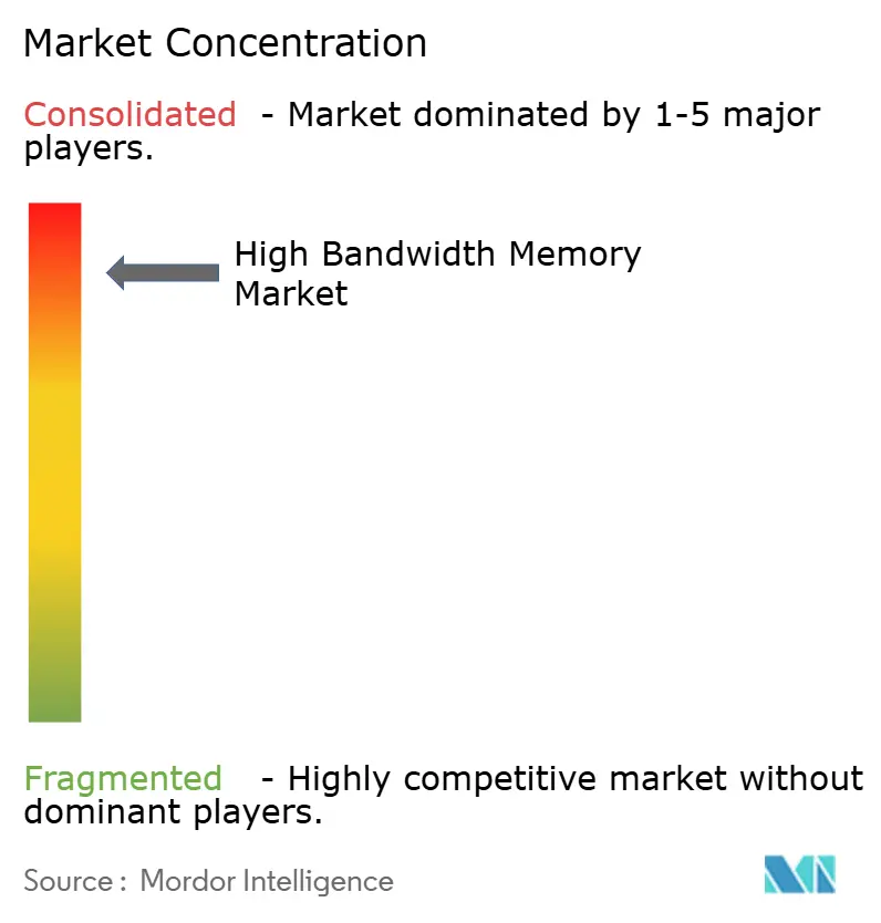
Competition centers on a concentrated group of memory producers, supported by specialized foundry and assembly capabilities. Micron Technology, Inc., Samsung Electronics Co., Ltd., and SK hynix Inc. produce HBM. Taiwan Semiconductor Manufacturing Company Limited provides advanced packaging, while ASE Technology Holding Co., Ltd. participates through packaging and testing businesses. Samsung began HBM4 mass production and shipped commercial products to customers in February 2026. Samsung's commercial shipments gave system designers an HBM4 supply option for volume programs, so competition extends beyond product sampling to production execution.
In January 2026, Yonhap, citing unnamed sources, reported that NVIDIA had allocated about 70% of its 2026 HBM4 demand for the Vera Rubin platform to SK hynix. SK hynix had completed HBM4 development and announced mass-production readiness in September 2025. The reported allocation turns the competitive question from readiness alone toward how much of a particular platform's requirement a supplier can serve. The balance of that requirement leaves an opening for competing suppliers within the same cycle, alongside the concentrated sourcing relationship reported for SK hynix.
Panel-based packaging offers an additional competitive route for integrating HBM with compute devices. In May 2026, Advanced Semiconductor Engineering, a member of ASE Technology Holding, announced an automated 310 mm × 310 mm panel-level packaging line for heterogeneous integration involving HBM. ASE said the line enables a transition from wafer-level to panel-level packaging while preserving design-rule consistency across FOCoS and FOCoS-Bridge. On July 30, 2026, management targeted production by Q1 2027. Until the line starts production, its panel-format packaging is a planned option for system designers.
High Bandwidth Memory Industry Leaders
-
Micron Technology, Inc.
-
Samsung Electronics Co., Ltd.
-
SK hynix Inc.
-
Taiwan Semiconductor Manufacturing Company Limited
-
ASE Technology Holding Co., Ltd.
- *Disclaimer: Major Players sorted in no particular order
High Bandwidth Memory Market Companies Covered in this Report
- Samsung Electronics Co., Ltd.
- SK hynix Inc.
- Micron Technology, Inc.
- Intel Corporation
- Advanced Micro Devices, Inc.
- NVIDIA Corporation
- Taiwan Semiconductor Manufacturing Company Limited
- ASE Technology Holding Co., Ltd.
- Amkor Technology, Inc.
- Powertech Technology Inc.
- United Microelectronics Corporation
- GlobalFoundries Inc.
- Applied Materials, Inc.
- Marvell Technology, Inc.
- Rambus Inc.
- Cadence Design Systems, Inc.
- Synopsys, Inc.
- Siliconware Precision Industries Co., Ltd.
- JCET Group Co., Ltd.
- Chipbond Technology Corporation
- Broadcom Inc.
- Celestial AI
- ASE-SPIL (Silicon Products)
- Graphcore Limited
Key Opportunities for Market Participants
The opportunities compare volume supply, custom-memory development and AI-factory integration as different routes into expanding accelerator infrastructure. In August 2026, AWS announced plans to deploy 2 million additional NVIDIA Blackwell Ultra, Rubin and Rubin Ultra GPUs across its global infrastructure, including AI factories, in 2027-2028. NVIDIA also announced that Amazon's Annapurna Labs will be the first to work on NVHBM within their NVLink Fusion collaboration. The deployment plan creates a potential volume pathway, while the custom-memory collaboration creates an earlier-stage design and validation pathway.
Market Opportunities Table of High Bandwidth Memory Market
| Opportunity | Why now | Buyer / lead segment | Recommended play | Main barrier | Likely beneficiaries |
|---|---|---|---|---|---|
| HBM supply for cloud GPU expansion | Multi-generation infrastructure rollout planned for 2027-2028 | GPU platform suppliers serving cloud operators | Align qualified HBM output with accelerator shipment schedules | Synchronizing memory output with system deployment | Qualified HBM producers and NVIDIA |
| Custom HBM for AI ASIC designs | NVHBM collaboration and memory-partner validation pathway announced | Custom-chip designers such as Annapurna Labs | Develop and validate memory with the chip-design partner | Validation before commercialization | Participating memory vendors, Annapurna Labs and NVIDIA |
| HBM configurations for AI-factory systems | AI factories included in the planned infrastructure expansion | AI-factory system integrators | Offer HBM configurations through complete-system partnerships | Coordinating memory and accelerator integration | HBM suppliers aligned with AI-factory system vendors |
| Source: Mordor Intelligence | |||||
The central opening is a design position with the memory partners that will validate NVHBM ahead of commercialization. The AWS plan identifies GPU generations, while NVHBM validation by unnamed memory partners leaves the memory supply position open at the design stage. Neither announcement allocates HBM demand to a named supplier, so validation work offers an entry point for competing over a future design position.
Recent Industry Developments in High Bandwidth Memory Market
- Sep 2026: Micron Technology, Inc. reported that cleanroom preparation at its Singapore HBM advanced-packaging facility was ahead of plan, with initial output expected in early calendar 2027.
- Aug 2026: SK hynix Inc. held a groundbreaking ceremony in West Lafayette, Indiana, for an HBM advanced-packaging and testing facility, with wafers to be supplied from South Korea.
- Aug 2026: NVIDIA announced that Amazon's Annapurna Labs will be the first to work on NVHBM within their NVLink Fusion collaboration.
High Bandwidth Memory Market Report Scope and Research Methodology
Market Definition and Coverage
The high bandwidth memory market measures annual supplier revenue from sales of stacked high-bandwidth memory devices across Global markets. The sales are classified by end application, HBM generation, stack capacity, processor interface, and geography.
Scope exclusions: Non-HBM memory devices, including DDR, GDDR, and LPDDR, processors, accelerators, servers, networking equipment, consumer electronics, and vehicles sold as finished products, and separately sold packaging services, interposers, production equipment, and HBM manufacturing inputs are excluded.
Segments Covered in This Report
- By Application
- Servers
- Networking
- High-Performance Computing
- Consumer Electronics
- Automotive and Transportation
- By Technology
- HBM2
- HBM2E
- HBM3
- HBM3E
- HBM4
- By Memory Capacity per Stack
- 4 GB
- 8 GB
- 16 GB
- 24 GB
- 32 GB and Above
- By Processor Interface
- GPU
- CPU
- AI Accelerator / ASIC
- FPGA
- Others
- By Geography
- North America
- United States
- Canada
- Mexico
- South America
- Brazil
- Rest of South America
- Europe
- Germany
- France
- United Kingdom
- Rest of Europe
- Asia-Pacific
- China
- Japan
- India
- South Korea
- Rest of Asia-Pacific
- Middle East and Africa
- Middle East
- Saudi Arabia
- United Arab Emirates
- Turkey
- Rest of Middle East
- Africa
- South Africa
- Rest of Africa
- Middle East
- North America
Data Sources, Market Sizing, and Validation
Desk Research
Desk research would use public sources such as World Semiconductor Trade Statistics forecasts to frame memory and semiconductor cycles, NVIDIA product specifications to check HBM capacity and bandwidth in accelerator configurations, and Samsung and SK hynix newsrooms and financial disclosures to check product ramps, shipment timing, stack generations, and supplier commentary. Together, these sources help distinguish HBM-specific signals from broader DRAM, packaging, and accelerator trends and provide dated evidence for changes in product mix and supply.
Company filings, annual reports, earnings materials, and reputable semiconductor press would add financial context and cross-check shipment, capacity, and customer-program evidence against the public series. The named sources are illustrative rather than exhaustive, and further sources inform collection, validation and clarification.
Primary Interviews and Surveys
Primary research would draw on interviews with HBM supplier executives and managers, memory product and sales leaders, packaging and foundry specialists, accelerator and system procurement leaders, and regional channel experts. Interview questions would test secondary evidence on shipments, stack generations, realized pricing, customer qualification, and capacity constraints, while clarifying whether reported revenue is attributable to finished HBM stacks. Where answers differ or evidence is incomplete, analysts would record the unresolved item, seek corroborating evidence from another role or public record, and use triangulation to retain only supportable assumptions in the model.
Distribution of primary research fieldwork respondents
| Company type | Respondent position | Region |
|---|---|---|
| Top tier: 30% | CXOs: 20% | APAC: 45% |
| Mid tier: 45% | Functional/Unit leaders: 35% | EMEA: 25% |
| Smaller Players: 25% | Managers: 45% | Americas: 30% |
Market-Sizing & Forecasting
The model starts top down with global supplier revenue attributable to finished HBM stacks, then estimates the 2026 share mix and forecasts the same USD revenue basis through 2032. Key indicators include AI server and accelerator deployments, HBM content per processor, generation and capacity mix, supplier shipment and revenue disclosures, and advanced-packaging availability. These indicate demand, revenue per system, product mix, and the amount of output that can reach customers. Using disclosed product placements, customer programs, supplier commentary, and regional demand evidence, analysts allocate totals across application, technology, stack-capacity, processor-interface, and regional categories, then check selected supplier totals and sampled average selling price times volume against the market estimate.
For forecasts, scenario analysis can vary accelerator deployments, HBM content, generation transitions, pricing, and shipment constraints, with time-series smoothing applied where a stable series supports it. Where a supplier or segment lacks a direct observation, analysts use the nearest documented shipment, product configuration, or pricing indicator and record the assumption for sensitivity checks rather than treating an unsupported value as observed. Interview evidence would test the direction and practical limits of these variable-level forecasts, while disagreements would remain visible as alternative scenarios until independent evidence resolves them.
Data Validation & Update Cycle
Before accepting a figure, analysts check the HBM product, revenue basis, year, and geography against supplier filings, product announcements, market series, shipment and pricing signals, and accelerator configurations. They investigate outliers, reconcile totals and segment shares, compare forecast changes with independent demand and supply indicators, and document each adjustment before a second analyst reviews the calculations and source trail. Re-contact is triggered when a material answer conflicts with a new filing, product ramp, or independently observed market signal. The model is refreshed annually, reviewed between cycles after material supply, product, or trade events, and given a fresh source and calculation pass immediately before delivery.
Mordor Intelligence's High Bandwidth Memory Market Sizing Compared With Other Published Estimates
The high bandwidth memory market measures annual supplier revenue from sales of stacked high-bandwidth memory devices across Global markets. Using disclosed product placements, customer programs, supplier commentary, and regional demand evidence, analysts allocate totals across application, technology, stack-capacity, processor-interface, and regional categories, then check selected supplier totals and sampled average selling price times volume against the market estimate.
Key Gap Drivers are addressed through a consistent transaction boundary, market-specific demand inputs and cross-checks across the study. Before accepting a figure, analysts check the HBM product, revenue basis, year, and geography against supplier filings, product announcements, market series, shipment and pricing signals, and accelerator configurations.
Benchmark comparison
| Source | Market Size | Gaps in Research Methodology |
|---|---|---|
| Mordor Intelligence | USD 5 B (2027) | |
| Global Market Research Publisher A | USD 50.5 B (2026) | At its 2026 base, this estimate is 910.0% above this report's 2027 value of USD 5 B, 1 year later. |
| Global Market Research Publisher B | USD 8.67 B (2026) | At its 2026 base, this estimate is 73.4% above this report's 2027 value of USD 5 B, 1 year later. |
Mordor Intelligence ties the estimate to the study’s defined coverage and demand model. Before accepting a figure, analysts check the HBM product, revenue basis, year, and geography against supplier filings, product announcements, market series, shipment and pricing signals, and accelerator configurations.
Key Questions Answered in the Report
What is the High Bandwidth Memory market size and growth outlook?
The market is expected to reach USD 5 billion in 2027 and USD 15.99 billion by 2032, with a 26.18% CAGR over 2027-2032.
What drives demand for HBM?
Cloud infrastructure expansion and larger stack configurations support demand. In less than a year through March 2026, Microsoft deployed hundreds of thousands of liquid-cooled Grace Blackwell GPUs across its global data-center footprint.
Which application has the largest HBM share?
Servers held a 68.13% share in 2026, leading the application segments.
Which companies lead the HBM industry?
Major participants include Micron Technology, Inc., Samsung Electronics Co., Ltd., SK hynix Inc., Taiwan Semiconductor Manufacturing Company Limited and ASE Technology Holding Co., Ltd.
What could limit the HBM outlook?
Taller-stack yield risk and packaging constraints can restrict usable output. In October 2026, TSMC reported a small back-end capacity shortage.
Which region leads the HBM industry?
Asia-Pacific led with a 41.31% share in 2026 and is forecast to grow at a 26.9% CAGR over 2027-2032, the fastest regional pace.