Flip Chip Technology Market Size and Share
Market Overview
| Study Period | 2020 - 2031 |
|---|---|
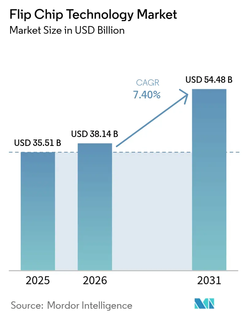
| Market Size (2026) | USD 38.14 Billion |
| Market Size (2031) | USD 54.48 Billion |
| Growth Rate (2026 - 2031) | 7.40% CAGR |
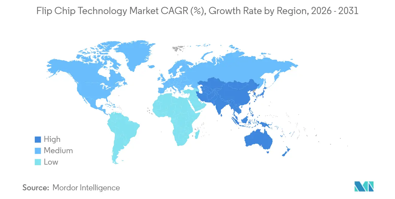
| Fastest Growing Market | Asia-Pacific |
| Largest Market | Asia-Pacific |
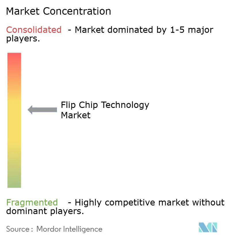
| Market Concentration | Medium |
Major Players *Disclaimer: Major Players sorted in no particular order Image © Mordor Intelligence. Reuse requires attribution under CC BY 4.0. | |
Flip Chip Technology Market Analysis by Mordor Intelligence
The flip chip technology market size was valued at USD 35.51 billion in 2025 and estimated to grow from USD 38.14 billion in 2026 to reach USD 54.48 billion by 2031, at a CAGR of 7.40% during the forecast period (2026-2031). Growth mirrored the semiconductor industry’s transition to chiplet-based architectures that required dense, thermally efficient interconnects. AI data-center build-outs pushed high-bandwidth memory packaging to the fore, while copper-pillar and hybrid bonding lines addressed the fine-pitch needs that traditional solder bumps could not meet. Foundries entered the packaging arena, accelerating vertical integration and bringing new competitive pressures on outsourced assembly and test providers. Asia-Pacific retained scale advantages, yet supply-chain de-risking programs in North America and Europe triggered large green-field investments in advanced packaging facilities.
Key Report Takeaways
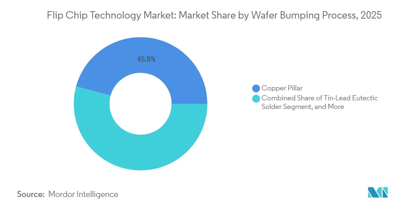
- By wafer bumping process, copper pillar held 45.78% revenue share in 2025, while Cu-to-Cu hybrid bonding is projected to expand at 9.55% CAGR through 2031.
- By packaging technology, FC-BGA led with 37.62% share in 2025, while fan-out WLP/panel-level solutions are forecast to grow at 9.88% CAGR to 2031.
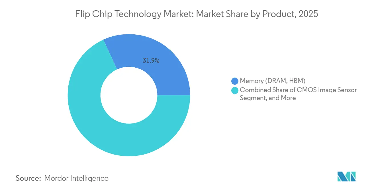
- By product, memory accounted for 31.85% of the flip chip technology market share in 2025, whereas the GPU/AI accelerator segment is set to advance at 12.45% CAGR to 2031.
- By end-use industry, consumer electronics and wearables held a 28.96% share in 2025, while data-center and cloud applications are expected to log a 8.86% CAGR through 2031.
- By geography, Asia-Pacific captured 53.92% of 2025 revenue and is projected to post a 9.22% CAGR through 2031.
Note: Market size and forecast figures in this report are generated using Mordor Intelligence’s proprietary estimation framework, updated with the latest available data and insights as of 2026.
Global Flip Chip Technology Market Trends and Insights
Drivers Impact Analysis*
| Driver | (~) % Impact on CAGR Forecast | Geographic Relevance | Impact Timeline |
|---|---|---|---|
| Surge in heterogeneous integration demand (AI/HPC) | +2.1% | Global, concentrated in North America and Asia-Pacific | Medium term (2-4 years) |
| Rising adoption of copper-pillar and micro-bump interconnects | +1.8% | Asia-Pacific core, expanding to North America and Europe | Short term (≤ 2 years) |
| Wearables and IoT miniaturization push | +1.2% | Global, with early adoption in Asia-Pacific and North America | Long term (≥ 4 years) |
| Automotive ADAS/EV reliability requirements | +1.0% | Global, led by Europe and North America | Medium term (2-4 years) |
| Glass-core substrate commercial trials | +0.9% | North America and Asia-Pacific, pilot programs in Europe | Long term (≥ 4 years) |
| Demand for chiplet-ready Cu-to-Cu hybrid bonding | +0.8% | Asia-Pacific core, expanding globally | Medium term (2-4 years) |
| Source: Mordor Intelligence | |||


Surge in Heterogeneous Integration Demand (AI/HPC)
Chipmakers pivoted from 2D scaling to heterogeneous integration that joined multiple chiplets in a single package, lifting demand for fine-pitch Cu-to-Cu interconnects.[1]Applied Materials, “Hybrid Bonding,” appliedmaterials.com TSMC’s plan to boost CoWoS capacity to 1.31 million units by 2026 illustrated how GPU vendors such as Nvidia shaped the flip chip technology market. The approach enhanced bandwidth while lowering power compared with legacy bumps, supporting the performance roadmap for AI accelerators.
Rising Adoption of Copper-Pillar and Micro-Bump Interconnects
Copper-pillar bumps delivered superior electrical resistance and reliability, explaining their 46.3% 2024 revenue share. High-speed plating chemistries from DuPont provided uniform thickness control essential for sub-40 µm pitches. The shift eroded tin-lead dominance and paved the way for 3D integration schemes that underpin the flip chip technology market.
Wearables and IoT Miniaturization Push
System-in-package and wafer-level chip-scale methods became staples for smart watches and health trackers that demanded slim profiles without sacrificing battery life. Ultra-HDI PCB advances using modified semi-additive processing and laser direct imaging offered trace widths below 40 µm, enabling compact sensor modules.
Automotive ADAS/EV Reliability Requirements
Autonomous driving and power-train electrification require packages that survive temperatures above 200 °C. Automotive-grade flip chip lines employed high-temperature underfills and copper pillar joints qualified for AEC-Q100 Grade 0. JCET’s automotive electronics revenue expanded at more than 50% CAGR between 2019 and 2023, signaling rapid adoption of these robust processes.
Restraints Impact Analysis*
| Restraint | (~) % Impact on CAGR Forecast | Geographic Relevance | Impact Timeline |
|---|---|---|---|
| High capital intensity of advanced bumping lines | -1.4% | Global, most pronounced in North America and Europe | Short term (≤ 2 years) |
| Lead-free reliability and warpage challenges | -0.9% | Global, regulatory pressure is strongest in Europe | Medium term (2-4 years) |
| Sub-10 µm alignment yield losses | -0.7% | Asia-Pacific core, expanding to global advanced fabs | Short term (≤ 2 years) |
| Supply-chain exposure to critical metal chemicals | -0.5% | Global, concentrated risk in North America and Asia-Pacific | Medium term (2-4 years) |
| Source: Mordor Intelligence | |||
High Capital Intensity of Advanced Bumping Lines
Scaling to sub-10 µm pitches required lithography steppers, advanced sputter tools, and plasma cleaners that pushed line cost above USD 250 million per module. TSMC earmarked USD 90 billion for dedicated packaging plants, underscoring the entry hurdle for smaller competitors. Collaborative R&D programs such as 3M’s participation in the US-JOINT consortium aimed to spread risk across the supply chain.
Lead-Free Reliability and Warpage Challenges
RoHS mandates accelerated SnAgCu adoption, yet differential thermal expansion introduced warpage and solder fatigue in flip chip stacks. Studies showed that eutectic Sn-Bi joints extended thermal-cycling life but suffered brittleness that limited high-stress applications. Low-temperature reflow at 175 °C reduced head-on-pillow defects but required bismuth-based alloys that complicated high-volume assembly.
*Our forecasts treat driver/restraint impacts as directional, not additive. The impact forecasts reflect baseline growth, mix effects, and variable interactions.
Segment Analysis
By Wafer Bumping Process: Copper Dominance Drives Innovation
Copper pillar technology held 45.78% revenue in 2025 within the flip chip technology market. The segment benefited from reduced resistance and heightened current-carrying capability. The flip chip technology market size for Cu-to-Cu hybrid bonding is projected to expand at a 9.55% CAGR as chiplet adoption grows. The hybrid method lowered inter-chip spacing to 0.8 µm, far beyond solder’s physical limits. Tin-lead solutions still served legacy nodes, whereas gold-stud bumps remained confined to aerospace.
Advances in electroplated chemistries sustained pillar height uniformity below 2%, a prerequisite for 3D stacks. IEEE research validated solder-free Cu-Cu bonding at 260 °C as a manufacturable path for heterogeneous integration. Innovations positioned copper formats to absorb share from both lead-free and precious-metal alternatives.


By Packaging Technology: Advanced Architectures Reshape Market Dynamics
FC-BGA commanded 37.62% of 2025 revenue thanks to proven reliability in servers. Fan-out WLP and panel-level formats are expected to record a 9.88% CAGR, catalyzed by AI accelerators demanding large body sizes. ASE allocated USD 200 million to 310 mm × 310 mm panels that promise sevenfold usable area over wafers, a cost breakthrough. The flip chip technology market size for panel-level packages will climb as line yields improve.
Specialty flows such as CoWoS and EMIB enable HBM stacking essential for AI training units. IBM and Intel pursued glass-substrate roadmaps that offer lower warpage and higher line-space ratios than organic laminates. 3D IC with TSV remained a niche for extreme bandwidth-class devices due to high cost and process complexity, but set the ceiling on attainable performance.
By Product: Memory and AI Accelerators Lead Growth
Memory held a 31.85% share in 2025 as HBM adoption soared. Applied Materials estimated sixfold growth in HBM packaging revenue, driven by 19 additional process steps versus conventional DRAM. GPU/AI accelerators will post a 12.45% CAGR to 2031. The flip chip technology market quickly adapted to combine multiple HBM stacks with logic nodes through interposers, creating package power densities exceeding 1 kW.
CMOS image sensors maintained momentum on the back of multi-camera smartphones, while micro-LED dies required sub-20 µm bumping that dovetailed with copper pillar capabilities. Silicon Box’s USD 3.5 billion Italian line targeting chiplet solutions illustrated regional investment in cross-product synergies.
By End-Use Industry: Data Centers Drive Transformation
Consumer electronics kept a 28.96% share but slowed as handset volumes plateaued. Data center and cloud demand will grow at 8.86% CAGR because AI inference nodes deploy high-bandwidth chiplets in volume. The flip chip technology market size for data-center applications is projected to widen rapidly as servers adopt four- and eight-HBM configurations.
Automotive electronics leveraged copper pillar joints molded with high-glass-transition underfills to meet Grade 0 temperature swings. Medical implants benefited from biocompatible wafer-level packages that embedded wireless telemetry while keeping envelope size minimal.Telecommunications rolled out millimeter-wave 5G radios that required low-loss interconnects compatible with Cu-pillar bumps.
Geography Analysis
Asia-Pacific held 53.92% of 2025 revenue. The region housed the bulk of wafer fabs and retained cost advantages, sustaining the largest slice of the flip chip technology market. Government incentives supported next-node R&D, yet export-control actions induced leading firms to build parallel capacity offshore. North America accelerated foundry and packaging startups under the CHIPS Act, adding resilience and creating a local demand pull. The flip chip technology market share for North America is expected to rise modestly as Arizona and Texas campuses come online.
Europe pursued technology sovereignty through the European Chips Act and directed capital toward panel-level and glass-core substrate lines. Silicon Box’s Novara facility is slated to process 10,000 panels weekly by 2028, anchoring a regional ecosystem. Middle East and Africa remained early-stage but benefited from electronics final-assembly hubs that feed into global supply chains.
Supply-chain diversification scattered future investments across at least three continents, muting single-region dominance. However, Asia-Pacific still boasted unmatched engineering depth, keeping it the reference center for high-volume manufacturing.

Competitive Landscape
Foundry vertical integration re-shaped rivalry. TSMC combined wafer production with CoWoS back-end services, shortening customer cycle time. ASE responded with panel-level builds and auto-grade qualifications to safeguard the share. Intel exited internal glass substrate R&D and partnered with specialist suppliers, validating the complexity hurdle for new entrants.[4]TechPowerUp, “Intel Abandons In-House Glass Substrate R&D,” techpowerup.com
Hybrid bonding patents created defensible moats. IBM reduced inter-chip spacing to 0.8 µm, enabling dramatic bandwidth gains. Material vendors such as DuPont and 3M are advancing chemistries for pillar plating and low-warpage dielectric films, embedding themselves deeper into the value chain. Chinese OSATs expanded capacity with multi-billion-dollar plants, but technology parity with leading nodes remained a moving target.
Market leaders are increasingly differentiated by advanced node readiness rather than total bump count. The shift sharpened consolidation pressure on mid-tier players lacking capital to upgrade sub-10 µm lines, catalyzing mergers aimed at pooling R&D and customer bases.
Flip Chip Technology Industry Leaders
Amkor Technology Inc.
UTAC Holdings Ltd
Taiwan Semiconductor Manufacturing Co. (TSMC)
Chipbond Technology Corporation
TF-AMD Microlectronics Sdn Bhd.
- *Disclaimer: Major Players sorted in no particular order

Recent Industry Developments
- July 2025: TSMC reorganized its USD 65 billion Arizona project to address cost overruns while retaining advanced packaging modules.
- May 2025: TSMC outlined USD 42 billion in 2025 capital spending covering eight wafer fabs and one packaging plant.
- April 2025: TSMC announced a NT$1.5 trillion (USD 45.2 billion) expansion in Kaohsiung focused on 2 nm wafer and advanced packaging capacity.
- February 2025: 3M joined the US-JOINT consortium, opening a Silicon Valley lab to co-develop advanced packaging materials.


Global Flip Chip Technology Market Report Scope
Flip-chip technology is one of the oldest and most widely used techniques for semiconductor packaging. Flip-chip was originally introduced by IBM 30 years ago. Nevertheless, it is keeping up with the times and developing new bumping solutions to serve advanced technologies such as 2.5D and 3D. Flip chip is used for traditional applications, such as Laptops, Desktops, CPU, GPU, chipsets, etc.
| Copper Pillar |
| Tin-Lead Eutectic Solder |
| Lead-Free Solder (SnAg, SAC, etc.) |
| Gold-Stud Bumping |
| Cu-to-Cu Hybrid / Direct Bond |
| FC-BGA (2D/2.1D/2.5D/3D) |
| FCCSP / CSP |
| CoWoS / InFO / EMIB |
| Fan-Out WLP / PLP |
| 3D IC with TSV |
| Memory (DRAM, HBM) |
| CMOS Image Sensor |
| LED and Mini/Micro-LED |
| SoC / Application Processor |
| GPU / AI Accelerator |
| CPU / Server Processor |
| Consumer Electronics and Wearables |
| Automotive and Transportation |
| Industrial and Robotics |
| Telecommunications and 5G Infrastructure |
| Data Center and Cloud |
| Military and Aerospace |
| Medical and Healthcare Devices |
| North America | United States | |
| Canada | ||
| Mexico | ||
| South America | Brazil | |
| Rest of South America | ||
| Europe | Germany | |
| France | ||
| United Kingdom | ||
| Russia | ||
| Rest of Europe | ||
| Asia-Pacific | China | |
| Taiwan | ||
| South Korea | ||
| Japan | ||
| Malaysia | ||
| Singapore | ||
| Rest of Asia-Pacific | ||
| Middle East and Africa | Middle East | Turkey |
| Rest of Middle East | ||
| Africa | South Africa | |
| Rest of Africa | ||
| By Wafer Bumping Process | Copper Pillar | ||
| Tin-Lead Eutectic Solder | |||
| Lead-Free Solder (SnAg, SAC, etc.) | |||
| Gold-Stud Bumping | |||
| Cu-to-Cu Hybrid / Direct Bond | |||
| By Packaging Technology | FC-BGA (2D/2.1D/2.5D/3D) | ||
| FCCSP / CSP | |||
| CoWoS / InFO / EMIB | |||
| Fan-Out WLP / PLP | |||
| 3D IC with TSV | |||
| By Product | Memory (DRAM, HBM) | ||
| CMOS Image Sensor | |||
| LED and Mini/Micro-LED | |||
| SoC / Application Processor | |||
| GPU / AI Accelerator | |||
| CPU / Server Processor | |||
| By End-Use Industry | Consumer Electronics and Wearables | ||
| Automotive and Transportation | |||
| Industrial and Robotics | |||
| Telecommunications and 5G Infrastructure | |||
| Data Center and Cloud | |||
| Military and Aerospace | |||
| Medical and Healthcare Devices | |||
| By Geography | North America | United States | |
| Canada | |||
| Mexico | |||
| South America | Brazil | ||
| Rest of South America | |||
| Europe | Germany | ||
| France | |||
| United Kingdom | |||
| Russia | |||
| Rest of Europe | |||
| Asia-Pacific | China | ||
| Taiwan | |||
| South Korea | |||
| Japan | |||
| Malaysia | |||
| Singapore | |||
| Rest of Asia-Pacific | |||
| Middle East and Africa | Middle East | Turkey | |
| Rest of Middle East | |||
| Africa | South Africa | ||
| Rest of Africa | |||


Key Questions Answered in the Report
What is the current value of the flip chip technology market?
The global flip chip technology market was valued at USD 38.14 billion in 2026.
How fast is the flip chip technology market expected to grow?
Between 2026 and 2031, the market is projected to register a 7.40% CAGR.
Which wafer bumping process leads the market?
Copper pillar bumping held 45.78% revenue share in 2025, reflecting its superior electrical performance.
Why is AI driving demand for advanced packaging?
AI accelerators require high-bandwidth memory stacks and fine-pitch interconnects that only advanced flip chip packages can deliver.
Which region dominates the flip chip technology market?
Asia-Pacific captured 53.92% of 2025 revenue, supported by extensive wafer-fabrication and packaging capacity.
What is the fastest-growing end-use industry?
Data-center and cloud applications are forecast to grow at 8.86% CAGR through 2031 as AI workloads expand.
Page last updated on:


