Dielectric Etchers Market Size and Share
Market Overview
| Study Period | 2020 - 2031 |
|---|---|
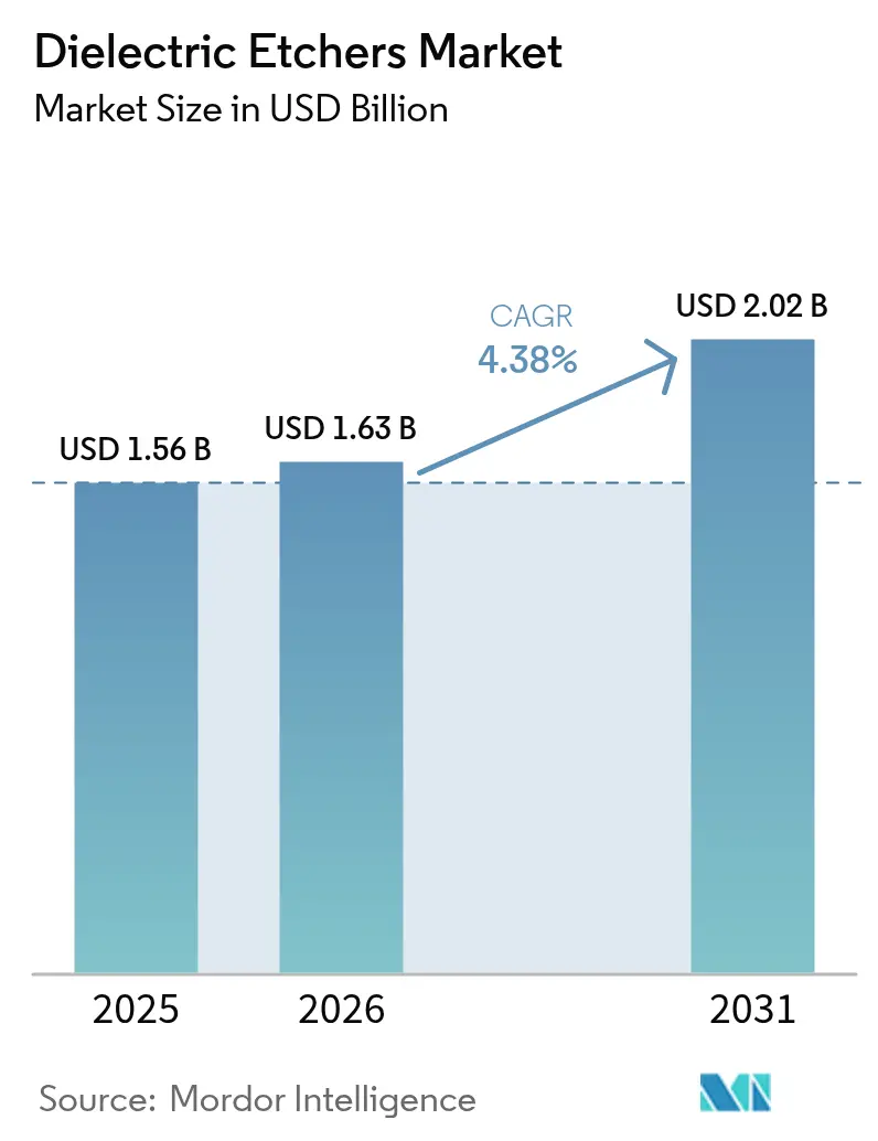
| Market Size (2026) | USD 1.63 Billion |
| Market Size (2031) | USD 2.02 Billion |
| Growth Rate (2026 - 2031) | 4.38% CAGR |
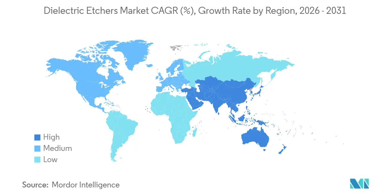
| Fastest Growing Market | Middle East |
| Largest Market | Asia Pacific |
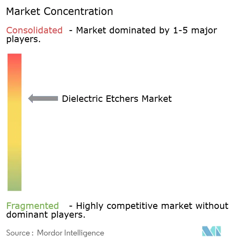
| Market Concentration | Medium |
Major Players *Disclaimer: Major Players sorted in no particular order Image © Mordor Intelligence. Reuse requires attribution under CC BY 4.0. | |
Dielectric Etchers Market Analysis by Mordor Intelligence
The dielectric etchers market size is expected to increase from USD 1.56 billion in 2025 to USD 1.63 billion in 2026 and reach USD 2.02 billion by 2031, growing at a CAGR of 4.38% over 2026-2031. The measured headline growth conceals a rapid pivot toward atomic-layer and cryogenic platforms as gate-all-around logic and 3D NAND stacks with more than 300 layers demand angstrom-level depth control. Asia-Pacific pure-play foundries continue to anchor global equipment spending, but North American and European subsidy programs are reshaping regional capacity plans. Memory makers’ push to 400-plus layers is enlarging tool content per wafer, while packaging houses are ordering specialty systems for chiplet redistribution layers. At the same time, looming fluorinated-gas regulations and capital-expenditure cyclicality introduce downside risks that equipment vendors must hedge through service contracts and diversified customer mixes. These cross-currents ensure that the dielectric etchers market will outgrow overall wafer-fab equipment while remaining sensitive to node transitions and subsidy disbursements.
Key Report Takeaways
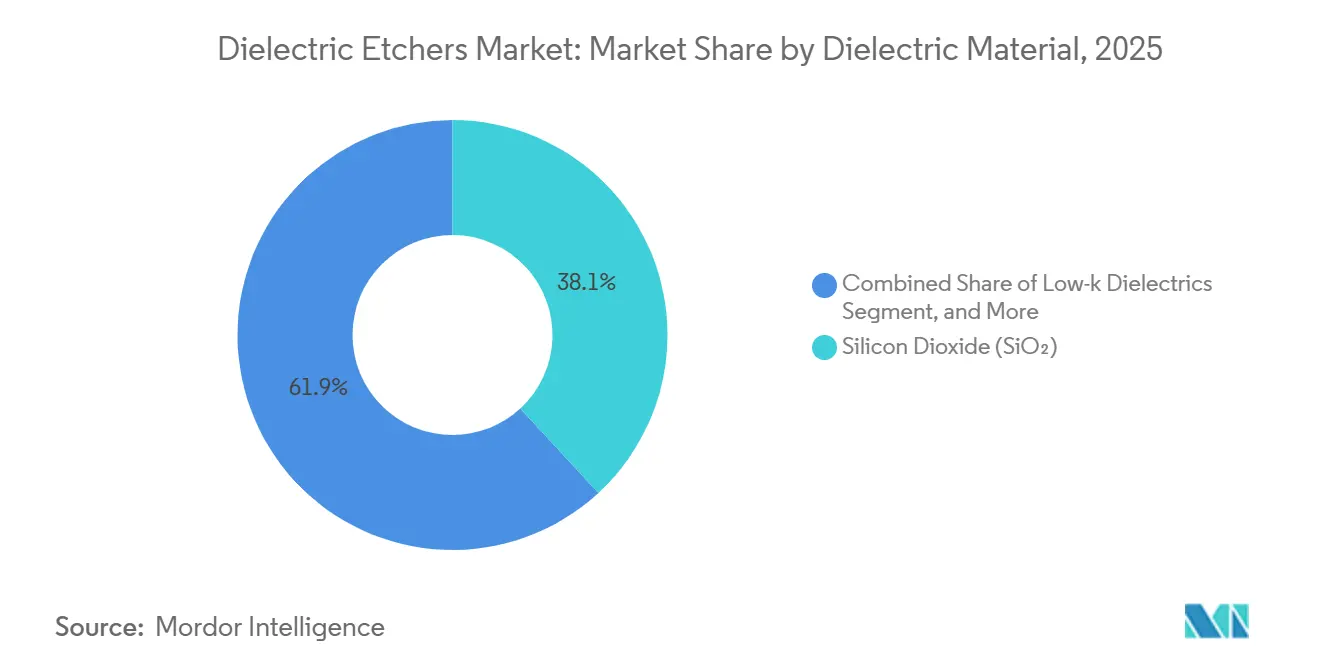
- By dielectric material, silicon dioxide led with 38.13% of dielectric etchers market share in 2025, while low-k dielectrics are projected to expand at a 6.12% CAGR through 2031.
- By technology, inductively-coupled plasma systems commanded a 34.16% share of the dielectric etchers market size in 2025 and atomic-layer etching is advancing at a 6.04% CAGR over 2026-2031.
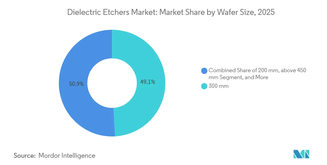
- By wafer size, 300-millimeter platforms accounted for 49.12% of the dielectric etchers market size in 2025, whereas ≥450-millimeter tools are forecast to rise at a 5.83% CAGR to 2031.
- By end user, pure-play foundries held 42.83% of dielectric etchers market share in 2025, while R&D and pilot lines represent the fastest-growing segment with a 5.92% CAGR to 2031.
- By geography, Asia-Pacific captured 56.94% revenue in 2025, and the Middle East is projected to post a 4.82% CAGR through 2031.
Note: Market size and forecast figures in this report are generated using Mordor Intelligence’s proprietary estimation framework, updated with the latest available data and insights as of 2026.
Global Dielectric Etchers Market Trends and Insights
Drivers Impact Analysis*
| Driver | (~) % Impact on CAGR Forecast | Geographic Relevance | Impact Timeline |
|---|---|---|---|
| Proliferation of Sub-7 nm Logic Nodes | +1.2% | Asia-Pacific core, North America foundry expansions | Medium term (2-4 years) |
| 3D NAND Layer-Count Escalation | +1.0% | Asia-Pacific (Korea, Japan, China), selective North America | Medium term (2-4 years) |
| Low-k Dielectric Adoption in Advanced Packaging | +0.8% | Global, concentration in Taiwan, Korea, United States | Short term (≤ 2 years) |
| Rising 5G and AI Chip Volumes | +0.9% | Global, led by Asia-Pacific manufacturing hubs | Short term (≤ 2 years) |
| Transition to Atomic-Layer Etching | +0.7% | Taiwan, Korea, United States, Europe | Long term (≥ 4 years) |
| Government-Funded Fab Localization Programs | +0.6% | North America, Europe, India, Middle East | Long term (≥ 4 years) |
| Source: Mordor Intelligence | |||
Poliferation of Sub-7 nm Logic Nodes
Gate-all-around transistor architectures at 2-nanometer and 3-nanometer nodes require dielectric removal with angstrom-level precision to protect nanosheet channels. Taiwan Semiconductor Manufacturing Company’s January 2026 ramp of 2-nanometer production exemplifies the demand surge for next-generation etchers.[1]Jane Doe, “TSMC Kicks Off Mass Production of 2 nm Chips,” Reuters, reuters.com Samsung’s USD 17 billion Taylor, Texas investment will add further logic capacity by late 2026. Intel’s planned 18A node featuring backside power rails pushes selective-dielectric-etch requirements into 2027.[2]Intel, “Intel 18A Process Technology,” intel.com Tool vendors are embedding real-time metrology and machine-learning algorithms to tune plasma parameters wafer by wafer, lifting average selling prices and extending qualification timelines. Consequently, the dielectric etchers market continues to tilt toward capital-intensive platforms that only leading foundries can afford.
3D NAND Layer-Count Escalation
Memory producers surpassed the 300-layer threshold in 2025 and aim to exceed 400 layers by late 2026, driving demand for channel-hole etching beyond 15 micrometers depth with sub-50 nm diameters.[3]SK Hynix, “SK Hynix Starts Mass Production of 321-Layer NAND,” skhynix.com Lam Research’s Cryo 3.0 platform cools wafers to cryogenic temperatures, suppressing sidewall bowing while improving throughput by 2.5×, a capability Samsung will exploit for V10 NAND. Micron’s USD 100 billion New York program adds a multiyear tailwind as its first fab comes online in 2028. Atomic-layer etching is indispensable for staircase and word-line formation, minimizing critical-dimension variation across hundreds of layers. Capital intensity—exceeding USD 10 million per chamber—concentrates orders among the top three memory makers, reinforcing supplier pricing power within the dielectric etchers market.
Low-k Dielectric Adoption in Advanced Packaging
Chiplet interconnects and high-bandwidth memory stacks rely on low-k films below k = 2.5, demanding plasma chemistries that prevent pore collapse and residue build-up. Lam Research’s Kiyo etcher, launched in October 2025, halts precisely on copper barriers without manual endpoint detection, raising yields in sub-2 µm vias. Intel’s Foveros Direct technology bonds dies at 10 µm bump pitch, leveraging selective dielectric etch to form micro-vias. Outsourced assembly houses are now buying front-end-grade etchers to capture value-added services, intensifying competition. As packaging volumes rise, this sub-segment is forecast to outpace wafer-front-equipment growth, further supporting the dielectric etchers market.
Rising 5G and AI Chip Volumes
Artificial-intelligence accelerators and 5G infrastructure are pushing foundry utilization toward record highs. Taiwan Semiconductor Manufacturing Company plans USD 30 billion-plus 2026 capex with more than half earmarked for AI-centric nodes. Nvidia, Google, and Samsung demand low-resistance vias etched with minimal sidewall damage to sustain power-delivery targets. Edge AI devices based on 7 nm and 5 nm designs require similar dielectric precision, widening the customer base. Gallium-nitride power amplifiers for 5G use inductively-coupled or microwave plasmas that avoid lattice damage. Multi-year purchase commitments from logic customers have improved vendor revenue visibility, reinforcing a structurally healthier dielectric etchers market than prior memory-led cycles.
Restraints Impact Analysis*
| Restraints | (~) % Impact on CAGR Forecast | Geographic Relevance | Impact Timeline |
|---|---|---|---|
| High Capital Intensity of Etch Tools | -0.6% | Global, acute in emerging fab regions | Short term (≤ 2 years) |
| Semiconductor Capex Cyclicality | -0.5% | Global, synchronized across memory and foundry segments | Short term (≤ 2 years) |
| Process Complexity With Novel Materials | -0.3% | Leading-edge fabs in Asia-Pacific, North America, Europe | Medium term (2-4 years) |
| Stringent F-Gas Environmental Regulations | -0.4% | Europe primary, spillover to North America and Asia-Pacific | Long term (≥ 4 years) |
| Source: Mordor Intelligence | |||
High Capital Intensity of Etch Tools
Next-generation chambers with atomic-layer or cryogenic functionality now list above USD 10 million each, roughly 30% costlier than previous inductively-coupled models. The steep outlay narrows the customer pool to a handful of logic and memory leaders while delaying adoption in subsidy-backed greenfield fabs such as those proposed in India. Equipment-as-a-service offerings shift balance-sheet pressure onto suppliers, squeezing margins and potentially slowing innovation. Smaller foundries instead refurbish legacy tools, curbing the expansion rate of the dielectric etchers market.
Semiconductor Capex Cyclicality
Equipment revenue plunged 14.7% in 2023 before rebounding in 2024, underscoring the sector’s sensitivity to demand swings. Any pause in AI-server build-outs or macro headwinds could trigger another correction. TSMC’s decision to defer Arizona 2 nm output to 2028 illustrates execution risks that postpone tool purchase. Because dielectric etchers often enter fabs late in the construction cycle, delays translate directly into revenue volatility. Although diversification into compound-semiconductor or MEMS lines offers partial relief, those niches lack the scale to offset a downturn in core logic and memory demand.
*Our forecasts treat driver/restraint impacts as directional, not additive. The impact forecasts reflect baseline growth, mix effects, and variable interactions.
Segment Analysis
By Dielectric Material: Low-k Films Drive Packaging Revolution
Silicon dioxide captured 38.13% of dielectric etchers market share in 2025, anchoring mature logic nodes, isolation structures, and legacy DRAM inter-layers. Its chemical robustness and predictable plasma behavior sustain steady tool utilization, particularly in automotive and industrial fabs. Low-k dielectrics are expanding at a 6.12% CAGR, benefiting from chiplet redistribution layers and high-bandwidth-memory stacks that lower parasitic delay. These films demand carefully tuned fluorocarbon chemistries to avoid pore collapse, lifting recipe complexity and service revenues for equipment vendors within the dielectric etchers market size context.
Lam Research’s Kiyo system enables selective etching of low-k films without copper over-etch, shaving several process steps and boosting packaging yields. High-k dielectrics remain niche outside gate stacks because their higher etch resistance raises plasma power requirements, eroding throughput. Silicon nitride retains roughly one-quarter share as a hard mask and charge-trap layer in 3D NAND, reinforcing the need for multi-chemistry cluster tools that minimize cross-contamination. As packaging volumes climb, low-k is set to narrow the gap with silicon dioxide, injecting incremental growth into the dielectric etchers market.


By Technology: ICP Dominates, ALE Rapidly Scales
Inductively-coupled plasma platforms delivered 34.16% of 2025 revenue thanks to balanced throughput and cost-of-ownership across diverse materials. Atomic-layer etching, however, leads growth at 6.04% CAGR as gate-all-around nodes and word-line staircase steps require sub-angstrom control, adding premium pricing to the dielectric etchers market size. Tokyo Electron’s Tactras achieved <0.5 Å uniformity across 300 mm wafers for TSMC’s 2 nm ramp.
Cryogenic ICP variants feature in 3D NAND high-aspect-ratio steps, while microwave plasmas target gallium-nitride isolation etches, illustrating a growing segmentation of process tools. Applied Materials’ Sym3 Z Magnum consolidates ALE and ICP modes in a single frame, appealing to fabs that seek footprint efficiency. Reactive-ion systems persist in trailing-edge fabs and R&D labs, preserving a secondary revenue stream and widening the technology ladder inside the dielectric etchers market.
By Wafer Size: 300 mm Reigns, 450 mm Remains on the Horizon
The 300 mm format represented 49.12% of 2025 sales, underpinning every sub-10 nm logic and 3D NAND line worldwide. Volume commitments from TSMC, Samsung, and SK Hynix guarantee a steady replacement cycle that supports the dielectric etchers market. Meanwhile, ≥450 mm tools post a 5.83% CAGR from a small base as research consortia future-proof lithography and metrology investments.
Suppliers hedge by engineering modular chambers that swap between wafer sizes, yet doing so dilutes economies of scale and complicates maintenance. The 200 mm segment still serves analog, power, and MEMS fabs, many of which refurbish equipment to contain capex. As chiplets grow in popularity, the imperative for monolithic die may lessen, but until a disruptive cost breakthrough emerges, 300 mm will continue to dominate the dielectric etchers market.
By End User: Foundries Dictate Volume, R&D Lines Fuel Innovation
Pure-play foundries commanded 42.83% of 2025 spending, led by TSMC’s USD 30 billion-plus annual capex that translates into billions for etch tools. Integrated device manufacturers—Intel, Samsung, SK Hynix—contribute roughly one-third, with memory layer-count scaling driving chamber additions. R&D and pilot lines are rising at 5.92% CAGR as universities, consortia, and equipment-maker labs install flexible cluster tools capable of process exploration, broadening the customer base of the dielectric etchers industry.
Foundries increasingly lock suppliers into multi-year co-development deals, exchanging early tool access for guaranteed volumes, which raises entry barriers for second-tier vendors. Specialty fabs focused on MEMS rely on deep-silicon Bosch-process tools supplied by Plasma-Therm and SPTS. The bifurcated demand profile forces vendors to sustain parallel product lines: high-throughput frames for high-volume manufacturing and configurable chambers for R&D versatility, a duality that shapes strategy inside the dielectric etchers market.
Geography Analysis
Asia-Pacific held 56.94% revenue in 2025, thanks to dense clusters in Taiwan, Korea, and China. TSMC’s Hsinchu and Tainan sites alone represent multiple billions in annual etch-tool demand. SK Hynix’s 321-layer NAND ramp in Icheon uses Lam’s Cryo 3.0 systems to achieve >15 µm channel depths. Chinese policy restrictions bifurcate purchases: domestic makers such as NAURA gain traction at 28 nm and above, while Western suppliers serve legacy or export-license-approved lines. Japan’s Kumamoto fab, a TSMC-Sony-Denso venture, sources etchers locally, reinforcing supply-chain resilience.
North America generated about one-fifth of 2025 revenue, energized by CHIPS Act incentives. TSMC secured a USD 6.6 billion grant for its USD 65 billion Arizona tri-fab complex, cementing long-term demand for dielectric etchers market size additions. Intel’s USD 8.5 billion subsidy backs Ohio and Arizona builds targeting 18A and 20A processes. Micron’s megaproject in New York further lengthens the North-American equipment pipeline. Workforce shortages and permitting delays have already shifted some milestones, illustrating execution risk.
Europe held a mid-single-digit share, poised to grow as the EU Chips Act channels EUR 43 billion into capacity. TSMC’s EUR 10 billion Dresden fab focuses on automotive and industrial chips, while Intel’s EUR 30 billion Magdeburg plan awaits final subsidy tranches. The Middle East, starting from a negligible base, shows a forecast 4.82% CAGR as UAE and Saudi initiatives explore pilot lines. South America and Africa remain marginal contributors, restricted to assembly and test operations that make minimal impact on the dielectric etchers market.

Competitive Landscape
Applied Materials, Lam Research, and Tokyo Electron collectively shipped roughly two-thirds of 2025 dielectric etchers, reflecting decades of integration expertise. Applied’s Sym3 Z Magnum synchronizes plasma density and ion energy at angstrom resolution, secured by 500-plus patents and co-development with TSMC. Lam’s Cryo 3.0 platform improves 3D NAND channel throughput 2.5×, giving Samsung a path to 400-layer devices. Tokyo Electron’s Tactras ALE system hit <0.5 Å depth uniformity for 2 nm inner-spacer steps, strengthening its position in gate-all-around nodes.
Chinese vendors NAURA and AMEC close gaps in mature nodes. NAURA’s Prismo HiT3 gained share at 28 nm and 64-layer NAND after Western export controls tightened. Export regimes force Western suppliers to produce “China-lite” variants sans leading-edge features, dampening revenue per chamber but preserving presence. Hitachi High-Tech, ULVAC, Oxford Instruments, and SPTS serve MEMS, compound-semiconductor, and R&D niches, where customization trumps throughput inside the dielectric etchers industry.
Strategic moves cluster around service and regional footprint. Lam created a cryogenic-etch service hub in Korea to support Samsung’s hyperscale NAND roadmap. Applied inked a multi-year spares-consignment pact with TSMC Arizona, guaranteeing 95% tool-up time. Tokyo Electron expanded Dresden logistics to backstop European subsidy projects. Such agreements lock customers in while raising switching costs, preserving high concentration within the dielectric etchers market.
Dielectric Etchers Industry Leaders
Applied Materials, Inc.
Hitachi High-Technologies Corporation
Lam Research Corporation
Mattson Technology, Inc.
Tokyo Electron Limited
- *Disclaimer: Major Players sorted in no particular order

Recent Industry Developments
- February 2026: Applied Materials unveiled the Sym3 Z Magnum angstrom-level etch system for 2 nm and 3 nm gate-all-around nodes.
- January 2026: SK Hynix began mass production of 321-layer NAND using Lam’s Cryo 3.0 etchers in Icheon.
- January 2026: TSMC commenced high-volume 2 nm manufacturing at Hsinchu and Tainan, leveraging next-generation dielectric etchers.
- October 2025: Lam Research launched the Kiyo selective-etch tool for advanced packaging applications.


Global Dielectric Etchers Market Report Scope
Dielectric etchers are semiconductor fabrication tools that use plasma or chemical processes to precisely etch (remove) insulating materials—such as silicon dioxide (SiO₂) or silicon nitride (Si₃N₄)—from semiconductor wafers to create the desired micro- and nano-scale patterns.
The Dielectric Etchers Market Report is Segmented by Dielectric Material (Silicon Dioxide, Silicon Nitride, Low-k Dielectrics, High-k Dielectrics, Other Materials), Technology (Reactive-Ion Etching, Inductively-Coupled Plasma, Atomic-Layer Etching, Microwave Plasma Etching, Other Technologies), Wafer Size (≤150 mm, 200 mm, 300 mm, ≥450 mm), End User (Pure-Play Foundries, Integrated Device Manufacturers, MEMS and Sensor Fabs, R&D and Pilot Lines), and Geography (North America, South America, Europe, Asia-Pacific, Middle East, Africa). The Market Forecasts are Provided in Terms of Value (USD).
| Silicon Dioxide (SiO?) |
| Silicon Nitride (Si?N?) |
| Low-k Dielectrics |
| High-k Dielectrics |
| Other Materials |
| Reactive-Ion Etching (RIE) |
| Inductively-Coupled Plasma (ICP) |
| Atomic-Layer Etching (ALE) |
| Microwave Plasma Etching |
| Other Technologies |
| ≤150 mm |
| 200 mm |
| 300 mm |
| ≥450 mm |
| Pure-Play Foundries |
| Integrated Device Manufacturers (IDMs) |
| MEMS and Sensor Fabs |
| R&D and Pilot Lines |
| North America | United States |
| Canada | |
| Mexico | |
| South America | Brazil |
| Argentina | |
| Rest of South America | |
| Europe | Germany |
| United Kingdom | |
| France | |
| Italy | |
| Spain | |
| Rest of Europe | |
| Asia-Pacific | China |
| India | |
| Japan | |
| South Korea | |
| Australia and New Zealand | |
| Rest of Asia-Pacific | |
| Middle East | Saudi Arabia |
| United Arab Emirates | |
| Turkey | |
| Rest of Middle East | |
| Africa | South Africa |
| Nigeria | |
| Egypt | |
| Rest of Africa |
| By Dielectric Material | Silicon Dioxide (SiO?) | |
| Silicon Nitride (Si?N?) | ||
| Low-k Dielectrics | ||
| High-k Dielectrics | ||
| Other Materials | ||
| By Technology | Reactive-Ion Etching (RIE) | |
| Inductively-Coupled Plasma (ICP) | ||
| Atomic-Layer Etching (ALE) | ||
| Microwave Plasma Etching | ||
| Other Technologies | ||
| By Wafer Size | ≤150 mm | |
| 200 mm | ||
| 300 mm | ||
| ≥450 mm | ||
| By End User | Pure-Play Foundries | |
| Integrated Device Manufacturers (IDMs) | ||
| MEMS and Sensor Fabs | ||
| R&D and Pilot Lines | ||
| By Geography | North America | United States |
| Canada | ||
| Mexico | ||
| South America | Brazil | |
| Argentina | ||
| Rest of South America | ||
| Europe | Germany | |
| United Kingdom | ||
| France | ||
| Italy | ||
| Spain | ||
| Rest of Europe | ||
| Asia-Pacific | China | |
| India | ||
| Japan | ||
| South Korea | ||
| Australia and New Zealand | ||
| Rest of Asia-Pacific | ||
| Middle East | Saudi Arabia | |
| United Arab Emirates | ||
| Turkey | ||
| Rest of Middle East | ||
| Africa | South Africa | |
| Nigeria | ||
| Egypt | ||
| Rest of Africa | ||


Key Questions Answered in the Report
What is the projected value of the dielectric etchers market in 2031?
It is forecast to reach USD 2.02 billion by 2031, growing at a 4.38% CAGR from 2026 to 2031.
Which geographic region dominates demand for dielectric etchers?
Asia-Pacific leads, accounting for 56.94% of revenue in 2025 on continued capacity expansion in Taiwan, South Korea, and China.
Which technology segment is growing the fastest?
Atomic-layer etching is advancing at a 6.04% CAGR as sub-7 nm logic and 3D NAND word-line steps require angstrom-scale precision.
How will EU F-Gas regulations impact dielectric etching?
The 2024/573 phase-down compels toolmakers to qualify low-GWP chemistries, potentially increasing operating costs and altering process recipes by 2030.
Who are the leading suppliers of dielectric etchers?
Applied Materials, Lam Research, and Tokyo Electron collectively ship about two-thirds of global dielectric etchers.
What segment within end users shows the fastest growth?
R&D and pilot lines are expanding at a 5.92% CAGR as universities and consortia install flexible etch platforms for process exploration.
Page last updated on:


