Chemical Mechanical Polishing (CMP) Pad Market Size and Share
Market Overview
| Study Period | 2020 - 2031 |
|---|---|
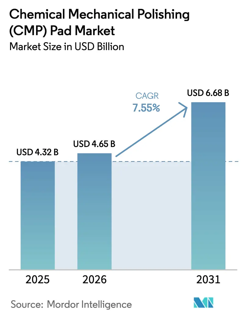
| Market Size (2026) | USD 4.65 Billion |
| Market Size (2031) | USD 6.68 Billion |
| Growth Rate (2026 - 2031) | 7.55% CAGR |
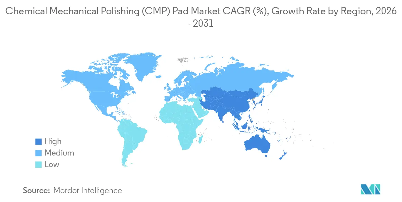
| Fastest Growing Market | Asia Pacific |
| Largest Market | Asia Pacific |
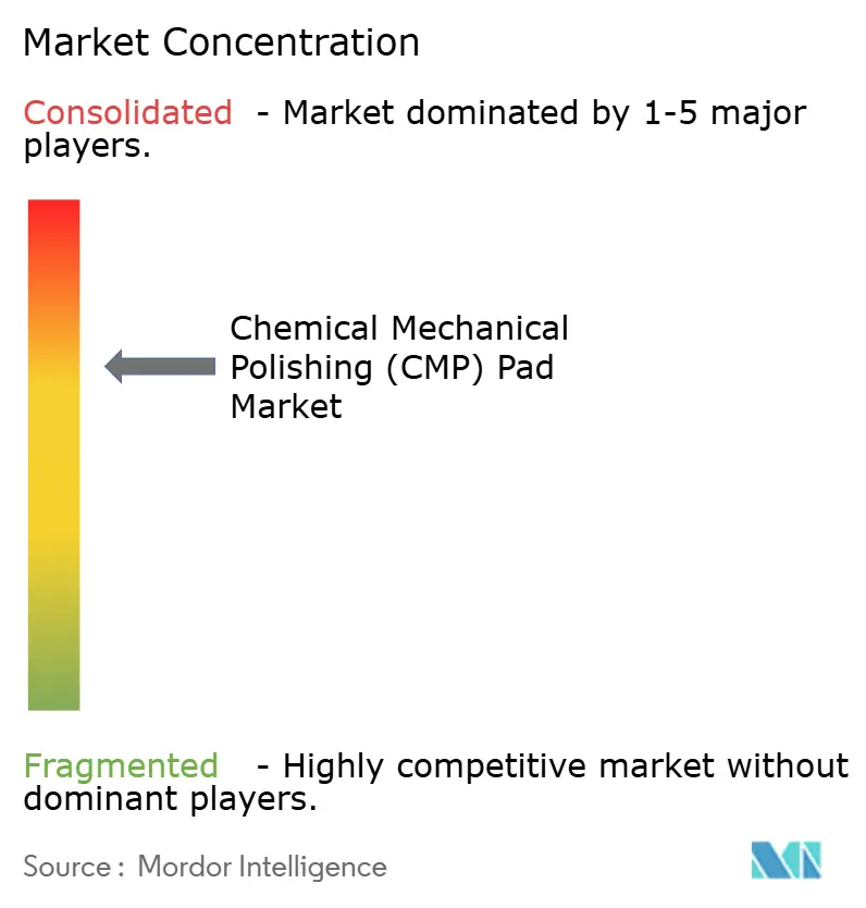
| Market Concentration | Medium |
Major Players *Disclaimer: Major Players sorted in no particular order Image © Mordor Intelligence. Reuse requires attribution under CC BY 4.0. | |
Chemical Mechanical Polishing (CMP) Pad Market Analysis by Mordor Intelligence
The Chemical Mechanical Polishing CMP Pad market size is expected to grow from USD 4.32 billion in 2025 to USD 4.65 billion in 2026 and is forecast to reach USD 6.68 billion by 2031 at 7.55% CAGR over 2026-2031. Rapid logic-device scaling, high-bandwidth memory proliferation, and the steady increase in CMP steps per extreme-ultraviolet layer all reinforce a sustained rise in pad consumption.[1]Source: Semiconductor Equipment & Materials International, “World Fab Forecast 2025,” semi.org Investments in 300 mm fabs, especially across East Asia, are bringing forward larger wafer starts that translate directly into incremental pad surface-area demand. Environmental rules that restrict per- and polyfluoroalkyl substances (PFAS) are reshaping material development priorities, and supply tightness for petro-based polyurethane is prompting producers to evaluate composite alternatives. Competitive dynamics remain rooted in performance differentiation at sub-3 nm nodes, yet cost sensitivity persists in mature processes, forcing suppliers to segment portfolios carefully.
Key Report Takeaways
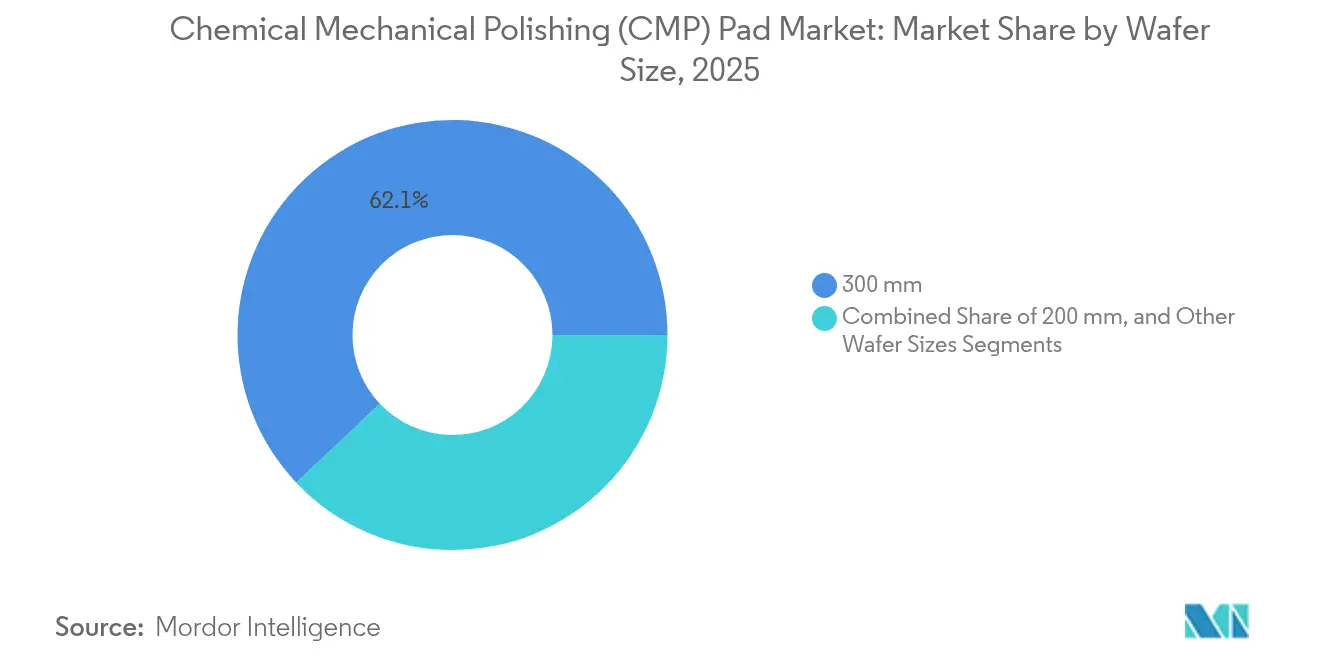
- By wafer size, 300 mm substrates held 62.05% of the Chemical Mechanical Polishing CMP Pad market share in 2025 while registering an 8.55% CAGR outlook to 2031.
- By pad material, thermoset polyurethane accounted for 54.45% of the Chemical Mechanical Polishing CMP Pad market size in 2025, whereas porous polymer composites are projected to expand at an 8.25% CAGR through 2031.
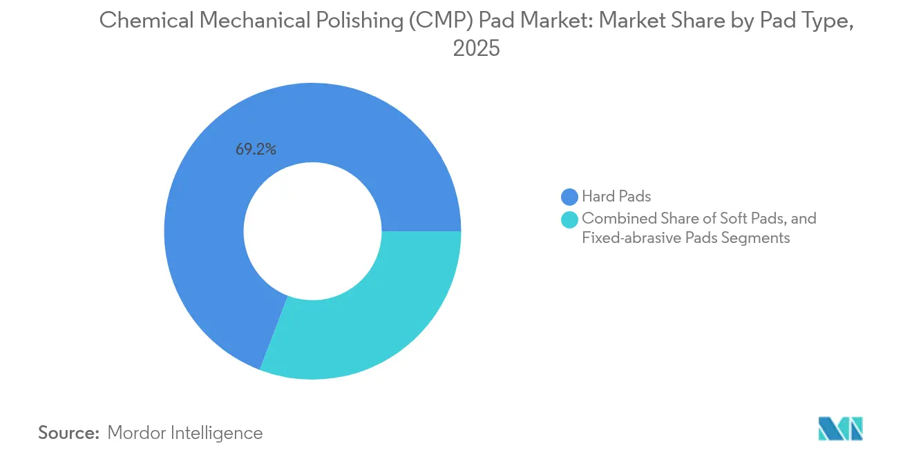
- By pad type, hard pads dominated with 69.20% revenue share in 2025; soft pads are poised for the fastest 9.10% CAGR to 2031.
- By device application, logic captured 35.25% of the Chemical Mechanical Polishing CMP Pad market size in 2025, while memory pads are expected to grow at a 8.65% CAGR toward 2031.
- By geography, Asia-Pacific commanded 39.85% of 2025 revenue and is predicted to post a 9.35% CAGR through 2031, the fastest among all regions.
Note: Market size and forecast figures in this report are generated using Mordor Intelligence’s proprietary estimation framework, updated with the latest available data and insights as of 2026.
Global Chemical Mechanical Polishing (CMP) Pad Market Trends and Insights
Drivers Impact Analysis*
| DRIVER | (~) % IMPACT ON CAGR FORECAST | GEOGRAPHIC RELEVANCE | IMPACT TIMELINE |
|---|---|---|---|
| AI-enabled design-rule shrink | +1.2% | Global: highest in Taiwan and Korea | Medium term (2-4 years) |
| Growing wafer starts at 300 mm fabs | +1.8% | Asia-Pacific core; Americas spill-over | Short term (≤ 2 years) |
| Rapid logic foundry capacity additions | +1.5% | Taiwan, Korea; emerging Germany and Arizona | Medium term (2-4 years) |
| Higher CMP steps per EUV layer | +2.1% | Advanced-node fabs worldwide | Long term (≥ 4 years) |
| Adoption of 3D-DRAM | +0.9% | Korea and China; global cross-license | Medium term (2-4 years) |
| Recycling-as-a-service programs | +0.4% | North America and Europe; Asia scaling | Long term (≥ 4 years) |
| Source: Mordor Intelligence | |||
AI-Enabled Design-Rule Shrink
Aggressive logic road-maps now target 2 nm mass production, adding as many as 15 incremental CMP passes versus prior 7 nm flows. Every successive node tightens within-wafer thickness specifications, compelling pad vendors to furnish materials with nanometer-grade surface control. Next-generation porous composites couple sub-10 nm defectivity with stable removal rates, a balance that traditional polyurethane struggles to deliver. Parallel advances in fab-wide artificial-intelligence control loops allow real-time process tuning, which in turn raises expectations that pads will sustain performance under dynamically changing pressure and speed settings. Together, these factors elevate the strategic value of high-end CMP pads across leading-edge logic lines.
Growing Wafer Starts at 300 mm Fabs
Semiconductor manufacturers have scheduled more than a dozen new 300 mm facilities for ramp between 2025 and 2027. Each 300 mm wafer presents roughly 40% more surface area than a 200 mm wafer, yet it typically runs through a greater number of CMP steps, magnifying pad consumption per device. Higher substrate value also supports premium materials that minimize defect risk, prompting fabs to qualify low-scratch, long-life pads even for mixed-node environments. Suppliers that can guarantee consistent material response across copper, tungsten, and low-k stacks gain a competitive edge inside diversified mega-fabs.
Rapid Logic Foundry Capacity Additions
Geopolitical and supply-chain resilience objectives are driving advanced logic construction in the United States, Germany, and Japan, supplementing entrenched clusters in Taiwan and Korea. Each new site requires localized technical-support infrastructure, compelling pad companies to broaden service footprints while preserving global product uniformity. At 3 nm and below, gate-all-around architectures call for entirely new mechanical compliance ranges, accelerating the need for application-specific pad chemistries. This distributed build-out opens fresh revenue pools for suppliers that can navigate cross-regional qualification protocols.
Higher CMP Steps per EUV Layer
EUV patterning replaces multi-pattern DUV schemes yet paradoxically expands CMP count because of resist-residue cleaning and pellicle interface control. Fabs report up to 25 CMP passes on a single logic device layer, intensifying pad throughput requirements well beyond wafer-start growth. As high-NA EUV enters pilot lines by 2027, depth-of-focus shrinkage will further constrain topography budgets, pushing pad performance toward atomically flat planarization. Vendors capable of aligning pad roughness profiles to resist chemistry will capture value in this high-margin niche.
Restraints Impact Analysis*
| RESTRAINT | (~) % IMPACT ON CAGR FORECAST | GEOGRAPHIC RELEVANCE | IMPACT TIMELINE |
|---|---|---|---|
| Semiconductor cap-ex cyclicality | -0.8% | Global; Asia-Pacific most exposed | Short term (≤ 2 years) |
| Escalating pad qualification timelines | -1.1% | Advanced-node fabs worldwide | Medium term (2-4 years) |
| Petro-based polyurethane supply tightness | -0.6% | North America and Europe | Short term (≤ 2 years) |
| Environmental limits on slurry waste | -0.4% | North America and Europe; Asia uptake | Long term (≥ 4 years) |
| Source: Mordor Intelligence | |||
Semiconductor Cap-Ex Cyclicality
Down-cycles typically curb equipment outlays for 12-18 months, triggering steep but temporary contractions in consumables demand. Mature-node fabs then receive a larger slice of wafers, depressing adoption of next-generation pad designs and prolonging sales cycles. Vendors with broad portfolios can mitigate shocks by reallocating inventory toward automotive or power segments, whereas niche players risk revenue gaps.
Escalating Pad Qualification Timelines
Advanced-node validation now spans 12-18 months because fabs require extensive statistical confidence across multiple integrations and sites. The elongated lead time strains vendor cash flow while raising barriers for new entrants, effectively concentrating the field among players that can underwrite long qualification programs. Suppliers counteract by engaging earlier in process-development kits to gain co-ownership of integration recipes.
*Our forecasts treat driver/restraint impacts as directional, not additive. The impact forecasts reflect baseline growth, mix effects, and variable interactions.
Segment Analysis
By Wafer Size: 300 mm Hegemony Sustains Momentum
300 mm substrates occupied 62.05% of 2025 revenue and continue to anchor capacity additions. Foundry leaders allocate most green-field investments to this diameter, reinforcing scale advantages in throughput and line yield. The Chemical Mechanical Polishing CMP Pad market size attributable to 300 mm lines is projected to increase as lithographic road-maps delay any meaningful 450 mm migration until beyond 2030; the runway for 300 mm pad shipments remains intact.
Applications such as wafer-level chip-scale packaging now loop 300 mm wafers through post-fabrication CMP steps for redistribution layer leveling, adding incremental pad demand atop front-end needs. In contrast, 200 mm lines serve legacy analog and power devices where pad performance thresholds are lower and price sensitivity is higher, cushioning revenue even through economic cycles. Niche diameters under 150 mm persist for compound semiconductors, yet their aggregate volume barely dents the mainstream pad market.


By Pad Material: Thermoset Dominance Meets Composite Surge
Thermoset polyurethane maintains core relevance thanks to proven mechanical rigidity and slurry compatibility. Nevertheless, sub-3 nm topography specifications expose their limitations in scratch suppression, catalyzing an 8.25% CAGR upswing for porous polymer composites. These engineered matrices embed controlled porosity, channeling slurry to the interface while dampening shear stress, thus reducing micro-scratches.
Thermoplastic pads, though smaller in value, address recyclability mandates and find traction where device margins or environmental credits offset their higher initial cost. Material selection is increasingly application-specific: copper interconnects demand robust stiffness, while low-k dielectric CMP favors compliant surfaces. Vendors differentiate by tailoring filler chemistry and pore structure, often co-optimizing with proprietary slurries to guarantee holistic performance.
By Pad Type: Hard Pads Reign but Soft Pads Accelerate
Hard pads supply the muscle for copper damascene, tungsten plug, and bulk backside grinding, yielding a commanding 69.20% slice of 2025 revenue. Slurry-free fixed-abrasive variants, an evolution of hard pads, integrate alumina or ceria particles directly into the matrix, lowering chemical volumes and curtailing slurry waste. Their uptake remains modest today but stands to widen as fabs pursue sustainability and tighter defect budgets.
Soft pads, indispensable for advanced packaging, rise on the coattails of hetero-integration schemes such as chiplets and wafer-to-wafer hybrid bonding. Their 9.10% CAGR through 2031 reflects new demand pathways instead of cannibalizing hard-pad volumes. Process engineers often deploy mixed pad stacks hard pad for global planarization, followed by a soft pad for final polish, to navigate diverse material layers without substrate damage, underscoring the complementary coexistence of these sub-segments.
By Device Application: Logic Leads, Memory Gains Velocity
Logic devices, notably CPUs and AI accelerators, consumed 35.25% of pad shipments in 2025, reflecting high CMP intensity at advanced interconnect levels. The Chemical Mechanical Polishing CMP Pad market size allocated to logic is anticipated to increase by 2030 as nanosheet transistors spread across foundries. Memory applications 3D-DRAM and high-layer NAND register the quickest 8.65% gauge, their vertical architectures posing unique staircase and channel CMP challenges that favor softer, high-porosity pads.
Analog and mixed-signal devices continue to rely on larger geometry nodes, yet still need CMP for back-end metallization, ensuring baseline volume stability. Specialized pads are also emerging for silicon photonics and power GaN, though these remain small profit pools until broader commercial traction materializes.
Geography Analysis
Asia-Pacific remains the epicenter of the Chemical Mechanical Polishing CMP Pad market, capturing 39.85% of 2025 turnover. Multiple 300 mm logic and memory expansions across Taiwan and South Korea underpin a regional 9.35% CAGR toward 2031. China’s domestic memory push adds further volume, although export-control headwinds temper equipment flow. Japan’s strategic subsidies for new EUV lines and its leadership in CMP slurry production provide additional tailwinds.
North America’s share benefits from U.S. CHIPS-Act incentives that bankroll advanced node facilities in Arizona, Ohio, and Texas. These fabs demand localized pad manufacturing and just-in-time logistics, creating openings for both incumbents and startups. Europe’s rising profile stems from logic and power-device investments in Germany and Italy; stringent PFAS regulations there accelerate the adoption of composite pads that meet eco-design standards.
The rest of the world contributes smaller but growing pockets. Southeast Asia leverages assembly know-how to move upstream into front-end fabrication, notably in Malaysia and Singapore, which favor integrated CMP service centers. The Middle East and Africa remain exploratory, with proposed fabs in the Gulf states still years from volume production.

Competitive Landscape
Market leadership rests with a handful of global suppliers that hold decades-deep patent portfolios and maintain in-line conditioning and slurry businesses, enabling them to deliver turnkey CMP ecosystems. DuPont’s Ikonic series exemplifies integrated architecture with performance gains across removal rate, defectivity, and pad life. Entegris emphasizes segment-specific lines for 3D-NAND and DRAM, while CMC Materials targets mid-node cost optimization.[4]Source: Entegris Inc., “2025 Investor Presentation,” entegris.com
Regional challengers in China, Taiwan, and Korea pursue rapid iteration cycles to close performance gaps, often leveraging price as an entry lever in mature nodes. Nonetheless, lengthy qualification windows and customer aversion to yield risk constrain immediate displacement of incumbents at leading-edge lines. Vertical integration trends intensify as pad vendors acquire conditioner and slurry assets to lock in synergistic revenue and simplify fab vendor lists.
Environmental, social, and governance (ESG) filters grow sharper, rewarding suppliers that can document PFAS-free chemistries and circular-economy models. Recycling pilots shift value perception from one-time consumable sale to a a lifecycle service contract, augmenting switching costs and deepening customer lock-in.
Chemical Mechanical Polishing (CMP) Pad Industry Leaders
3M Company
DuPont de Nemours Inc.
Entegris Inc.
Cabot Microelectronics (CMC Materials)
Fujibo Holdings Inc.
- *Disclaimer: Major Players sorted in no particular order

Recent Industry Developments
- March 2025: TSMC commenced construction of a second Kumamoto plant targeting 2027 output with integrated advanced packaging lines that will consume purpose-built through-silicon-via CMP pads.
- February 2025: CXMT reached steady-state 200,000 DRAM wafers per month, intensifying regional demand for memory-optimized planarization consumables.
- January 2025: Fujifilm completed a 30% capacity hike at its Kumamoto CMP-slurry facility, citing AI semiconductor demand across the Asia-Pacific.
- December 2024: SEMI projected 18 new global fabs to break ground in 2025, including 15 at the 300 mm scale, reinforcing multiyear pad volume visibility.


Global Chemical Mechanical Polishing (CMP) Pad Market Report Scope
CMP pads are integral to the semiconductor industry's CMP (chemical mechanical polishing or planarization) process, which is crucial for flattening and polishing silicon wafers. These pads, typically crafted from hard, porous polyurethane foam, feature intricate, high-aspect-ratio grooves. The study tracks the revenue generated from the sale of chemical mechanical polishing pads (CMP) offered by different market players for a diverse range of applications. The market trends are evaluated by analyzing the investments made in product innovation, diversification, and expansion. The study further analyses the aftereffects of COVID-19 and other macroeconomic factors on the market. The report's scope encompasses market sizing and forecasts for the various market segments.
The chemical mechanical polishing (CMP) pads market is segmented by wafer size (300 mm and 200 mm) and geography (North America, Europe, China, South Korea, Japan, Taiwan, and Rest of the World). The market sizes and forecasts are provided in terms of value (USD) for all the above segments.
| 300 mm |
| 200 mm |
| Other Wafer Sizes |
| Thermoset Polyurethane |
| Thermoplastic Polyurethane |
| Porous Polymer Composites |
| Hard Pads |
| Soft Pads |
| Fixed-abrasive Pads |
| Logic | |
| Memory | DRAM |
| NAND | |
| Other Memory | |
| Analog | |
| Other Device Applications |
| North America | United States | |
| Canada | ||
| Mexico | ||
| South America | Brazil | |
| Argentina | ||
| Rest of South America | ||
| Europe | Germany | |
| United Kingdom | ||
| France | ||
| Italy | ||
| Spain | ||
| Russia | ||
| Rest of Europe | ||
| Asia-Pacific | China | |
| Japan | ||
| India | ||
| South Korea | ||
| South-East Asia | ||
| Rest of Asia-Pacific | ||
| Middle East and Africa | Middle East | Saudi Arabia |
| United Arab Emirates | ||
| Rest of Middle East | ||
| Africa | South Africa | |
| Egypt | ||
| Rest of Africa | ||
| By Wafer Size | 300 mm | ||
| 200 mm | |||
| Other Wafer Sizes | |||
| By Pad Material | Thermoset Polyurethane | ||
| Thermoplastic Polyurethane | |||
| Porous Polymer Composites | |||
| By Pad Type | Hard Pads | ||
| Soft Pads | |||
| Fixed-abrasive Pads | |||
| By Device Application | Logic | ||
| Memory | DRAM | ||
| NAND | |||
| Other Memory | |||
| Analog | |||
| Other Device Applications | |||
| By Geography | North America | United States | |
| Canada | |||
| Mexico | |||
| South America | Brazil | ||
| Argentina | |||
| Rest of South America | |||
| Europe | Germany | ||
| United Kingdom | |||
| France | |||
| Italy | |||
| Spain | |||
| Russia | |||
| Rest of Europe | |||
| Asia-Pacific | China | ||
| Japan | |||
| India | |||
| South Korea | |||
| South-East Asia | |||
| Rest of Asia-Pacific | |||
| Middle East and Africa | Middle East | Saudi Arabia | |
| United Arab Emirates | |||
| Rest of Middle East | |||
| Africa | South Africa | ||
| Egypt | |||
| Rest of Africa | |||


Key Questions Answered in the Report
What is the projected value of the Chemical Mechanical Polishing CMP Pad market in 2031?
The market is expected to reach USD 6.68 billion by 2031 on the back of a 7.55% CAGR.
Which wafer size category drives the highest pad demand?
300 mm wafers account for 62.05% of 2025 revenue and are forecast to remain the dominant diameter through 2031.
Which pad material segment is growing the fastest?
Porous polymer composites are poised for an 8.25% CAGR as sub-3 nm nodes require lower defectivity.
How do environmental regulations influence pad development?
PFAS and solvent restrictions accelerate the shift toward fluorine-free materials and pad-recycling business models.
Which region offers the highest growth opportunity for pad suppliers?
Asia-Pacific shows the fastest 9.35% CAGR through 2031, fueled by large-scale logic and memory expansions.
Page last updated on:


