Thin Wafer Processing And Dicing Equipment Market Size and Share
Market Overview
| Study Period | 2020 - 2031 |
|---|---|
| Market Size (2026) | USD 0.82 Billion |
| Market Size (2031) | USD 1.11 Billion |
| Growth Rate (2026 - 2031) | 6.32% CAGR |
| Fastest Growing Market | Asia Pacific |
| Largest Market | Asia Pacific |
| Market Concentration | Medium |
Major Players
*Disclaimer: Major Players sorted in no particular order Image © Mordor Intelligence. Reuse requires attribution under CC BY 4.0. |
|
Thin Wafer Processing And Dicing Equipment Market Analysis by Mordor Intelligence
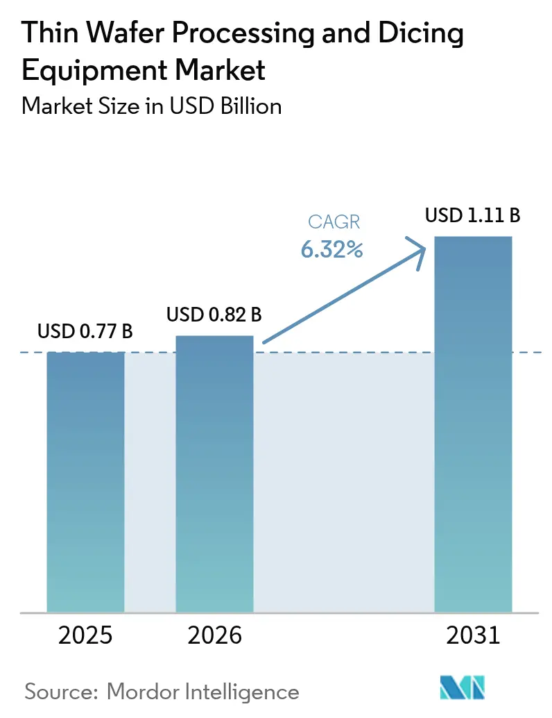
Thin Wafer Processing and Dicing Equipment market size in 2026 is estimated at USD 0.82 billion, growing from 2025 value of USD 0.77 billion with 2031 projections showing USD 1.11 billion, growing at 6.32% CAGR over 2026-2031. Accelerated demand for 3D-IC packaging, through-silicon vias, and high-performance power devices keeps precision wafer thinning and singulation tools at the center of semiconductor capital spending plans. Foundry investments in 2nm logic nodes, the rapid adoption of silicon-carbide power electronics for electric vehicles, and government-funded 3D-IC pilot lines in China and the European Union create sustained equipment demand, while process innovations such as plasma and stealth dicing widen supplier differentiation. Capital intensity and yield-critical warpage risks remain key hurdles; nonetheless, the thin wafer processing and dicing equipment market continues to benefit from structural miniaturization trends in consumer, automotive, and data-center electronics.
Key Report Takeaways
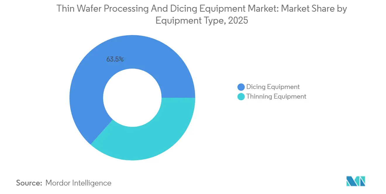
- By equipment type, dicing tools held 63.45% of the thin wafer processing and dicing equipment market share in 2025; thinning tools recorded the fastest growth rate of 7.06% from 2025 to 2031.
- By application, memory and logic TSV captured 31.80% of the thin wafer processing and dicing equipment market size in 2025, while power devices led growth at 8.16% CAGR.
- By wafer size, the 12-inch segment accounted for a 46.20% share of the thin wafer processing and dicing equipment market size in 2025 and is expected to advance at an 7.99% CAGR.
- By wafer thickness, the 120 µm segment accounted for a 39.70% share of the thin wafer processing and dicing equipment market size in 2025, while the 50 µm segment led growth at a 7.44% CAGR.
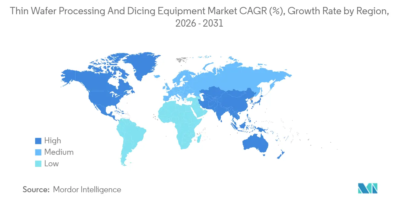
- By geography, the Asia-Pacific region accounted for a 59.65% revenue share in 2025 and is forecast to expand at an 8.05% CAGR through 2031.
Note: Market size and forecast figures in this report are generated using Mordor Intelligence’s proprietary estimation framework, updated with the latest available data and insights as of 2026.
Global Thin Wafer Processing And Dicing Equipment Market Trends and Insights
Drivers Impact Analysis*
| DRIVER | (~) % IMPACT ON CAGR FORECAST | GEOGRAPHIC RELEVANCE | IMPACT TIMELINE |
|---|---|---|---|
| Rising adoption of RFID, smart cards, and automotive power ICs | +1.2% | Global with Asia-Pacific and Europe concentration | Medium term (2-4 years) |
| Surge in 3D-IC TSV memory and logic demand | +1.8% | Asia-Pacific core, spill-over to North America | Medium term (2-4 years) |
| Ongoing miniaturization of consumer electronics | +1.5% | Global, led by Asia-Pacific hubs | Long term (≥ 4 years) |
| CAPEX race for ≥6 kW laser plasma dicing tools | +0.9% | Asia-Pacific and North America | Short term (≤ 2 years) |
| Subsidies for 3D-IC pilot lines in China and Europe | +0.7% | China and Europe | Medium term (2-4 years) |
| Rapid uptake of plasma dicing for ultra-thin SiC power devices | +0.4% | Global, with early adoption in automotive markets | Long term (≥ 4 years) |
| Source: Mordor Intelligence | |||


Rising Adoption of RFID, Smart Cards and Automotive Power ICs
Contactless payment cards and vehicle electrification require dies with thicknesses of ≤120 µm for radio-frequency efficiency and thermal performance. Silicon-carbide traction inverters in battery-electric cars rely on wafers with thicknesses below 100 µm to reduce thermal resistance, which in turn drives demand for advanced grinding, CMP, and stress-relief modules. Automotive cockpit digitalization further boosts demand for high-performance SoCs that require precise thickness control and low-stress die singulation.[1]Source: Panasonic Automotive Systems, “Panasonic Automotive Systems and Qualcomm Expand Collaboration,” news.panasonic.com As a result, OEMs specify narrower thickness tolerances and lower kerf widths, lifting average selling prices for premium thinning and plasma-dicing tools. This tailwind directly supports revenue expansion in the thin wafer processing and dicing equipment market.
Surge in 3D-IC TSV Memory and Logic Demand
Chipmakers are moving toward vertical integration to bypass the limits of planar scaling. TSV-stacked DRAM and chiplet-based CPUs require wafers to be thinned to ≤50 µm, which traditional double-side grind systems cannot process without inducing warpage. Leading foundries have earmarked multi-billion-dollar budgets for 2nm logic ramps that include large batches of carrier-de-bond, laser-debond, and plasma-dicing tools.[2]Source: “Tokyo Electron & IBM Renew Collaboration for Advanced Semiconductor Technology,” TechPowerUp, techpowerup.com The shift amplifies throughput requirements: a single 2 nm fab can consume 60,000 300 mm wafers per month, each pass obligating ultra-clean singulation to protect TSV sidewalls. Consequently, equipment suppliers offering integrated metrology and real-time stress compensation gain share inside the thin wafer processing and dicing equipment market.
Ongoing Miniaturization of Consumer Electronics
Smartphones, wearables, and hearables strive for thinner profiles while packing additional cameras, AI accelerators, and bigger batteries. Wafer thickness specifications have tightened from ±5 µm a decade ago to ±2 µm for premium handset SoCs, prompting adoption of multi-step grind-polish processes that combine diamond wheels with slurry-free CMP. Leading handset OEMs align with foundry roadmaps at 3nm nodes that mandate advanced die-stack packaging, further intensifying the adoption of stealth and plasma dicing. Height-restricted microphones, pressure sensors, and camera image sensors also need ultra-precise edge integrity to secure assembly yields, channeling more capital toward high-accuracy singulation systems and reinforcing momentum for the thin wafer processing and dicing equipment market.
CAPEX Race Among Foundries for ≥6 kW Laser Plasma Dicing Tools
Competition among tier-one foundries centers on yield improvement at nodes below 5 nm. High-power laser plasma systems deliver sub-3 µm kerf widths, reduce die chipping, and enhance edge strength, making them indispensable for brittle compound semiconductors, such as gallium nitride. A single ≥6 kW dicer carries a price tag in excess of USD 5 million, yet operators justify the outlay through double-digit die-per-wafer gains and lower clean-room contamination. Partnership announcements such as the five-year technology extension between Tokyo Electron and IBM underscore the appetite for collaborative research and development in laser-based singulation. Early adopters secure competitive cycle-time advantages, thereby sustaining the premium segment within the Thin wafer processing and dicing equipment market.
Restraints Impact Analysis*
| RESTRAINT | (~) % IMPACT ON CAGR FORECAST | GEOGRAPHIC RELEVANCE | IMPACT TIMELINE |
|---|---|---|---|
| Wafer warpage and die-cracking yield losses | -1.1% | Global, node-advanced fabs | Short term (≤ 2 years) |
| High upfront cost of advanced thinning/dicing lines | -0.8% | Global, heavier on small fabs | Medium term (2-4 years) |
| Shortage of epi-ready ultra-thin SiC/GaN wafers | -0.6% | Global, concentrated in power device applications | Long term (≥ 4 years) |
| Tightening environmental rules on laser ablation particulates | -0.3% | Europe and North America, spreading to Asia-Pacific | Medium term (2-4 years) |
| Source: Mordor Intelligence | |||
Wafer Warpage and Die-Cracking Yield Losses
Reducing wafer thickness below 100 µm magnifies internal stress gradients and accentuates post-grind bow, often exceeding ±80 µm on a 300 mm substrate. Bow-corrective carriers and chuck-level active compensation add cost and complexity yet remain essential, as yield losses from die cracking can reach 10-15% in aggressive TSV stacks. Plasma-based singulation introduces localized heating, which can worsen warp if chuck cooling is inadequate, necessitating closed-loop thermal management. Until defect-density metrics match those of 200 µm historical baselines, adoption curves for advanced thinning lines may progress in staged rollouts, dampening near-term revenue potential for the thin wafer processing and dicing equipment market.
High Upfront Cost of Advanced Thinning/Dicing Lines
A complete line integrating grind, CMP, temporary bond-debond, stealth or plasma dicing, and inline metrology can exceed USD 50 million, a threshold unattainable for many specialty IDMs. Tier-two fabs often outsource to service providers, thereby relinquishing control over their schedules. Even large incumbents demonstrate capex selectivity: DISCO has earmarked USD 275 million for capacity expansion to maintain its edge in high-accuracy dicing.[3]Source: Jen-Chieh Chiang & Jingyue Hsiao, “DISCO invests JPY 40 billion in new plant,” DIGITIMES Asia, digitimes.com Financing challenges lengthen sales cycles and concentrate power among vendors able to bundle tools, service, and leasing packages, constraining the addressable customer pool within the thin wafer processing and dicing equipment market.
*Our forecasts treat driver/restraint impacts as directional, not additive. The impact forecasts reflect baseline growth, mix effects, and variable interactions.
Segment Analysis
By Equipment Type: Dicing Dominance Faces Thinning Challenge
Dicing platforms captured 63.45% of the thin wafer processing and dicing equipment market share in 2025, reflecting the indispensable demand for die-singulation across both legacy and leading-edge nodes. Conventional blade systems still dominate high-volume consumer ICs, thanks to mature cost-per-cut metrics; however, plasma and stealth variants are registering double-digit yearly bookings as customers shift to wafer-level packages that cannot tolerate blade-induced microcracks. Thinning tools are expected to record a 7.06% CAGR, outpacing general equipment growth and signaling an architectural pivot toward sub-50 µm stacks. Integrated metrology, vibration-free stages, and AI-driven thickness feedback loops collectively raise ASPs, so the thinning segment already commands a greater revenue-per-unit ratio inside the thin wafer processing and dicing equipment market.
Market penetration parallels process-node divergence. Wafers targeted for advanced 3D integration often undergo back-grinding to a thickness of ≤50 µm, followed by plasma dicing, a process that practically doubles the tool demand per wafer compared to traditional blade lines. Conversely, mature logic and analog fabs defer capex unless product performance mandates ultra-thin handling. Suppliers leverage modular chassis designs to retrofit legacy lines, shortening payback periods and expanding their total accessible Thin wafer processing and dicing equipment market size. In parallel, new entrants specializing in vacuum-less plasma chambers are courting compound semiconductor makers, nibbling away at the share of incumbents reliant on blade technology and driving competitive turnover.


By Application: Power Devices Accelerate Past Memory Leadership
Memory and logic TSV processes held 31.80% of the thin wafer processing and dicing equipment market size in 2025 due to the immediate 3D-stacking benefits within HBM modules used in AI server accelerators. Yet power semiconductors post the fastest 8.16% CAGR, fueled by traction inverters, onboard chargers, and renewables-linked power conversion that depend on wide-bandgap devices. These materials require ultra-clean kerf edges and present higher hardness, aligning perfectly with plasma and stealth dicing value propositions. As electric-vehicle unit shipments increase, tool demand intensifies far beyond proportional wafer counts, because SiC substrates typically break more blades and must transition to laser or plasma singulation early.
The power segment’s capital appetite reshuffles growth share inside the thin wafer processing and dicing equipment market. Automotive OEM qualification regimes require multi-site redundancy, thereby increasing the number of equipment installations. Meanwhile, MEMS and RFID continue to experience mid-single-digit expansion, offering steady recurring parts sales for consumable-driven blade systems. CMOS image sensors are thriving in multi-camera smartphones and autonomous-driving ADAS systems; however, many CIS fabs are migrating to 200 mm lines, tempering unit value relative to 300 mm TSV logic. Suppliers that can span these divergent requirements with unified control software improve stickiness, supporting lifetime revenue per customer.
By Wafer Thickness: Ultra-Thin Segments Drive Innovation
The 120 µm bracket accounted for 39.70% of the thin wafer processing and dicing equipment market share in 2025, as it strikes a balance between manageable handling and respectable package height reduction. Going forward, the 50 µm class is expected to exhibit the strongest growth, with a 7.44% CAGR, driven by vertical-stacked DRAM and chiplet interposers. Transitioning from 120 µm to 50 µm demands carrier-bonding hardware, low-stress chemical polish, and warp-sensing analytics, each incrementally increasing per-wafer tool consumption and broadening the thin wafer processing and dicing equipment market size. Below 50 µm, total solutions remain scarce, indicating ripe opportunity for innovation.
Processing below 100 µm can lead to non-linear warpage escalation on 300 mm silicon. Equipment OEMs now offer dual-temperature chuck plates and active backside gas pressure cushions to mitigate bow. Such complexity drives ASP escalation, yet customers accept premiums given the die-per-wafer uplift and heterogeneous integration benefits. As applications converge on wafer-level fan-out plus TSV interposers, market consensus targets final thicknesses of 20-40 µm within five years, sustaining a technology pull that cements ultra-thin processing as the innovation frontier of the thin wafer processing and dicing equipment market.

By Wafer Size: 12-Inch Dominance Accelerates
At 46.20% revenue, 300 mm substrates dominate capital allocation and are projected to grow at an 7.99% CAGR through 2031. Advanced logic, HBM, and leading-edge CIS all reside on 12-inch lines, requiring high-throughput grinders, CMP, temporary bond-debond, and plasma dicers sized for the larger diameter. Tool builders focus research and development on robotic arms with tighter planarity specs and higher blanket-vacuum uniformity to prevent deflection on expanded surface areas. The 8-inch segment serves analog, power-discrete, and niche MEMS fabrication and grows more slowly yet remains profitable because tooling for smaller diameters enjoys depreciated, high-margin consumables.
Attempts to advance 450 mm pilot lines remain on hold, channeling all next-generation node demand into 300 mm flows, which intensifies unit volume for a single size and compounds economies of scale in the thin wafer processing and dicing equipment market. Compound-semiconductor wafer diameters lag due to boule-growth constraints, so multi-format fabs need to persist, encouraging suppliers to maintain configurable platforms that handle 150 mm to 300 mm hardware on unified software. Growth concentration in 12-inch formats, however, tilts research and development budgets, guaranteeing that next-level process features first appear on the larger format before trickling down.
Geography Analysis
Asia-Pacific’s 59.65% share in 2025 stems from Taiwan’s foundry leadership, South Korea’s memory output, and China’s subsidy-backed capacity buildout. The region’s 8.05% CAGR benefits from a wave of fab announcements, including plans for four 2nm facilities coming online by 2026, which alone call for 60,000 300mm wafers per month and intensive thin-wafer processing. Japanese equipment makers, such as DISCO and Tokyo Seimitsu, supply a majority of blade and stealth dicing systems, ensuring regional vendor proximity and after-sales service density that reinforce Asia-Pacific dominance in the thin wafer processing and dicing equipment market.
North America ranks second as U.S. industrial policy stimulates domestic production. Foundry expansions linked to CHIPS Act incentives require parity with Asian process performance, including the importation of advanced CMP, carrier-bond, and plasma-dicing technologies. Large capital commitments by multinational IDMs shorten payback periods for equipment vendors and diversify geographic revenue streams. Environmental, health, and safety regulations push fabs to adopt low-particulate plasma tools over blade systems, modestly nudging technical mixes sold into the North American Thin wafer processing and dicing equipment market.
Europe’s semiconductor strategy skews toward automotive and industrial devices. Investments target silicon-carbide power fabs and advanced packaging pilot lines supported by the European Chips Act. Strict emissions guidelines within the European Union are accelerating the retirement of wet-chemistry thinning paths in favor of closed-loop, abrasive-less CMP and dry laser ablation systems, thereby fostering a premium niche for environmentally optimized tools. Although Europe’s absolute wafer volume trails that of the Asia-Pacific and North America, its high-specification procurement profile lifts the average revenue per tool, sustaining its contribution to the global thin wafer processing and dicing equipment market.

Competitive Landscape
The thin wafer processing and dicing equipment industry shows moderate concentration led by DISCO Corporation, Tokyo Seimitsu, and others. Proprietary kerf control, vibration isolation, and real-time thickness calibration underpin their market advantage, prompting continuous plant expansions such as DISCO’s USD 275 million capacity upgrade in 2024. Applied Materials leverages synergies between deposition and CMP to cross-sell grind-polish modules bundled with metrology, while laser specialists introduce plasma chambers with self-cleaning electrodes to target compound semiconductor customers.
Technology rivalry centers on plasma versus stealth dicing. Plasma systems tout contamination-free edges and minimal chipping on ultra-hard SiC substrates; stealth dicing offers sub-3 µm kerf without the need for narrow street widths. Ecosystem partnerships have intensified: Tokyo Electron has renewed its five-year development pact with IBM to co-engineer next-generation laser debond flows that reduce the total cost of ownership on carrier-bonded wafers.[4]Source: “Tokyo Electron & IBM Renew Collaboration for Advanced Semiconductor Technology,” TechPowerUp, techpowerup.com Vendors also integrate AI software that predicts bow during grind sequences, augmenting yield-impact mitigation and serving as a non-hardware revenue stream within the Thin wafer processing and dicing equipment market.
Emerging competitors exploit white-space niches, such as GaN power HEMTs and photonics ICs, where wafer materials differ markedly from those of bulk silicon. Niche players offer compact plasma dicing systems tailored for 150 mm lines serving photonics prototypes, thereby bypassing the cost barrier associated with full-scale 300 mm platforms. Consolidation pressures are mounting, especially in China, where authorities aim to merge over 200 domestic tool suppliers into 10 larger groups to gain scale and reduce import dependence. Implementation challenges persist, yet the policy signals ongoing capital support that injects new players into future bidding rounds.
Thin Wafer Processing And Dicing Equipment Industry Leaders
-
Disco Corporation
-
Tokyo Seimitsu Co., Ltd. (ACCRETECH)
-
Applied Materials, Inc.
-
Han’s Laser Technology Industry Group Co., Ltd.
-
Plasma-Therm LLC
- *Disclaimer: Major Players sorted in no particular order


Recent Industry Developments
- September 2025: Panasonic Industry allocated JPY 17 billion (USD 115 million) for a new Thai plant producing multilayer circuit-board materials for AI server modules.
- April 2025: Tokyo Electron and IBM have renewed a five-year research and development alliance to enhance laser debonding and plasma dicing technologies for sub-2 nm nodes.
- April 2025: China has accelerated plans to consolidate approximately 200 domestic chip-tool firms into 10 groups to strengthen its indigenous equipment capacity.
- February 2025: 3M joined the US-JOINT Consortium to co-develop next-generation advanced packaging materials at a new Silicon Valley research and development hub.


Global Thin Wafer Processing And Dicing Equipment Market Report Scope
| Thinning Equipment | |
| Dicing Equipment | Blade Dicing |
| Laser Ablation | |
| Stealth Dicing | |
| Plasma Dicing |
| Memory and Logic (TSV) |
| MEMS Devices |
| Power Devices |
| CMOS Image Sensors |
| RFID |
| Others |
| 750 µm |
| 120 µm |
| 50 µm |
| <4 inch |
| 5-6 inch |
| 8 inch |
| 12 inch |
| North America | United States | |
| Canada | ||
| Mexico | ||
| South America | Brazil | |
| Argentina | ||
| Rest of South America | ||
| Europe | Germany | |
| United Kingdom | ||
| France | ||
| Russia | ||
| Rest of Europe | ||
| Asia-Pacific | China | |
| Japan | ||
| India | ||
| South Korea | ||
| South-East Asia | ||
| Rest of Asia-Pacific | ||
| Middle East and Africa | Middle East | Saudi Arabia |
| United Arab Emirates | ||
| Rest of Middle East | ||
| Africa | South Africa | |
| Egypt | ||
| Rest of Africa | ||
| By Equipment Type | Thinning Equipment | ||
| Dicing Equipment | Blade Dicing | ||
| Laser Ablation | |||
| Stealth Dicing | |||
| Plasma Dicing | |||
| By Application | Memory and Logic (TSV) | ||
| MEMS Devices | |||
| Power Devices | |||
| CMOS Image Sensors | |||
| RFID | |||
| Others | |||
| By Wafer Thickness | 750 µm | ||
| 120 µm | |||
| 50 µm | |||
| By Wafer Size | <4 inch | ||
| 5-6 inch | |||
| 8 inch | |||
| 12 inch | |||
| By Geography | North America | United States | |
| Canada | |||
| Mexico | |||
| South America | Brazil | ||
| Argentina | |||
| Rest of South America | |||
| Europe | Germany | ||
| United Kingdom | |||
| France | |||
| Russia | |||
| Rest of Europe | |||
| Asia-Pacific | China | ||
| Japan | |||
| India | |||
| South Korea | |||
| South-East Asia | |||
| Rest of Asia-Pacific | |||
| Middle East and Africa | Middle East | Saudi Arabia | |
| United Arab Emirates | |||
| Rest of Middle East | |||
| Africa | South Africa | ||
| Egypt | |||
| Rest of Africa | |||


Key Questions Answered in the Report
What is the current value of the thin-wafer processing equipment space?
The thin wafer processing and dicing equipment market size stands at USD 0.82 billion in 2026 and is projected to hit USD 1.11 billion by 2031.
Which tool class dominates capital spending?
Dicing systems hold 63.45% revenue share, though thinning platforms are growing faster at a 7.06% CAGR.
Why is plasma dicing gaining momentum?
Plasma dicing delivers cleaner kerf edges and lower mechanical stress, benefits that are critical for fragile ultra-thin wafers used in 3D-IC and wide-bandgap power devices.
Which region buys the most thin-wafer tools?
Asia-Pacific controls 59.65% of global demand, supported by dense foundry clusters in Taiwan, South Korea, China, and Japan.
How do wafer-thickness trends affect equipment demand?
Movement from 120 µm toward 50 µm wafers increases process steps and drives uptake of advanced grind-polish and carrier-debond solutions.
What restrains wider adoption of ultra-thin processing?
Yield losses from wafer warpage and the high upfront cost of full thin-wafer lines remain the primary barriers.
Page last updated on:


