Automated Optical Inspection Equipment Market Size and Share
Market Overview
| Study Period | 2020 - 2031 |
|---|---|
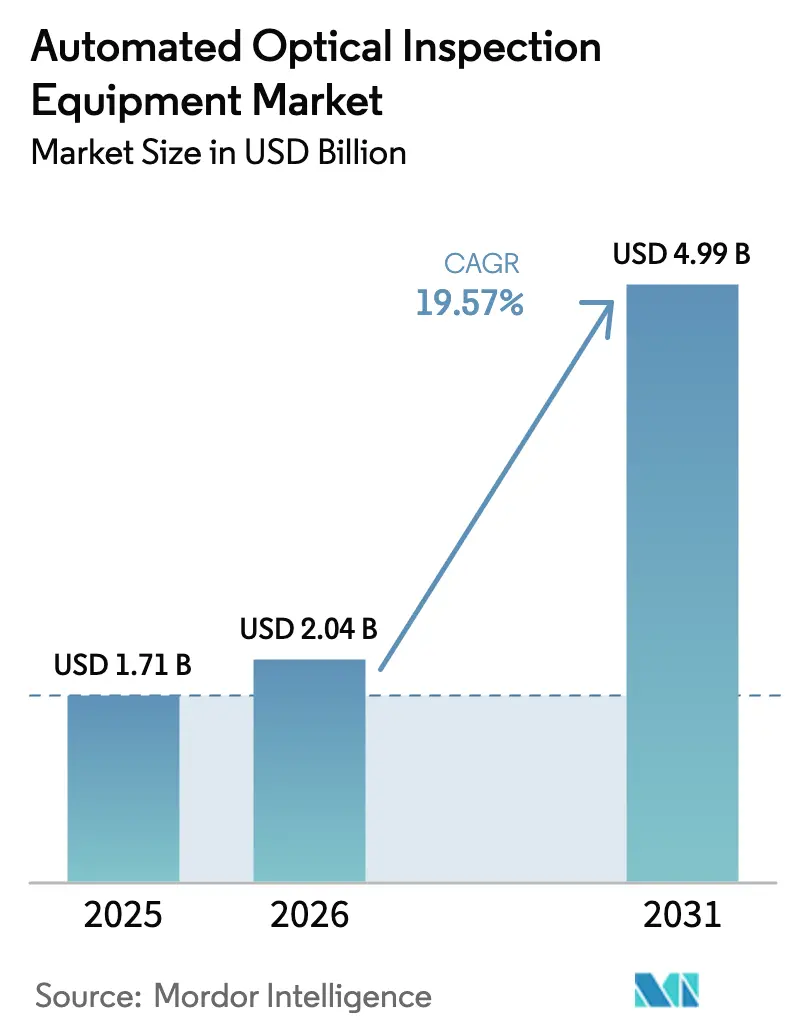
| Market Size (2026) | USD 2.04 Billion |
| Market Size (2031) | USD 4.99 Billion |
| Growth Rate (2026 - 2031) | 19.57% CAGR |
| Fastest Growing Market | Middle East and Africa |
| Largest Market | Asia Pacific |
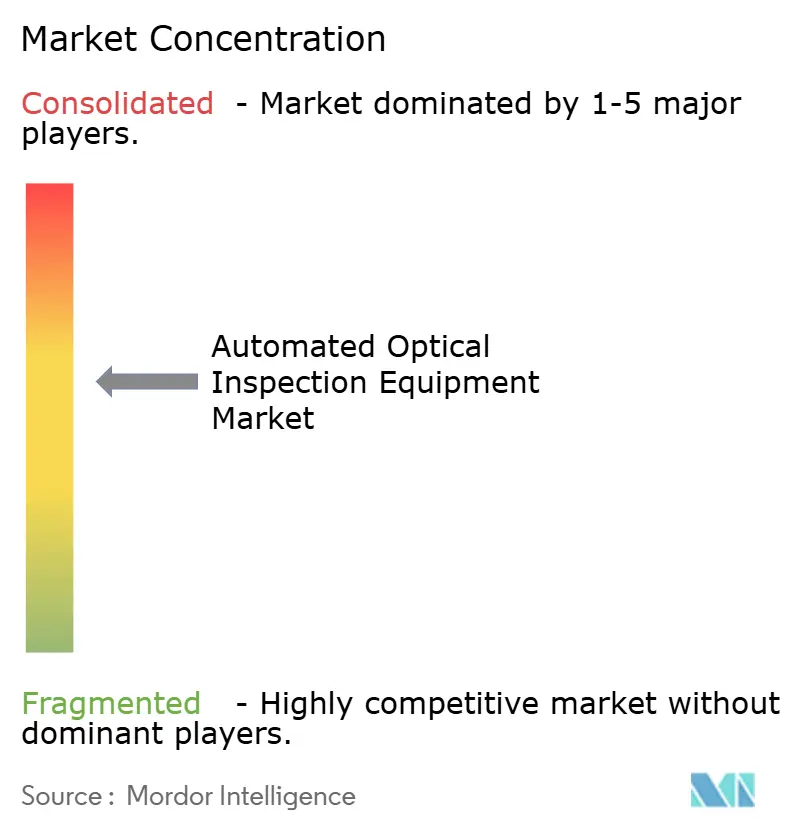
| Market Concentration | Medium |
Major Players*Disclaimer: Major Players sorted in no particular order Image © Mordor Intelligence. Reuse requires attribution under CC BY 4.0. | |
Automated Optical Inspection Equipment Market Analysis by Mordor Intelligence
The automated optical inspection equipment market size was valued at USD 1.71 billion in 2025 and estimated to grow from USD 2.04 billion in 2026 to reach USD 4.99 billion by 2031, at a CAGR of 19.57% during the forecast period (2026-2031). The automated optical inspection equipment market size for 2025 reflects the electronics sector’s move from 2D inspection toward true 3D metrology that can resolve sub-10 µm features demanded by chiplet packaging lines.[1]SEMI, “Global Total Semiconductor Equipment Sales Forecast to Reach a Record of $139 Billion in 2026,” semi.org Inline systems integrated with edge computing are lowering false-call rates and enabling closed-loop process control, which boosts first-pass yields at high-volume PCB plants in Asia and North America. Reshoring investments supported by the CHIPS Act and comparable European incentives have redirected a portion of AOI demand toward new fabs and EMS lines under construction in Ohio, New York and Saxony. Suppliers are also capitalizing on accelerated automotive electrification, where battery-management PCBs require zero-escape inspection standards to secure ISO 26262 functional-safety compliance. Persistent component shortages and trade-compliance reviews for high-speed cameras nevertheless keep lead-times volatile, pushing integrators to favor modular platforms that can be upgraded when restrictions ease.
Key Report Takeaways
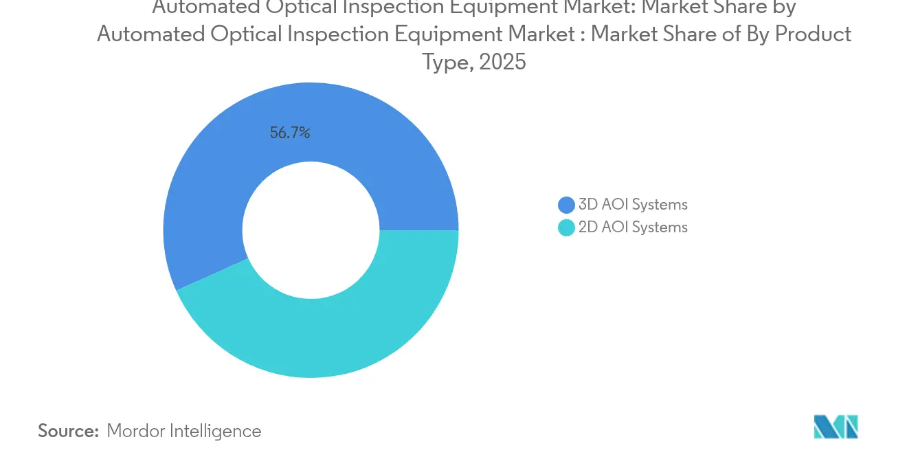
- By product type, 3D systems held 56.72% of the automated optical inspection equipment market share in 2025; 3D solutions are projected to expand at a 13.86% CAGR through 2031.
- By technology, inline installations dominated with 62.75% revenue share in 2025, while offline/desktop units are forecast to post the fastest 12.06% CAGR to 2031.
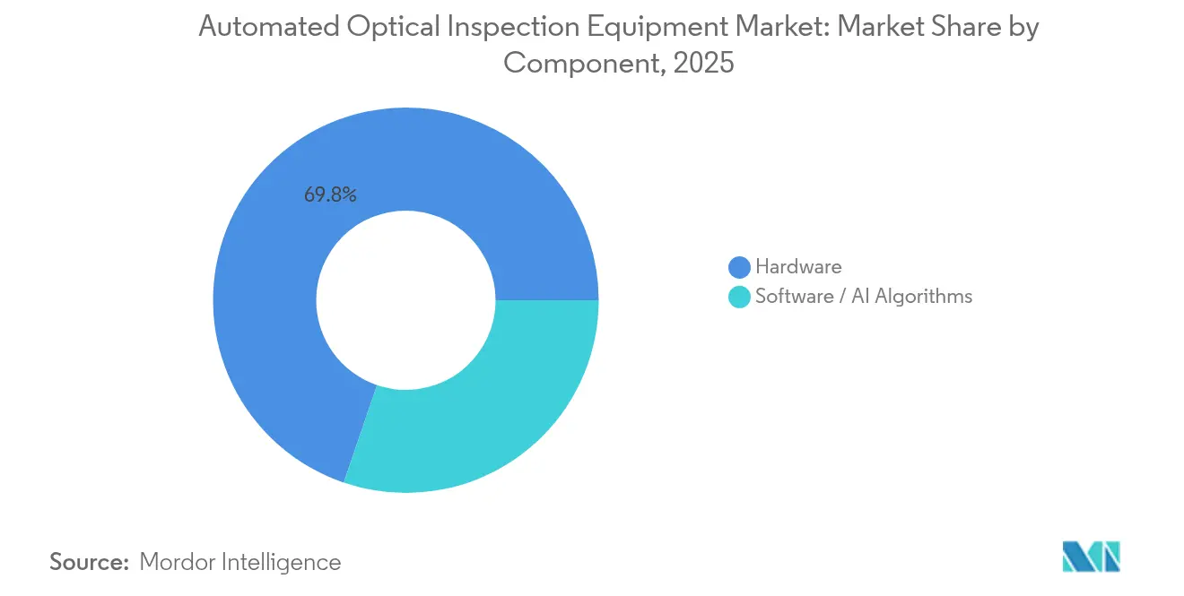
- By component, hardware accounted for 69.78% of automated optical inspection equipment market size in 2025, whereas software and AI algorithms will grow at a 15.93% CAGR between 2026-2031.
- By end-use industry, PCB and EMS providers led with 41.85% revenue share in 2025; advanced packaging lines are expected to register the highest 19.58% CAGR during the outlook period.
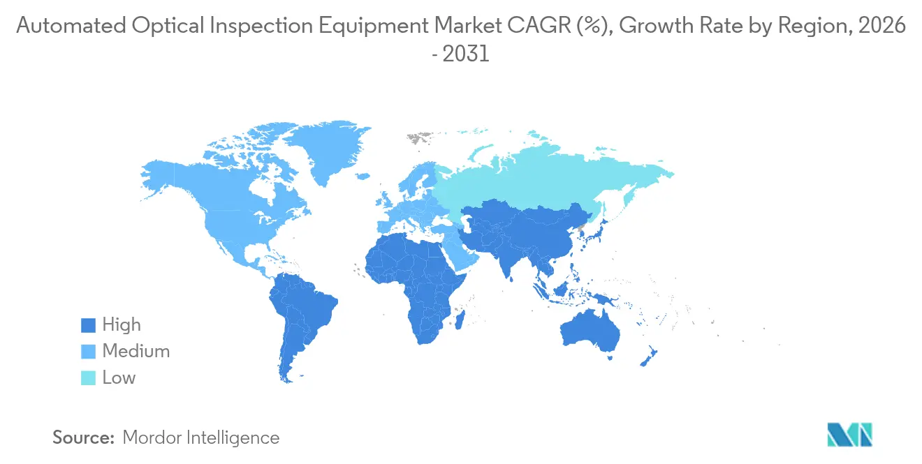
- By geography, Asia-Pacific commanded 56.65% of 2025 revenue, but the Middle East and Africa region is on track for a 13.92% CAGR to 2031.
Note: Market size and forecast figures in this report are generated using Mordor Intelligence’s proprietary estimation framework, updated with the latest available data and insights as of 2026.
Global Automated Optical Inspection Equipment Market Trends and Insights
Drivers Impact Analysis*
| Driver | (~) % Impact on CAGR Forecast | Geographic Relevance | Impact Timeline |
|---|---|---|---|
| Increasing demand for high-density, miniaturized PCBs | +3.2% | Global, with concentration in Asia-Pacific and North America | Medium term (2-4 years) |
| Transition from 2D to true-3D inspection capability | +4.1% | Global, led by advanced manufacturing regions | Medium term (2-4 years) |
| Rapid adoption of AI-enabled adaptive learning algorithms | +2.8% | North America and EU leading, APAC following | Short term (≤ 2 years) |
| Electronics manufacturing reshoring in North America and Europe | +2.5% | North America and EU primary, spill-over to Mexico | Long term (≥ 4 years) |
| Edge-computing AOI for real-time process correction | +1.9% | Advanced manufacturing hubs globally | Medium term (2-4 years) |
| Growth of chiplet and advanced-packaging lines needing sub-10 µm inspection | +3.7% | APAC core, expanding to North America | Long term (≥ 4 years) |
| Source: Mordor Intelligence | |||
Increasing Demand for High-Density, Miniaturized PCBs
Component footprints shrank from 0402 to 0201 packages and are now moving toward 01005, forcing inspection resolutions below 10 µm while production takt times remain unchanged. TRI’s TR7700Q SII platform demonstrated 1 µm resolution by deploying synchronized multi-camera 3D imaging for zero-escape inspection of power-train PCBs. Automakers adopted such capability to protect battery-management assemblies, as evidenced by Tesla’s qualification of next-generation AOI on its safety-critical control boards. Medical-implant makers likewise mandated sub-10 µm coverage to secure product approvals, and 5G radio boards now require void-free solder volumes to assure mmWave signal integrity. These converging needs are accelerating replacement of legacy 2D stations with high-precision 3D platforms across both tier-one and tier-two EMS sites.
Transition from 2D to True-3D Inspection Capability
Legacy 2D systems cannot quantify coplanarity or solder-ball volume under BGAs and chip-scale packages, which leads to latent defects in field service. Omron’s VT-S1080 adopted Multi-Direction Multi-Color illumination to reduce setup time by 70% while raising volumetric accuracy to semiconductor-grade thresholds. KLA extended the concept to advanced packaging, channeling a portion of its USD 3.08 billion Q2 FY 2025 revenue into 3D metrology R&D that addresses chiplet bridges and through-silicon via voids. Inline 3D feedback now triggers automatic stencil cleaning or solder-paste deposition correction, which increases first-pass yield and minimizes downstream X-ray verification. The market therefore continues to migrate toward 3D AOI as board densities climb.
Rapid Adoption of AI-Enabled Adaptive Learning Algorithms
False-call ratios that once hovered near 50% for complex boards have fallen below 4% on lines retrofitted with AI classifiers trained on tens of thousands of defect images. Koh Young embedded adaptive models that self-tune thresholding in real time, shortening new-product introduction by days and freeing skilled technicians for higher-value tasks. Cogiscan reported manual verification time savings reaching 60%, which relieves staffing shortages that EMS plants experienced amid tight labor markets. Some AOI suppliers now bundle edge servers that host inference engines locally, eliminating cloud latency and safeguarding confidential design data. As algorithm libraries grow, detection escapes continue to decline, reinforcing the return on software licensing over pure hardware upgrades.
Electronics Manufacturing Reshoring in North America and Europe
The United States allocated USD 50 billion under the CHIPS Act, while Intel committed USD 20 billion for a fab campus in Ohio and Micron started a 2.4 million ft² memory plant in New York, each requiring end-to-end inline inspection. Similar dynamics appeared in Europe, where more than half of UK producers surveyed in 2024 planned to repatriate assembly to counter supply chain disruptions. This redistribution has turned formerly export-focused AOI vendors into local-service providers, spurring investments in regional demo centers and spare-parts hubs. Because labor rates are higher at onshore sites, managers prioritize AI-driven AOI to offset costs through yield gains and reduced manual re-inspection.
Restraints Impact Analysis*
| Restraint | (~) % Impact on CAGR Forecast | Geographic Relevance | Impact Timeline |
|---|---|---|---|
| High CAPEX and integration complexity of inline 3D AOI | -2.1% | Global, particularly affecting SMEs | Short term (≤ 2 years) |
| Short product lifecycles demanding frequent re-programming | -1.8% | Consumer electronics hubs in APAC | Medium term (2-4 years) |
| Limited availability of AOI-talent for AI data-labelling | -1.5% | North America and EU primarily | Long term (≥ 4 years) |
| Trade-compliance barriers on imaging sensors and lasers | -1.2% | US-China trade corridors | Medium term (2-4 years) |
| Source: Mordor Intelligence | |||
High CAPEX and Integration Complexity of Inline 3D AOI
An inline 3D station costs USD 500,000–2 million per lane and demands precision conveyors, environmental isolation and MES interfacing. IPC surveys showed 90% of board houses contended with input-cost spikes averaging 14.5% as semiconductor shortages lingered, leaving limited headroom for capital purchases. Small EMS shops therefore postpone upgrades and rely on offline deskside units that cannot keep pace with high-mix high-volume lines, perpetuating a two-tier adoption pattern. Integration also requires trained technicians and spare parts, bringing total cost of ownership above initial quotations, which can delay ROI beyond three years for low-volume manufacturers.
Trade-Compliance Barriers on Imaging Sensors and Lasers
The US Bureau of Industry and Security expanded export-control codes in 2024 to cover high-speed cameras capable of 13.43 gigapixels per second and laser modules used in wafer metrology. Chinese countermeasures added license reviews for gallium-based optoelectronic components, leading to longer procurement cycles. AOI builders that embed such parts must now file license applications or redesign optics, often incurring 6-12 month delays and up to 10% extra development cost. Smaller vendors lacking dedicated compliance teams risk shipment holds that erode competitiveness and push customers toward larger firms with global logistics capacity.
*Our forecasts treat driver/restraint impacts as directional, not additive. The impact forecasts reflect baseline growth, mix effects, and variable interactions.
Segment Analysis
By Product Type: 3D Systems Extend Metrology Frontiers
3D platforms generated 56.72% of 2025 revenue, reflecting the automated optical inspection equipment market’s pivot to volumetric measurement at line speeds. That share rose as semiconductor and automotive clients demanded co-planarity verification and paste-height analytics unavailable on 2D gear. The automated optical inspection equipment market size attributed to 3D systems is projected to climb at 13.86% CAGR through 2031, propelled by shrinking pad pitches in chiplet assemblies. 2D variants remain relevant for consumer electronics where surface-level scratch and polarity checks suffice, especially in contract factories pursuing extreme throughput.
The cost gap between 2D and 3D is narrowing as sensor prices fall and algorithm libraries mature. Fraunhofer’s SURFinpro prototype proved that AI can reconstruct solder geometries with fewer cameras, trimming bill-of-material cost while approaching 3D accuracy. As a result, late-adopter EMS firms see improved ROI, which accelerates the retirement of legacy 2D lines. Because process analytics now tie paste-volume readings to stencil-cleaning cycles, operators gain actionable data that curtails scrap and warranty returns.


By Technology: Inline Dominance Mirrors Industry 4.0 Adoption
Inline machines secured 62.75% share in 2025 by providing closed-loop feedback that quarantines defects before downstream assembly. Inline shipments within the automated optical inspection equipment market are forecast to advance at 11.74% CAGR as Industry 4.0 pilots transition to plant-wide rollouts. Edge servers housed inside the inspection frame let models run locally so that paste-print offsets trigger printer adjustments without operator intervention.
Offline/desktop units continue to serve low-volume medical or aerospace boards requiring extended dwell time under high-magnification optics. These systems saw renewed interest among small businesses deterred by inline CAPEX. Yet the inline advantage has grown as enterprise MES suites now ingest AOI images to predict stencil wear and derive Cpk indicators that auditors accept. Consequently, line designers specify inline AOI as standard for new surface-mount tracks across North America, Europe and progressive APAC factories.
By Component: Hardware Backbone Enables Software Upside
Hardware captured 69.78% of 2025 revenue, comprising cameras, telecentric lenses and strobed lighting arrays tailored for 01005 inspection. Nonetheless, software and AI modules are projected to grow 15.93% annually, reshaping vendor business models toward subscription updates. Applied Materials’ Vera platform illustrates the shift: deep-UV lasers married to convolutional-neural-network classifiers expose sub-µm contamination that once required e-beam sampling.
Component makers are integrating higher-dynamic-range sensors to supply training datasets with fewer frame drops, raising detection accuracy on shiny solder domes. Meanwhile, algorithm vendors monetize continuous-improvement packs that lower false-calls every quarter, locking customers into multi-year service contracts. The convergence yields composite offerings in which hardware revenue subsidizes AI roadmaps, almost doubling lifetime customer value compared with one-off capital sales.
By End-Use Industry: Semiconductor Lines Drive Out-Sized Growth
PCB and EMS operators preserved 41.85% of 2025 turnover due to sheer production volume, yet semiconductor fabs and advanced-packaging subcontractors are projected to clock a 19.58% CAGR, the fastest among verticals. Their need for sub-10 µm coverage across wafer-level redistribution layers magnifies spending per line, lifting the automated optical inspection equipment market share of this segment as heterogenous integration ramps.
Automotive electrification, medical implants and mmWave radios contribute incremental demand, but the wafer-centric user base is more willing to pay premium pricing for early access releases with enhanced optics. Qorvo’s deployment of high-throughput AOI on GaN wafers exemplified how defect-density analytics now inform epi-wafer tuning and plasma etch parameters, extending tool utility beyond final inspection. Solar-cell strings and EV battery tabs have also become fertile niches, as manufacturers seek AI-driven AOI to minimize micro-cracks that degrade conversion efficiency.
Geography Analysis
Asia-Pacific retained 56.65% of 2025 revenue on the strength of China’s USD 49 billion semiconductor-equipment outlays and Taiwan’s panel-level packaging projects led by TSMC. The automated optical inspection equipment market size attributed to Asia-Pacific remains substantial, yet policy risk and rising wages spurred some OEMs to diversify into Vietnam, India and Malaysia, dispersing new AOI orders across the region. Japan’s mature automotive electronics base continued investing in 3D metrology lines that validate heat-sink coplanarity for SiC inverter boards.
North America’s share expanded as CHIPS Act grants and local procurement policies drove fabs to source inline inspection domestically. Capital spending on US equipment is projected to reach USD 24.7 billion in 2027, ensuring steady AOI backlog, although an estimated 80,000 unfilled technician posts could constrain throughput if workforce.. Mexico captured spill-over EMS contracts under USMCA, prompting AOI vendors to open service centers in Nuevo León to support near-shoring lines.
Europe pursued technological self-reliance, channeling climate-policy funds toward energy-efficient AOI modules that cut power draw by 20%. Germany’s Tier-1 auto suppliers ordered line-scan 3D units for silicon-carbide power modules, while Nordic start-ups adopted AI-based AOI for battery-cell tabs in gigafactories. Supply-chain complexity following Brexit added customs paperwork, but localized inventory pools in the Netherlands trimmed lead-times for EU customers.
Middle East and Africa, though still small, recorded the fastest 13.92% CAGR outlook as governments under industrial-diversification agendas lured PCB assemblers and LED lighting producers with tax incentives. Saudi Arabia’s electronic-manufacturing corridor near Riyadh placed initial orders for entry-level inline AOI capable of 0201 inspection, signaling future upgrades to 3D as skill levels rise.

Competitive Landscape
Industry concentration is moderate, with top five suppliers accounting for roughly 45% of 2024 revenue. KLA, Omron, Koh Young, and Viscom each leverage long-term service contracts and AI feature roadmaps to retain customers, while emergent software specialists target brown-field retrofits. KLA’s USD 3.06 billion Q3 FY 2025 revenue and USD 5 billion share-buyback authorization underscore the cash reserves incumbents deploy for M&A and R&D.
AI-centric challengers such as Averroes.ai demonstrated 97% detection accuracy on mixed-technology boards, slashing false positives to 4% and courting EMS houses reluctant to replace functional hardware.[3]Silicon Semiconductor, “Beyond AOI: An AI-Driven Revolution in Visual Inspection,” siliconsemiconductor.net Hardware players responded by embedding edge processors and licensing third-party neural networks to protect installed bases. Partnerships that blend operational-technology know-how with IT consulting, exemplified by Omron and Cognizant, signal a pivot toward holistic factory-digital-twin offerings that raise switching costs.
Patent filings on AOI image-classification techniques surpassed 200 in 2024, reflecting a race to secure algorithmic IP that differentiates subtle defect-type identification. Vendors with deep optics portfolios invest in tailor-made illumination, while software-only entrants rely on transfer-learning to adapt models across camera types. Talent scarcity in machine-vision engineering remains a bottleneck; firms are poaching university graduates with equity grants and remote-work options to accelerate model-training pipelines.
Automated Optical Inspection Equipment Industry Leaders
KLA Corporation
Applied Materials, Inc.
ASML Holding N.V.
Hitachi High-Tech Corporation
Lam Research Corporation
- *Disclaimer: Major Players sorted in no particular order

Recent Industry Developments
- June 2025: Global Brands Manufacture acquired Japan’s Lincstech to expand AI server capability and strengthen presence in Singapore and Malaysia
- June 2025: Maister Engineering Group purchased 100% of Kanamex shares to enlarge its engineering federation amid semiconductor talent shortages
- June 2025: Lightwave Logic and Polariton Technologies extended cooperation to deliver 400 Gb/s per lane optical links for AI data centers, with a roadmap to 800 Gb/s
- May 2025: Applied Optoelectronics posted USD 99.9 million Q1 2025 revenue, doubling year over year on CATV and AI data-center demand


Global Automated Optical Inspection Equipment Market Report Scope
The Automated Optical Inspection (AOI) equipment market encompasses systems designed to inspect electronic components, assemblies, and printed circuit boards (PCBs) for defects using advanced imaging and optical technologies. These systems are widely used in electronics manufacturing to ensure quality, accuracy, and compliance with industry standards. The market includes various AOI solutions tailored for different applications, such as surface mount technology (SMT), through-hole technology (THT), and semiconductor inspection.
The Automated Optical Inspection (AOI) Equipment Market is segmented by type (2D AOI systems, 3D AOI systems), technology (inline, offline), end-use industry (semiconductor manufacturing, consumer electronics, automotive electronics, PCB manufacturing, solar panel manufacturing, medical devices, and other end-use industries), and geography (North America, Europe, Asia Pacific, Latin America, and Middle East and Africa). The market sizes and forecasts are provided in terms of value (USD) for all the above segments.
| 2D AOI Systems |
| 3D AOI Systems |
| Inline Systems |
| Offline / Desktop Systems |
| Hardware (Cameras, Illumination, Controllers) |
| Software / AI Algorithms |
| Semiconductor Manufacturing |
| PCB and EMS Providers |
| Consumer Electronics Assembly |
| Automotive Electronics |
| Solar and Battery Manufacturing |
| Medical Devices |
| Aerospace and Defense Electronics |
| North America | United States | |
| Canada | ||
| Mexico | ||
| South America | Brazil | |
| Argentina | ||
| Rest of South America | ||
| Europe | Germany | |
| United Kingdom | ||
| France | ||
| Italy | ||
| Russia | ||
| Rest of Europe | ||
| Asia-Pacific | China | |
| Japan | ||
| South Korea | ||
| India | ||
| ASEAN | ||
| Rest of Asia-Pacific | ||
| Middle East and Africa | Middle East | Saudi Arabia |
| United Arab Emirates | ||
| Turkey | ||
| Rest of Middle East | ||
| Africa | South Africa | |
| Nigeria | ||
| Rest of Africa | ||
| By Product Type | 2D AOI Systems | ||
| 3D AOI Systems | |||
| By Technology | Inline Systems | ||
| Offline / Desktop Systems | |||
| By Component | Hardware (Cameras, Illumination, Controllers) | ||
| Software / AI Algorithms | |||
| By End-use Industry | Semiconductor Manufacturing | ||
| PCB and EMS Providers | |||
| Consumer Electronics Assembly | |||
| Automotive Electronics | |||
| Solar and Battery Manufacturing | |||
| Medical Devices | |||
| Aerospace and Defense Electronics | |||
| By Geography | North America | United States | |
| Canada | |||
| Mexico | |||
| South America | Brazil | ||
| Argentina | |||
| Rest of South America | |||
| Europe | Germany | ||
| United Kingdom | |||
| France | |||
| Italy | |||
| Russia | |||
| Rest of Europe | |||
| Asia-Pacific | China | ||
| Japan | |||
| South Korea | |||
| India | |||
| ASEAN | |||
| Rest of Asia-Pacific | |||
| Middle East and Africa | Middle East | Saudi Arabia | |
| United Arab Emirates | |||
| Turkey | |||
| Rest of Middle East | |||
| Africa | South Africa | ||
| Nigeria | |||
| Rest of Africa | |||


Key Questions Answered in the Report
What is the current size of the automated optical inspection equipment market?
The automated optical inspection equipment market size reached USD 2.04 billion in 2026 and is projected to grow to USD 4.99 billion by 2031.
Why are 3D AOI systems gaining share so quickly?
3D platforms quantify solder-joint volume and coplanarity, capabilities required for chiplet packaging and sub-10 µm PCB layouts that 2D tools cannot measure accurately.
How are AI algorithms improving AOI performance?
AI classifiers have cut false positives from almost 50% to below 4% on complex boards by learning from large defect libraries and auto-tuning inspection thresholds in real time.
Which region will be the fastest-growing AOI market through 2031?
The Middle East and Africa is expected to post a 13.92% CAGR as governments invest in electronics manufacturing to diversify their economies.
What is the main hurdle for small manufacturers adopting inline 3D AOI?
Up-front capital costs ranging from USD 500,000 to USD 2 million per system, plus integration complexity with existing lines, create high entry barriers for SMEs.
Page last updated on:


