Atomic Layer Deposition Market Size and Share
Market Overview
| Study Period | 2020 - 2031 |
|---|---|
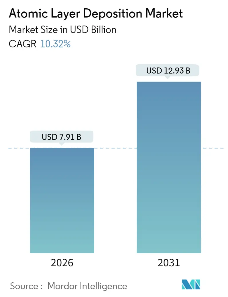
| Market Size (2026) | USD 7.91 Billion |
| Market Size (2031) | USD 12.93 Billion |
| Growth Rate (2026 - 2031) | 10.32% CAGR |
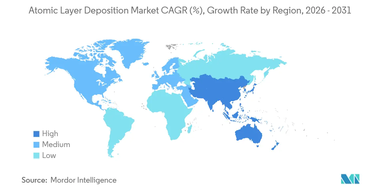
| Fastest Growing Market | Asia Pacific |
| Largest Market | Asia Pacific |
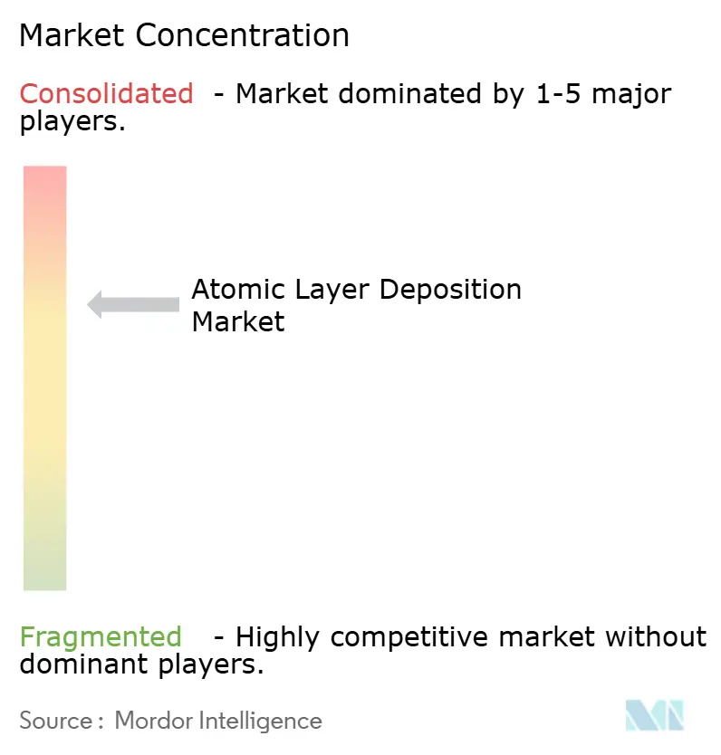
| Market Concentration | Medium |
Major Players
*Disclaimer: Major Players sorted in no particular order Image © Mordor Intelligence. Reuse requires attribution under CC BY 4.0. |
|
Atomic Layer Deposition Market Analysis by Mordor Intelligence
The atomic layer deposition market size reached USD 7.91 billion in 2026 and is projected to climb to USD 12.93 billion by 2031, reflecting a 10.32% CAGR over the forecast horizon. Rapid node migration in logic and memory, the search for higher energy densities in batteries, and demand for ultra-thin encapsulation in emerging display formats are broadening the customer base beyond mainstream semiconductor fabs. Gate-all-around transistors at 2 nanometers, 300-plus-layer 3D NAND stacks, and roll-to-roll micro-LED production all need angstrom-level thickness control that chemical vapor deposition cannot achieve, placing plasma and spatial ALD squarely in the front-end tool set. Equipment suppliers are responding with single-wafer cluster tools that isolate contamination while improving precursor utilization, and with spatial architectures that trade some precision for speed, especially in display and battery lines. Government subsidies under the United States CHIPS and Science Act and the European Union Chips Act are redirecting a portion of capital spending toward North America and Europe, yet Asia-Pacific still dominates installations thanks to entrenched capacity and local tool makers. Meanwhile, throughput gaps, precursor-metal shortages, and tightening environmental rules on fluorinated plasmas temper the growth outlook and motivate process innovations.
Key Report Takeaways
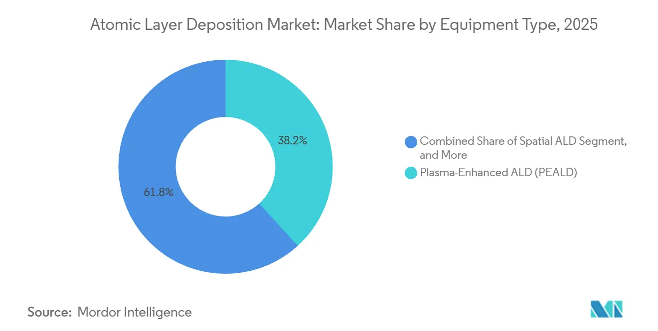
- By equipment type, plasma-enhanced systems led with 38.23% revenue share in 2025 while spatial tools are on track for a 12.41% CAGR through 2031.
- By reactor configuration, cluster single-wafer platforms accounted for 44.57% of the atomic layer deposition market share in 2025 and are expanding at an 11.02% CAGR to 2031.
- By substrate size, the 300 millimeter segment captured 57.32% of the atomic layer deposition market size in 2025 and is projected to maintain leadership even as 450 millimeter pilot lines post a 12.48% CAGR.
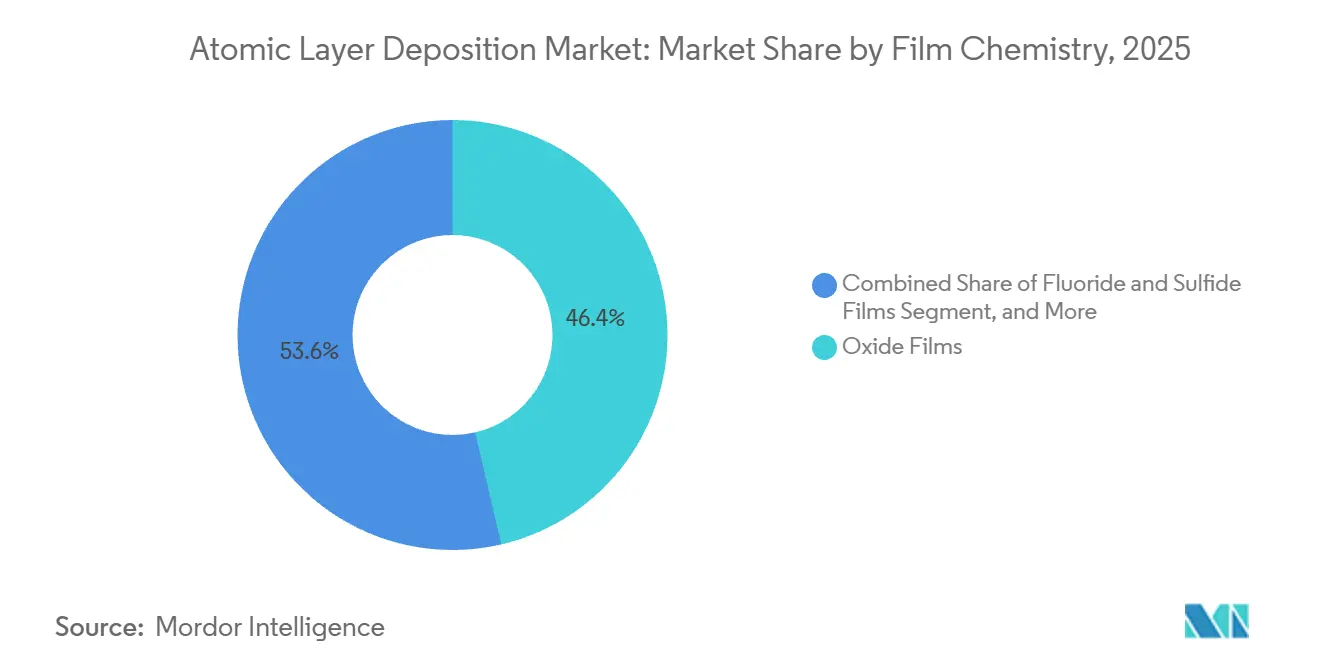
- By film chemistry, oxide coatings held 46.36% revenue share in 2025, whereas fluoride and sulfide films are recording the fastest 13.03% CAGR through 2031.
- By application, semiconductor logic and memory remained the anchor with 34.11% of 2025 revenue, yet energy-device coatings are advancing at a 12.24% CAGR on solid-state battery demand.
- By geography, Asia-Pacific commanded 53.43% revenue in 2025 and is expected to rise at an 11.28% CAGR thanks to wafer-fab expansions in Taiwan, South Korea, and China.
Note: Market size and forecast figures in this report are generated using Mordor Intelligence’s proprietary estimation framework, updated with the latest available data and insights as of January 2026.
Global Atomic Layer Deposition Market Trends and Insights
Drivers Impact Analysis*
| Driver | (~) % Impact on CAGR Forecast | Geographic Relevance | Impact Timeline |
|---|---|---|---|
| Surging 3D NAND and DRAM node shrink in Asia | +2.1% | Asia-Pacific core, spillover to North America | Medium term (2-4 years) |
| Transition to gate-all-around and high-k metal gate logic | +1.8% | Global, concentrated in Taiwan, South Korea, United States | Short term (≤ 2 years) |
| Rapid adoption of mini/micro-LED backplanes | +1.3% | Asia-Pacific manufacturing, North America design | Medium term (2-4 years) |
| EV battery solid-state electrolyte coatings demand | +1.5% | Global, early leadership in Japan, South Korea, China | Long term (≥ 4 years) |
| Medical implant nano-coatings for improved biocompatibility | +0.9% | North America and Europe regulatory markets | Long term (≥ 4 years) |
| Government-funded pilot-line investments, EU Chips Act, CHIPS and Science Act | +1.6% | North America and Europe, strategic autonomy focus | Medium term (2-4 years) |
| Source: Mordor Intelligence | |||
Surging 3D NAND And DRAM Node Shrink In Asia
Layer counts in vertical NAND exceeded 300 in 2025, forcing memory fabs to introduce up to 14 ALD steps per wafer to maintain sidewall conformality at aspect ratios above 80:1.[1]IEEE Staff, “3D NAND Scaling and ALD Integration,” IEEE Electron Device Letters, ieee.org DRAM makers also moved to 1-beta structures with capacitor diameters under 18 nanometers, a geometry that only ALD zirconium-doped hafnium oxide can fill without leakage. Samsung disclosed that ALD tools consumed 22% of memory-fab capex in 2025, up from 16% three years earlier. China’s YMTC followed suit by adding ALD titanium-nitride liners in its Xtacking 4.0 design, spending an extra USD 120 million per 100 000-wafer-per-month line. These investments reinforce Asia-Pacific’s leadership and elevate tool-demand visibility for at least the next two node shrinks.
Transition To Gate-All-Around And High-k Metal Gate Logic
Gate-all-around field-effect transistors wrap the channel with a conformal high-k dielectric, lowering equivalent oxide thickness below 0.7 nanometers. TSMC’s N2 risk-production flow calls for a 12-cycle hafnium-oxide ALD stack followed by titanium-nitride work-function metal, all deposited in isolated ALD chambers to curb oxygen cross-talk.[2]TSMC Technology Symposium, “N2 Process Technology Overview,” tsmc.com Intel’s 18A node adds a selective ALD cobalt liner that cuts contact resistance 19%. Samsung’s second-generation 3 nanometer flow achieved 23% power gains with a thinner interfacial layer credited to optimized ALD chemistry. Although ALD cycle times can top 180 seconds, foundries are mitigating bottlenecks through parallel chamber counts, underscoring the indispensable role of ALD in sub-3-nanometer logic.
Rapid Adoption Of Mini and Micro-LED Backplanes
Pixel pitches below 50 micrometers expose active layers to oxygen and moisture, making sub-10-nanometer barrier films essential. Spatial ALD meets the speed requirement by decoupling precursor exposure from purge steps, achieving linear web speeds of 10 meters per minute. LG Display ordered six spatial reactors for its Paju P10 fab in 2025, a USD 85 million commitment aimed at automotive micro-LED panels. Beneq likewise booked an eight-tool order worth EUR 65 million (USD 71 million) from an Asian display integrator. While precursor waste and recipe re-qualification slow adoption, the throughput upside continues to attract display makers.
EV Battery Solid-State Electrolyte Coatings Demand
Solid-state lithium-metal cells offer over 500 Wh/kg, yet dendrite formation limits cycle life. Five-to-20-nanometer ALD interlayers of lithium phosphorus oxynitride or aluminum oxide have extended cycle life beyond 1 000 cycles by creating robust artificial solid-electrolyte interfaces. QuantumScape reported a 34% cut in interfacial resistance with its proprietary ALD coating, enabling 0.5C charge rates without plating. Toyota’s pilot line in Aichi Prefecture is deploying eight ALD reactors to coat sulfide electrolytes for 2027 hybrid models. Although processing adds USD 12-18 per kWh, premium vehicle programs accept the trade-off, and spatial ALD promises cost relief once scale is achieved.
Restraints Impact Analysis*
| Restraint | (~) % Impact on CAGR Forecast | Geographic Relevance | Impact Timeline |
|---|---|---|---|
| Scarcity and cost volatility of precursor metals, Ru, Ir, Co | -1.4% | Global, acute in regions with limited strategic reserves | Short term (≤ 2 years) |
| Throughput limitations vs high-volume foundry targets | -1.1% | Global, most severe in Asia-Pacific high-volume fabs | Medium term (2-4 years) |
| Competing spatial CVD for OLED encapsulation | -0.7% | Asia-Pacific display manufacturing | Short term (≤ 2 years) |
| Stringent EHS regulations on fluorinated plasma by-products | -0.8% | North America and Europe, regulatory-driven markets | Long term (≥ 4 years) |
| Source: Mordor Intelligence | |||
Scarcity And Cost Volatility Of Precursor Metals
Ruthenium, iridium, and cobalt are mined mainly as platinum-group by-products in South Africa and Russia, exposing supply to geopolitical risk. Ruthenium rose from USD 450 per troy ounce in 2024 to USD 603 by end-2025 as both ALD and electrolyzer builders chased limited output. Foundries squeezed usage through smarter pulse timing, but wafer starts keep rising, so demand outpaces efficiency gains. Substitute chemistries are in trial, yet qualification cycles last two to three years, prolonging exposure to volatile spot prices.
Throughput Limitations Versus High-Volume Foundry Targets
Single-wafer plasma ALD tops out at roughly 50 wafers per hour for 10 nanometer stacks, far below the 200-wafer cadence of adjacent lithography tools. Lam’s SABRE 3D hit 160 wafers per hour for hafnium oxide but drops to 85 for cobalt due to slow nucleation. Spatial reactors promise <30 second cycles yet struggle to keep uniformity under 2% on 300 millimeter wafers. The gap inflates capital intensity as fabs buy more chambers, creating cost pressure that could curb adoption if not resolved before the 1.4 nanometer node ramps.
*Our forecasts treat driver/restraint impacts as directional, not additive. The impact forecasts reflect baseline growth, mix effects, and variable interactions.
Segment Analysis
By Equipment Type: Plasma Precision Leads While Spatial Platforms Pursue Speed
Plasma-enhanced tools generated 38.23% of 2025 revenue, a testament to their low-temperature capability that shields interconnects and compound semiconductors. The atomic layer deposition market size for plasma systems is set to rise at nearly the overall 10% CAGR through 2031 as nanosheet logic and 3D DRAM mandate sub-300 °C processing. Conformal nitride and titanium films, unachievable by thermal ALD at reasonable rates, anchor demand. In contrast, spatial architectures will post a 12.41% CAGR by trading atomic-level accuracy for linear speed, especially on flexible substrates. The WCS 500 platform coats 10 m² webs hourly, allowing display lines to meet takt-time goals previously impossible with batch chambers, though precursor waste remains 40% higher. Thermal batch tools linger in academia and biomedical lines where plasma damage is prohibitive, but their share shrinks each year as fabs consolidate around cluster designs.
Looking ahead, hybrid stacks combining plasma ALD and atomic-layer etching inside one chassis are gaining traction. Tokyo Electron’s Tactras tool reduces wafer handoffs and lifts overall productivity 18% compared with discrete modules. Suppliers that master such integration will capture incremental wallet share as fabs chase both precision and throughput. Meanwhile, battery and display producers are pushing vendors for roll-to-roll designs that equal batch uniformity at half the cost, hinting at divergent product roadmaps inside the atomic layer deposition market.


By Reactor Configuration: Cluster Flexibility Commands The Premium
Cluster single-wafer platforms delivered 44.57% of 2025 revenue and should sustain an 11.02% CAGR as logic fabs pay for contamination isolation. Each wafer occupies its own chamber, allowing rapid chemistry changes without cross-talk, critical when alternating cobalt liners with dielectric stacks. The atomic layer deposition market share for batch reactors is sliding because their lower cost per wafer cannot offset limited recipe agility at sub-7 nanometer nodes. Still, trailing-edge fabs in China procured batch tools for 38% of 2025 adds, illustrating that capital efficiency remains a deciding factor outside cutting-edge logic.
Spatial single-wafer systems blur the historical split by combining contamination control with higher mechanical throughput. If film-uniformity hurdles are solved, they could erode the premium now enjoyed by cluster tools. Suppliers are therefore hedging bets: ASM International’s Pulsar line maintains single-wafer leadership, while its new spatial portfolio targets display and battery users. Over the decade, buyer choice will hinge on whether tool makers can harmonize cycle time, film quality, and cost of ownership inside one modular frame.
By Substrate Size: 300 mm Dominance Persists As 450 mm Pilots Gather Pace
Intel’s Arizona Fab 52 will insert a 450 millimeter ALD module during its 2026 start-up, validating mechanical handling and uniformity metrics.
Power, analog, and wide-band-gap devices remain anchored at 200 millimeter or smaller formats. Gallium-nitride and silicon-carbide fabs prefer 150 millimeter substrates until defect densities fall, and Veeco’s Propel HB shows the business case for targeted 200 millimeter tools at USD 2.8 million per chamber. The result is a bifurcated supply chain, with separate optimization paths for high-volume CMOS and for specialty devices serving electric vehicles and renewable grids.
By Film Chemistry: Oxides Still Rule, Fluorides And Sulfides Accelerate
Oxides generated 46.36% of chemistry revenue in 2025, anchored by hafnium oxide gate dielectrics and aluminum oxide passivation layers. Mature precursors, predictable nucleation, and broad application scopes keep this family at the center of most process flows. Yet fluoride and sulfide films will outgrow all other categories, posting a 13.03% CAGR through 2031. Solid-state batteries employ lithium thiophosphate and lithium phosphorus oxynitride coatings to push ionic conductivity above 10 mS/cm, and Samsung SDI confirmed 41% lower interfacial resistance after adding an ALD fluoride stabilizer. Fluoride-doped hafnium zirconium oxide also lifts polarization endurance in ferroelectric memories, extending write cycles past 10¹⁰.
Metals such as cobalt and ruthenium enjoy technology-node pull but face price headwinds. Nitride growth is moderating as 3D NAND architectures approach mechanical limits on stress per stack. Consequently, precursor suppliers able to deliver high-purity fluorides and sulfides at scale stand to capture emerging value pools inside the atomic layer deposition market.
By Application: Semiconductor Anchor Funds Expansion Into Energy And Bio
Semiconductor logic and memory contributed 34.11% of 2025 revenue and will stay vital since they bankroll R&D that spills into adjacent sectors. Advanced packaging techniques, including hybrid bonding in TSMC’s System-on-Wafer platform, require ALD copper-barrier liners to stop electromigration. In parallel, energy-device coatings are climbing at a 12.24% CAGR. Nickel-rich cathodes protected by 3-nanometer ALD alumina reached over 3 000 cycles, unlocking higher-voltage packs. Biomedical coatings, though small in dollars, command premium pricing; ISO 13485 certification of Oxford Instruments’ OpAL system proves medical implant makers value ALD’s ability to enhance osseointegration without roughening surfaces.
Outside core electronics, lidar optics, infrared cameras, and automotive sensors are adopting ALD anti-reflection layers, broadening the market’s resilience against semiconductor cycles. This demand diversity underpins long-term growth even if leading-edge logic capex fluctuates year to year.
Geography Analysis
Asia-Pacific retained 53.43% revenue share in 2025 and is forecast to rise at an 11.28% CAGR through 2031. Taiwan, South Korea, and China jointly held 78% of 300 millimeter capacity, while tool makers Tokyo Electron and Hitachi High-Tech provide an indigenous supply chain that accelerates regional adoption.[3]SEMI, "World Fab Forecast," semi.org South Korea’s 3D NAND leadership drives word-line barrier and charge-trap layer demand, and China’s wafer-fab build-out absorbs equipment for mature nodes, image sensors, and power management integrated circuits. Japan benefits from equipment exports and early roll-outs of solid-state battery lines. India’s USD 10 billion semiconductor incentive has yet to translate into high-volume fabs but signals potential longer-term demand.
North America ranked second, propelled by USD 39 billion in CHIPS Act subsidies and over USD 200 billion in announced fab investments from Intel, TSMC, Samsung, and Micron. ALD tools account for about 14% of total wafer-fab equipment budgets across these projects. Canada’s role is largely research-oriented, while Mexico focuses on advanced packaging lines using ALD for copper diffusion barriers.
Europe follows on the strength of the EUR 43 billion (USD 47 billion) EU Chips Act that aims for 20% global semiconductor share by 2030. Intel’s Magdeburg fab and TSMC’s Dresden plant will deploy volume ALD modules after 2026. STMicroelectronics expands in Crolles to supply automotive customers with ALD-protected silicon-carbide devices. The Middle East and Africa remain nascent, limited to exploratory projects by investment funds.
South America’s participation is confined to academic labs; industrial capex centers on assembly rather than front-end fabrication. Consequently, the atomic layer deposition market remains highly concentrated, with the top five countries Taiwan, South Korea, China, the United States, and Japan capturing 84% of 2025 equipment revenue. Subsidies may shift the mix at the margin, yet entrenched know-how, supplier ecosystems, and existing depreciation schedules ensure Asia-Pacific’s primacy for the foreseeable future.
Mordor Intelligence provides coverage of the atomic layer deposition market across other key regional markets, including North America, each with their regulatory frameworks and demand patterns.

Competitive Landscape
Four incumbents (Applied Materials, ASM International, Tokyo Electron, and Lam Research) collectively held about 72% revenue share in 2025, reflecting scale advantages in R&D, service networks, and precursor partnerships.
Challengers such as Forge Nano, Beneq, and ALD NanoSolutions carve out niches in batteries, biomedical, and flexible electronics where established platforms lack precursor flexibility or roll-to-roll form factors. Forge Nano’s Prometheus unit coats 10 kg/h of cathode particles, an unmatched throughput for particulate ALD. Oxford Instruments is patenting cryogenic ALD for organic interfaces, and Veeco addresses 200 millimeter power devices with cost-optimized chambers.
Competitive intensity is rising because wafer-fab equipment spending dipped 8% year-over-year in 2026 amid memory oversupply. Suppliers diversify into energy storage, displays, and medical devices to smooth revenue. Technology leadership remains the winning lever; tools that deliver 20% faster cycles or 30% lower cost of ownership capture share, while legacy designs risk margin compression. Partnerships with precursor makers, in-chamber metrology, and software-defined process control are emerging differentiators as customers demand higher uptime and tighter specs.
Atomic Layer Deposition Industry Leaders
-
ASM International N.V.
-
Tokyo Electron Limited
-
Applied Materials Inc.
-
Lam Research Corporation
-
Beneq Oy
- *Disclaimer: Major Players sorted in no particular order

Recent Industry Developments
- December 2025: Applied Materials announced a USD 450 million expansion of its Bundang ALD R and D center in South Korea, adding 12 cleanroom bays targeted at gate-all-around and 3D DRAM process development.
- November 2025: ASM International acquired a spatial ALD patent portfolio from Fraunhofer for EUR 38 million (USD 41 million) to accelerate tool commercialization for flexible displays.
- October 2025: Tokyo Electron introduced the Tactras ALE-ALD cluster platform, integrating etch and deposition to boost throughput 18% for nanosheet logic nodes.
- September 2025: Lam Research formed a USD 320 million joint venture with Naura Technology Group to localize ALD and ALE tool production for China’s domestic market.


Research Methodology Framework and Report Scope
Market Definitions and Key Coverage
Our study defines the atomic layer deposition (ALD) equipment market as revenue generated from the sale of brand-new, factory-built tools that create ultra-thin, self-limiting films for semiconductor, energy-storage, display, and biomedical manufacturing lines. Film chemistries span oxides, nitrides, metals, and emerging solid-state battery coatings; reactor formats cover single-wafer cluster, spatial, and batch platforms, and substrate diameters up to pilot 450 mm lines.
Scope Exclusion: Refurbished tools, laboratory R&D coaters below 100 mm, and standalone atomic-layer etch systems sit outside our count.
Segmentation Overview
-
By Equipment Type
- Thermal ALD (Batch)
- Plasma-Enhanced ALD (PEALD)
- Spatial ALD
- Roll-to-Roll / Sheet-to-Sheet ALD
- Atomic Layer Etching (ALE)-Enabled Tools
-
By Reactor Configuration
- Cluster (Single-Wafer)
- Stand-Alone Batch
-
By Substrate Size
- ≤200mm
- 300 mm
- ≥450mm Pilot Lines
-
By Film Chemistry
- Oxide Films
- Nitride and Oxy-Nitride Films
- Metal Films, Co, Ru, Ti, Al, Cu
- Fluoride and Sulfide Films
-
By Application
- Semiconductor Logic and Memory
- Advanced Packaging and Heterogeneous Integration
- Power and Optoelectronics, SiC, GaN, LEDs
- Energy Devices, Li-Ion, Solid-State, Fuel Cells
- Biomedical and Implant Surface Functionalization
- Automotive Sensors and ADAS
-
By Geography
-
North America
- United States
- Canada
- Mexico
-
South America
- Brazil
- Argentina
- Rest of South America
-
Europe
- United Kingdom
- Germany
- France
- Spain
- Italy
- Rest of Europe
-
Asia-Pacific
- China
- India
- Japan
- Australia
- South Korea
- Rest of Asia-Pacific
-
Middle East
- Saudi Arabia
- United Arab Emirates
- Turkey
- Rest of Middle East
-
Africa
- South Africa
- Kenya
- Rest of Africa
-
North America
Detailed Research Methodology and Data Validation
Primary Research
Mordor analysts interviewed process engineers at leading foundries, coating-chemistry researchers, and tool-procurement managers across Asia-Pacific, North America, and Europe. These conversations validated throughput assumptions, average selling prices, and the emerging role of >=450 mm pilot lines, enabling us to close gaps spotted in desk work and align model drivers with on-ground realities.
Desk Research
We began by mapping historic and planned fab investments using public sources such as SEMI's monthly billings, World Fab Forecast, and national customs data that track ALD tool imports. Capacity road maps from corporate filings, 10-Ks, and TSMC, Intel, and EUV-related investor decks helped anchor spending by node. Trade association white papers (Japan Society of Applied Physics), OECD R&D statistics, and patent families retrieved through Questel clarified the pace of spatial and plasma-enhanced ALD adoption. Additional color came from peer-reviewed journals and International Energy Agency battery gigafactory trackers. This list is illustrative; many other open sources complemented data collection and sense-checking.
Market-Sizing & Forecasting
Annual market value is first derived top-down from global wafer-fab capital expenditure, allocating the share addressed by ALD based on node mix, layer counts in 3D NAND, and prevalence of high-k metal gates. Results are corroborated with selective bottom-up supplier roll-ups, sampled unit shipments multiplied by blended ASP, to temper over- or under-allocation. Key variables feeding the model include 300 mm clean-room additions, spatial ALD penetration in backside power delivery, gigawatt-hours of solid-state battery capacity, advanced packaging wafer starts, and average tool replacement cycles. A multivariate regression combined with scenario analysis projects these drivers to 2030. Where bottom-up evidence is thin, regional proxy ratios are applied and then adjusted during analyst review.
Data Validation & Update Cycle
Outputs undergo variance checks against SEMI billings, WSTS semiconductor revenue, and quarterly vendor disclosures. Anomalies trigger re-contact with select primary sources before senior analyst sign-off. Mordor Intelligence refreshes every twelve months and issues interim updates when chip-capex guidance or policy shifts (e.g., CHIPS Act grants) materially alter the baseline.
Why Mordor's Atomic Layer Deposition Equipment Baseline Stands Out
Published estimates differ because firms choose varying tool scopes, apply contrasting ASP progressions, and refresh at different cadences.
Key gap drivers include exclusion of battery and display lines by some publishers, reliance on constant ASPs despite node-driven price drift, or omission of spatial ALD ramp-ups visible in 2025 purchase orders; elements our model captures.
Benchmark comparison
| Market Size | Anonymized source | Primary gap driver |
|---|---|---|
| USD 7.16 B (2025) | Mordor Intelligence | |
| USD 4.30 B (2024) | Global Consultancy A | Omits energy-storage and display installations; applies flat ASPs |
| USD 2.75 B (2024) | Industry Journal B | Counts only thermal ALD tools; excludes cluster configurations and >=300 mm lines |
These comparisons show that our disciplined scope selection, mixed top-down and bottom-up validation, and annual refresh cycle give decision-makers a dependable, transparent baseline that mirrors real capital flows into ALD equipment.


Key Questions Answered in the Report
What is the current value of the atomic layer deposition market?
The atomic layer deposition market size reached USD 7.91 billion in 2026.
How fast is the atomic layer deposition market expected to grow?
From 2026 to 2031, revenue is projected to rise at a 10.32% CAGR, reaching USD 12.93 billion by 2031.
Which region leads in atomic-layer-deposition tool installations?
Asia-Pacific accounted for 53.43% of 2025 revenue thanks to dense logic, memory, and display capacity.
Which equipment type dominates spending?
Which equipment type dominates spending?
Why are fluoride and sulfide coatings gaining traction?
Solid-state batteries and ferroelectric memory stacks need fluoride and sulfide films to stabilize interfaces and enhance performance, driving a 13.03% CAGR for this chemistry group.
What is the main bottleneck limiting wider ALD adoption in leading-edge fabs?
What is the main bottleneck limiting wider ALD adoption in leading-edge fabs?
Page last updated on:


