Size and Share of Asia-Pacific Semiconductor Device Market For Processing Applications
Market Overview
| Study Period | 2020 - 2031 |
|---|---|
| Forecast Data Period | 2026 - 2031 |
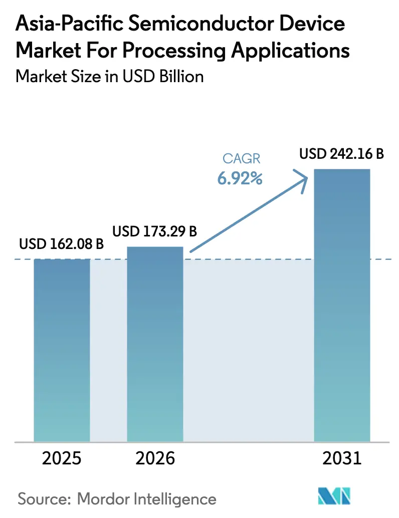
| Base Year Market Size (2025) | USD 162.08 Billion |
| Market Size (2026) | USD 173.29 Billion |
| Market Size (2031) | USD 242.16 Billion |
| Growth Rate (2026 - 2031) | 6.92% CAGR |
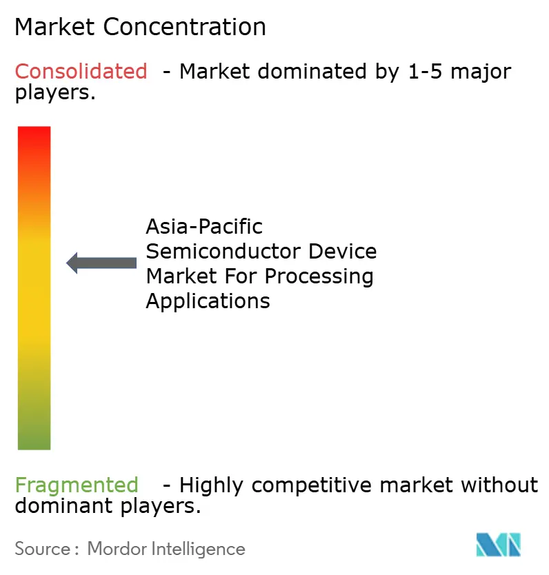
| Market Concentration | Medium |
Major Players *Disclaimer: Major Players sorted in no particular order Image © Mordor Intelligence. Reuse requires attribution under CC BY 4.0. | |
Analysis of Asia-Pacific Semiconductor Device Market For Processing Applications by Mordor Intelligence
The Asia-Pacific semiconductor device market size for processing applications was valued at USD 162.08 billion in 2025 and estimated to grow from USD 173.29 billion in 2026 to reach USD 242.16 billion by 2031, at a CAGR of 6.92% during the forecast period (2026-2031). Sovereign data-center buildouts, electric-vehicle mandates, and a healthy memory-cycle rebound underpin this growth, while export-control geopolitics and water scarcity shape investment decisions. Cloud providers are consolidating AI workloads onto denser accelerators, raising content per server and deepening reliance on advanced packaging. Automotive electrification is shifting silicon demand toward battery-management ICs and ADAS compute, tripling chip counts per vehicle compared with internal-combustion models. China remains the consumption anchor, yet India’s incentive-backed manufacturing push is lowering fab breakeven thresholds and diversifying regional capacity. At the same time, RISC-V cores are gaining momentum as buyers in China and India seek instruction-set sovereignty and lower licensing fees.
Key Report Takeaways
- By device type, integrated circuits led with a 45.12% of the Asia-Pacific semiconductor device market share in 2025, and they are on track for an 7.85% CAGR through 2031.
- By processing architecture, ARM-based designs held 72.45% of the Asia-Pacific semiconductor device market share in 2025, whereas RISC-V system-on-chips are poised for the fastest 8.48% CAGR to 2031.
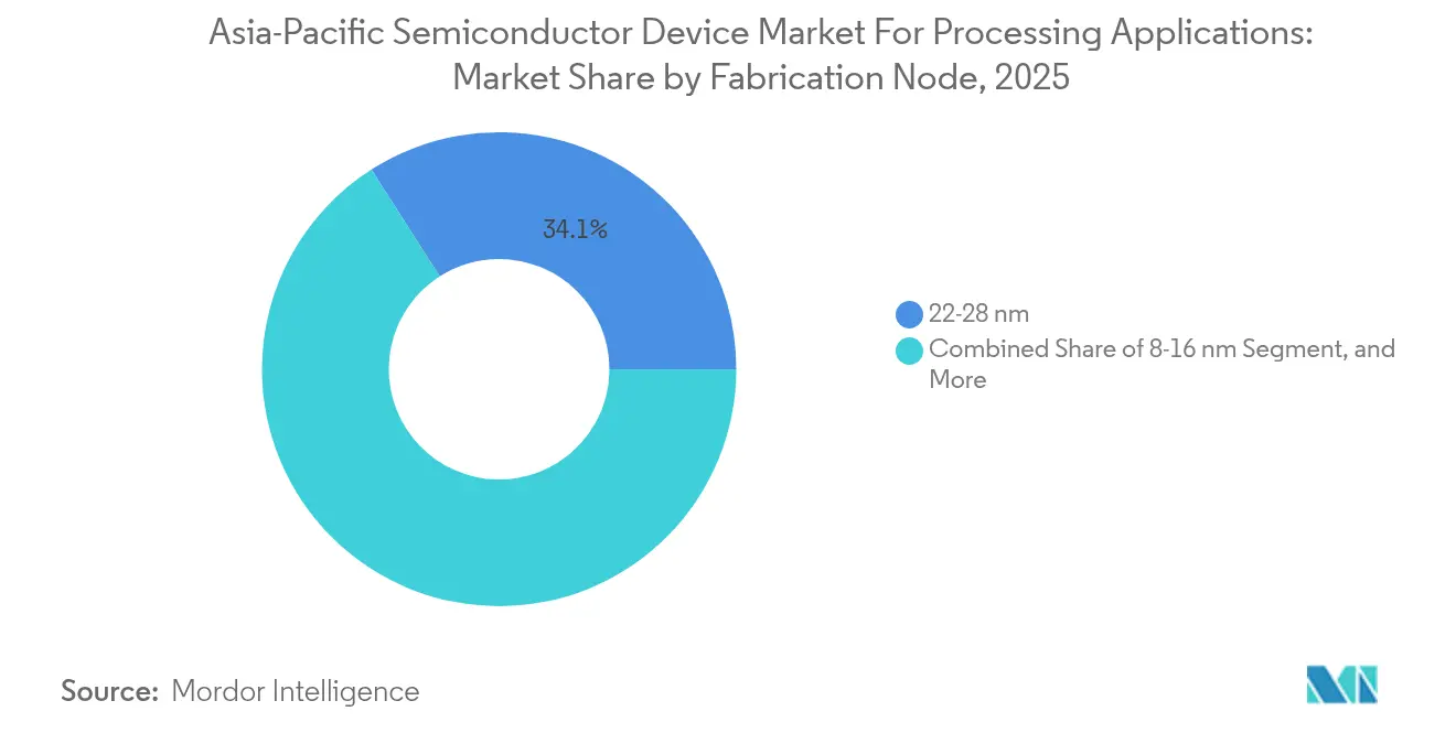
- By fabrication node, the 22 – 28 nanometer range controlled 34.05% of the Asia-Pacific semiconductor device market share in 2025, sub-3-nanometer processes will expand at a 7.55% CAGR as gate-all-around production ramps.
- By end-user industry, consumer electronics accounted for 37.15% of the Asia-Pacific semiconductor device market share in 2025, while automotive applications represent the quickest 7.78% CAGR through 2031.
- By geography, China commanded 51.35% share in 2025; India is forecast for the fastest 8.12% CAGR on the back of Production Linked Incentive disbursements.
Note: Market size and forecast figures in this report are generated using Mordor Intelligence’s proprietary estimation framework, updated with the latest available data and insights as of 2026.
Worldwide, activity is shaped by contributions from multiple regions, with Asia pacific representing one of the more structurally developed among them. The global report on semiconductor device for processing applications market by Mordor Intelligence reflects how these regional layers combine into a single system.
Insights and Trends of Asia-Pacific Semiconductor Device Market For Processing Applications
Drivers Impact Analysis*
| Driver | (~) % Impact on CAGR Forecast | Geographic Relevance | Impact Timeline |
|---|---|---|---|
| AI/ML and Data-centre Demand Surge | +1.8% | China, South Korea, Taiwan, Singapore | Medium term (2-4 years) |
| 5G-enabled IoT Device Proliferation | +1.2% | China, India, South Korea, Southeast Asia | Short term (≤ 2 years) |
| Government Fab Incentives Across Asia-Pacific | +1.5% | India, Japan, South Korea, Malaysia, Vietnam | Long term (≥ 4 years) |
| Memory-cycle Rebound and HBM Adoption | +1.3% | South Korea, Taiwan, Japan | Medium term (2-4 years) |
| RISC-V Localisation Push in China and India | +0.9% | China, India | Long term (≥ 4 years) |
| Edge-AI Modules for Smart Factories in SEA | +0.6% | Southeast Asia (Thailand, Vietnam, Indonesia) | Medium term (2-4 years) |
| Source: Mordor Intelligence | |||
AI/ML and Data-center Demand Surge
Generative-AI clusters deploy domain-specific accelerators that pair every GPU with eight HBM3 stacks, boosting memory ASPs and stressing advanced packaging capacity.[1]“HBM3E Mass Production Begins,” SK hynix Newsroom, skhynix.comTSMC increased CoWoS lines by 50% in 2024 and committed USD 11 billion for an additional site in Kumamoto to support 2.5D and 3D integration. Cloud operators are rolling out ARM-based Graviton and Ampere CPUs, which captured 28% of Asia-Pacific instance launches in 2024, underscoring the shift away from x86.[2]: “Graviton4 Instance Launch,” Amazon Web Services Blog, amazon.com China’s sovereign-AI mandate obliges local clouds to adopt domestically fabricated inference chips even at 14-nanometer nodes, redirecting demand toward SMIC and Huawei HiSilicon. Meanwhile, rack-power densities approaching 100 kW favor Singapore and Malaysia, where liquid-cooling infrastructure is colocated with chip-assembly operations.
5G-enabled IoT Device Proliferation
Asia-Pacific surpassed 2.1 billion cellular-IoT connections in 2024 as utilities deployed NB-IoT smart meters and logistics firms embedded Cat-M modules in cold-chain containers.[3]“NB-IoT Connections Forecast,” GSMA Intelligence, gsma.com Each endpoint carries three to five semiconductors, yet sub-USD 2 ASPs compress margins, pushing high-volume work to foundries running mature 28- and 40-nanometer lines. India’s 5G rollout covers 400 cities, driving demand for sub-6 GHz RF filters sourced from Taiwanese and Japanese specialists. Automotive telematics modules are migrating to 5G RedCap, a shift that benefits Renesas and NXP owing to functional-safety credentials.
Government Fab Incentives Across Asia-Pacific
India’s Semicon India program reimbursed 50% of capital expenditure in 2024, shrinking Micron’s Gujarat ATMP payback period from nine to just over five years. South Korea extended semiconductor-equipment tax credits to 25% and waived corporate income tax on greenfield fabs for a decade, supporting SK hynix’s KRW 120 trillion multi-cluster investment. Japan offered JPY 920 billion in grants for TSMC’s Kumamoto fabs, halving component lead times for local automotive clients. Malaysia and Vietnam provide 10-year corporate tax holidays on OSAT projects exceeding USD 500 million, drawing ASE and Amkor into advanced packaging.
Memory-cycle Rebound and HBM Adoption
DRAM ASPs surged 22% year-over-year in Q3 2024 as hyperscalers pre-ordered HBM3E stacks for 2025 AI servers. SK hynix now holds 53% of the HBM segment and has moved 28% of DRAM wafers to high-bandwidth products, while Samsung qualified 12-layer HBM3E for the NVIDIA B100 GPU after solving thermal-cycling issues. Micron began mass output of HBM3E in Q4 2024 and forecasts more than USD 8 billion in HBM revenue for fiscal 2025. NAND bit shipments increased 14% quarter-over-quarter as smartphones adopted 1-terabyte UFS 4.0 storage and enterprise SSDs transitioned to 232-layer designs, which lower the cost per bit by 18% compared to 176-layer nodes.
Restraints Impact Analysis*
| Restraint | (~) % Impact on CAGR Forecast | Geographic Relevance | Impact Timeline |
|---|---|---|---|
| Supply-chain Fragility and Material Shortages | -0.7% | Global, acute in Taiwan and South Korea | Short term (≤ 2 years) |
| Export-control Geopolitics on Advanced Tools | -1.1% | China, spillover to Southeast Asia | Medium term (2-4 years) |
| EUV-talent Bottleneck in Asia-Pacific Fabs | -0.5% | Taiwan, South Korea, Japan | Medium term (2-4 years) |
| Water-scarcity Risk at Leading Foundries | -0.4% | Taiwan, localized in Hsinchu and Tainan | Long term (≥ 4 years) |
| Source: Mordor Intelligence | |||
Export-control Geopolitics on Advanced Tools
The United States barred servicing of DUV immersion scanners at Chinese fabs in October 2024 and Japan restricted 23 classes of chip-equipment exports, forcing Chinese foundries to rely on multi-patterning at 14 nanometer nodes, lengthening wafer cycles and inflating cost-per-transistor by one-third. With TSMC and Samsung pre-ordering 62 High-NA EUV systems, ASML’s backlog stretches 18 months, leaving no near-term capacity for new entrants even if licenses loosen.
EUV-talent Bottleneck in Asia-Pacific Fabs
TSMC filled only 58% of its 1,450 EUV-engineering vacancies in 2024 as local universities graduate fewer than 800 semiconductor majors annually. Samsung offered 30% salary premiums to lure lithography engineers, driving a regional wage spiral that lifted fab operating costs 9% year-over-year. Japan’s Rapidus will rely on expatriates until domestic universities deliver a first cohort of 120 specialists in 2027.
*Our forecasts treat driver/restraint impacts as directional, not additive. The impact forecasts reflect baseline growth, mix effects, and variable interactions.
Segment Analysis
By Device Type: Integrated Circuits Dominate Value and Growth
Integrated circuits accounted for 45.12% of 2025 revenue within the Asia-Pacific semiconductor device market and will advance at an 7.85% CAGR through 2031, outpacing discretes as hyperscalers migrate from board-level to monolithic AI accelerators. Logic products lead the surge, with NVIDIA’s H200 on TSMC’s N3E node delivering 40% more TOPS-per-watt than its predecessor, pushing average wafer values higher.
Discrete semiconductors, optoelectronics, and sensors collectively held a 54.88% share; however, growth trails ICs at a 6.35% CAGR, as price competition dilutes ASP gains. Silicon-carbide device revenue is constrained by 150 mm wafer shortages, which stretch lead times to 52 weeks, while co-packaged optics trim the module bill of materials by 22%, compressing photonics margins.


By Processing Architecture: ARM Leads, RISC-V Disrupts
ARM designs commanded 72.45% share in 2025, powering smartphones, cloud servers and automotive compute, whereas RISC-V cores will expand at 8.48% CAGR as governments prioritize instruction-set autonomy.
The Asia-Pacific semiconductor device market size for RISC-V solutions is growing from a small base, benefiting from royalty-free licensing and rapidly maturing toolchains. Alibaba’s Xuantie C920 matched ARM Cortex-A76 integer performance at lower recurring fees, while India’s Shakti core delivers secure variants for defense avionics. In contrast, x86 clings to an 17.85% share confined to high-performance servers, posting the slowest 4.62% CAGR.
By Fabrication Node: Legacy Nodes Persist, Sub-3 nm Races Ahead
The 22 – 28 nanometer bracket retained 34.05% share in 2025, bolstered by power-management ICs and RF transceivers where leakage specs trump density. The Asia-Pacific semiconductor device market share for these legacy nodes remains sticky because automotive and industrial buyers value proven yields and AEC-Q100 grades.
Sub-3-nanometer capacity, however, shows a 7.55% CAGR as TSMC’s N2 and Samsung’s 2 nm gate-all-around deliver 15% speed gains and 25% power cuts versus N3E. Apple’s A19 and M5 chips will be first off TSMC’s N2 line in late 2025, while Samsung’s win of Qualcomm’s Snapdragon 8 Gen 4 restores credibility to its foundry roadmap.
By End-User Industry: Automotive Overtakes Consumer Electronics Growth
In 2025, consumer electronics dominated with a 37.15% share, while automotive applications are set to grow at the fastest pace, boasting an 7.78% CAGR through 2031. The Asia-Pacific semiconductor device market size for automotive applications is accelerating at an 7.78% CAGR as EV production in China hit 9.5 million units, and each vehicle now integrates up to 3,000 chips.
Battery-management ICs and ADAS compute drive the surge: a single electric vehicle embeds 12–18 power-management ICs and SoCs delivering 200–500 TOPS for sensor fusion. Data-center infrastructure holds an 17.85% share and grows at a 7.42% CAGR as AI clusters consume 35,000 GPUs per site, each paired with eight HBM stacks.
Geography Analysis
China captured 51.35% of 2025 revenue on the strength of 3.2 million 300 mm-equivalent wafer starts per month. SMIC added 120,000 14 nm FinFET starts, enabling Huawei to ship 60 million Kirin-based phones despite tool embargoes. The National Integrated Circuit Fund’s RMB 344 billion Phase III capital focuses on memory, compound semiconductors and EDA, accelerating domestic supply-chain depth. Design activity is concentrated in Shenzhen and Shanghai, which together hosted 1,890 fabless firms after venture capital invested USD 6.2 billion in AI-chip startups.
India is the fastest-growing geography at an 8.12% CAGR. Micron broke ground on a USD 2.75 billion Gujarat ATMP plant, while Tata Electronics integrated Wistron’s iPhone assets to add local packaging for Apple’s processors, trimming logistics lead times from three weeks to one. National OSAT capacity is forecast to reach 450,000 wafer equivalents per month by 2028, up from 80,000 in 2024, reflecting the commitment of lines from CG Power and Kaynes Technology.
South Korea held 20.55% share backed by Samsung and SK hynix, which delivered 68% of global DRAM in 2024. SK hynix invested KRW 18.6 trillion to scale HBM3E at its M16 fab, targeting 60% HBM share by 2026. Taiwan retained 16.95% share, anchored by TSMC’s 14 fabs that output 3.1 million 300 mm wafers monthly. Japan controlled 5.05% led by Renesas and Rohm, while Rapidus advances its 2 nm program. Singapore, Malaysia, Vietnam and Thailand collectively held 6.10%, specializing in OSAT and discrete power devices.
Competitive Landscape
The top five suppliers, TSMC, Samsung, SK hynix, Intel, and Micron, claimed most of the regional sales in 2024, evidencing a concentrated yet vigorously contested arena. TSMC sustained a 54% foundry share thanks to N3E yield leadership and CoWoS packaging that lowers inter-chip latency by 60% for customers such as NVIDIA and AMD. Samsung is investing USD 230 billion through 2042 to chase a 20% foundry share, but it must resolve gate-all-around yields that lag TSMC by 18 months. SK hynix has repurposed Intel’s former NAND fabs for HBM, while Micron is diversifying assembly to India and Malaysia to hedge geopolitical risk.
Chinese challengers escalate pressure: SMIC has produced the first-generation 7nm logic via multipatterning and domestic tools; its 120,000 wafers-per-month run rate signals that tool controls cannot fully arrest technology migration. Tata Electronics is building a vertically integrated chain from fabless design to OSAT, targeting 15% of India’s chip demand by 2028. Patent activity underscores the pivot toward chiplet architectures, the UCIe consortium logged 342 filings in 2024, foreshadowing the development of modular SoCs that can be tiled across different process nodes.
White-space opportunities emerge in edge-AI inference accelerators for smart-factory and automotive deployments requiring 2–8 W envelopes that big GPUs cannot reach. Start-ups such as Hailo and Kneron deliver 2–8 TOPS-per-watt devices priced under USD 10, riveting OEM interest.
Leaders of Asia-Pacific Semiconductor Device Market For Processing Applications
Intel Corporation
Nvidia Corporation
Kyocera Corporation
Qualcomm Incorporated
STMicroelectronics NV
- *Disclaimer: Major Players sorted in no particular order

Recent Industry Developments
- September 2025: Rapidus finished clean-room construction at its Chitose 2 nm logic fab and installed Japan’s first ASML High-NA EUV scanner, keeping the pilot-production target of late 2027 on schedule
- June 2025: Micron Technology opened its USD 1.6 billion DRAM assembly and test plant in Penang, Malaysia, bringing initial capacity of 120 million units per quarter and reducing regional back-end cycle time by 18%
- April 2025: Samsung Electronics completed risk production of its 2 nm gate-all-around node at the expanded Pyeongtaek Line 3, validating yields above 60% for Qualcomm’s Snapdragon 8 Gen 5 reference wafers
- January 2025: TSMC initiated high-volume production of its 2 nm N2 gate-all-around process at the new Fab 20 in Hsinchu, with the first Apple A19 application processors already shipped to assembly partners


Scope of Report on Asia-Pacific Semiconductor Device Market For Processing Applications
The Asia-Pacific semiconductor device market for processing applications report is Segmented by Device Type (Discrete Semiconductors, Optoelectronics, Sensors, Integrated Circuits), Processing Architecture (x86, ARM, RISC-V, MIPS and Other Other Processing Architectures), Fabrication Node (Below 7 nm, 8–16 nm, 22–28 nm, Above 32 nm), End-User Industry (Consumer Electronics, Automotive, Industrial and Manufacturing, Data Centre and Cloud, Telecommunications, Healthcare Devices, Aerospace and Defence, Other End-User Industries), and Geography (China, India, Japan, South Korea, Taiwan, Singapore, Rest of Asia-Pacific). The Market Forecasts are Provided in Terms of Value (USD).
| Discrete Semiconductors | |
| Optoelectronics | |
| Sensors | |
| Integrated Circuits | Analog |
| Logic | |
| Memory | |
| Micro |
| x86 |
| ARM |
| RISC-V |
| MIPS and Other Processing Architectures |
| Below 7 nm (N7, N5, N3 and below) |
| 8–16 nm |
| 22–28 nm |
| Above 32 nm (Legacy and Specialty) |
| Consumer Electronics |
| Automotive |
| Industrial and Manufacturing |
| Data Centre and Cloud |
| Telecommunications |
| Healthcare Devices |
| Aerospace and Defence |
| Other End-User Industries |
| China |
| India |
| Japan |
| South Korea |
| Taiwan |
| Singapore |
| Rest of Asia-Pacific |
| By Device Type | Discrete Semiconductors | |
| Optoelectronics | ||
| Sensors | ||
| Integrated Circuits | Analog | |
| Logic | ||
| Memory | ||
| Micro | ||
| By Processing Architecture | x86 | |
| ARM | ||
| RISC-V | ||
| MIPS and Other Processing Architectures | ||
| By Fabrication Node | Below 7 nm (N7, N5, N3 and below) | |
| 8–16 nm | ||
| 22–28 nm | ||
| Above 32 nm (Legacy and Specialty) | ||
| By End-User Industry | Consumer Electronics | |
| Automotive | ||
| Industrial and Manufacturing | ||
| Data Centre and Cloud | ||
| Telecommunications | ||
| Healthcare Devices | ||
| Aerospace and Defence | ||
| Other End-User Industries | ||
| By Country | China | |
| India | ||
| Japan | ||
| South Korea | ||
| Taiwan | ||
| Singapore | ||
| Rest of Asia-Pacific | ||


Key Questions Answered in the Report
What is the 2026 value of the Asia Pacific semiconductor device market?
The market is estimated at USD 173.29 billion in 2026.
How fast will automotive demand grow?
Automotive semiconductor revenue in the region is forecast to rise at an 7.78% CAGR through 2031.
Which node currently leads in wafer output?
The 22 – 28 nanometer range holds the largest 34.05% fabrication share.
Who dominates advanced packaging?
TSMC commands the lead after boosting CoWoS capacity 50% and adding a new plant in Japan.
Why is RISC-V gaining traction in Asia Pacific?
Governments in China and India favor RISC-V to avoid ARM royalties and achieve instruction-set autonomy, supporting an 8.48% CAGR.
Page last updated on:


