Additive Manufacturing In Semiconductor Market Size and Share
Market Overview
| Study Period | 2020 - 2031 |
|---|---|
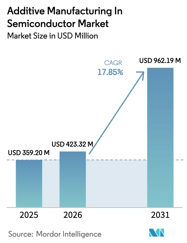
| Market Size (2026) | USD 423.32 Million |
| Market Size (2031) | USD 962.19 Million |
| Growth Rate (2026 - 2031) | 17.85% CAGR |
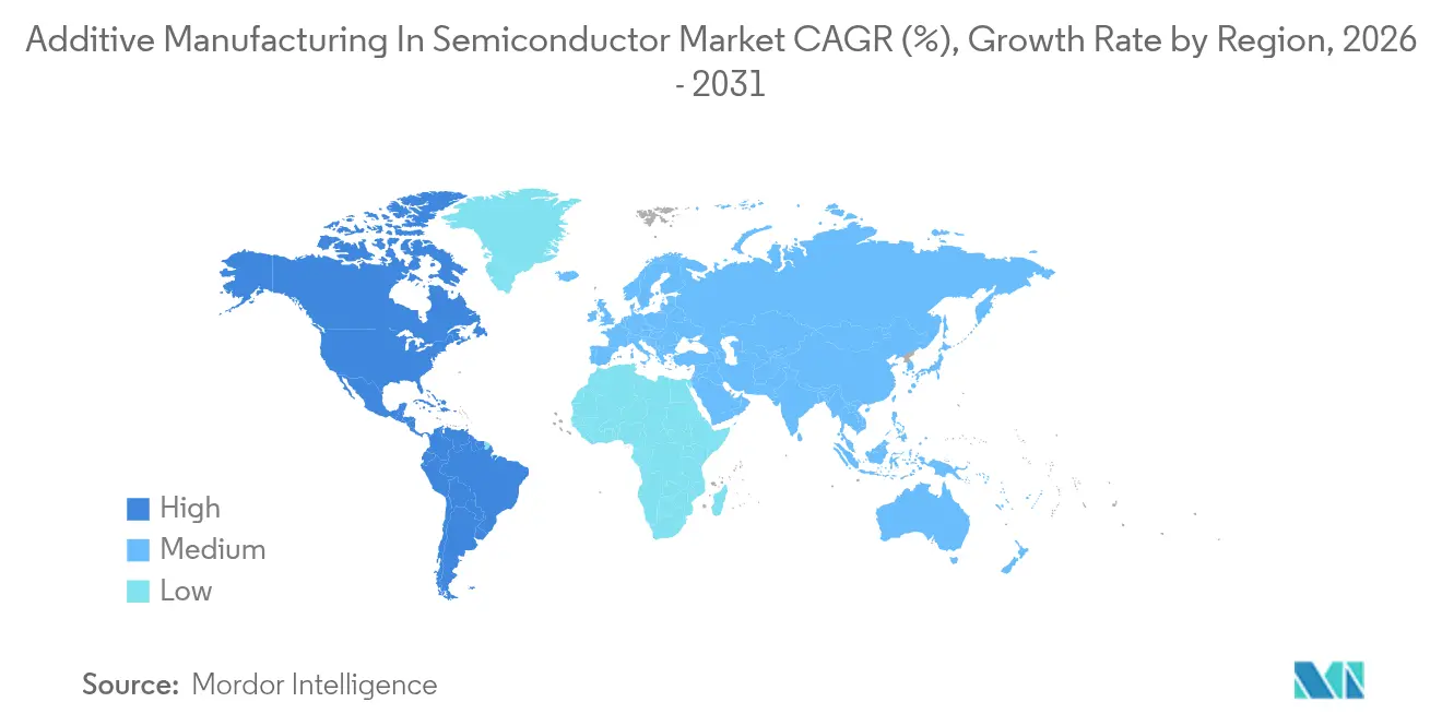
| Fastest Growing Market | North America |
| Largest Market | Asia Pacific |
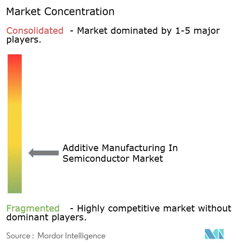
| Market Concentration | Low |
Major Players *Disclaimer: Major Players sorted in no particular order Image © Mordor Intelligence. Reuse requires attribution under CC BY 4.0. | |
Additive Manufacturing In Semiconductor Market Analysis by Mordor Intelligence
The additive manufacturing in semiconductor market size was valued at USD 359.2 million in 2025 and estimated to grow from USD 423.32 million in 2026 to reach USD 962.19 million by 2031, at a CAGR of 17.85% during the forecast period (2026-2031). Vendors are pivoting toward precision three-dimensional printing to insulate supply chains, shorten design cycles, and support the demanding geometries of next-generation lithography, deposition, and advanced packaging tools. Adoption accelerates where conventional subtractive methods stall especially in high-vacuum wafer-fab environments that require intricate cooling channels, low-contamination materials, and fast design iteration. Capital equipment makers now treat additive processes as native production tools rather than experimental pilots, integrating them directly into lithography optic modules, gas manifolds, and wafer-handling robotics. Metals still dominate build volumes, yet technical ceramics, ultra-pure nickel alloys, and specialty photopolymers are expanding the reachable application set. Regional momentum is strongest in Asia–Pacific, where Taiwan and Japan pair deep fabrication know-how with government incentives, while North American and European reshoring programs stimulate on-shore capacity and South America positions itself as a future low-cost equipment hub.
Key Report Takeaways
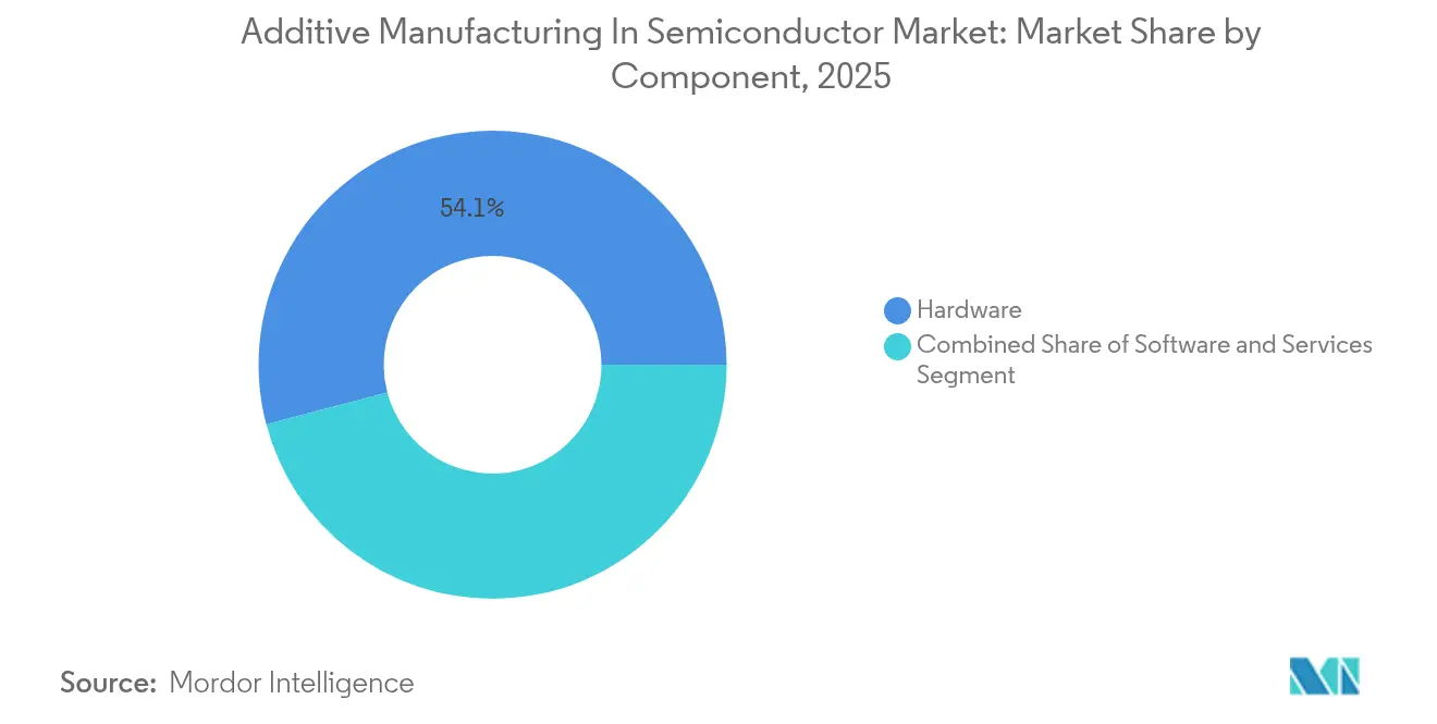
- By component, hardware captured 54.10% revenue share in 2025; software is forecast to grow at an 18.34% CAGR to 2031.
- By material, metals and alloys held 46.20% of the additive manufacturing in semiconductor market share in 2025, while technical ceramics are set to expand at 21.95% CAGR through 2031.
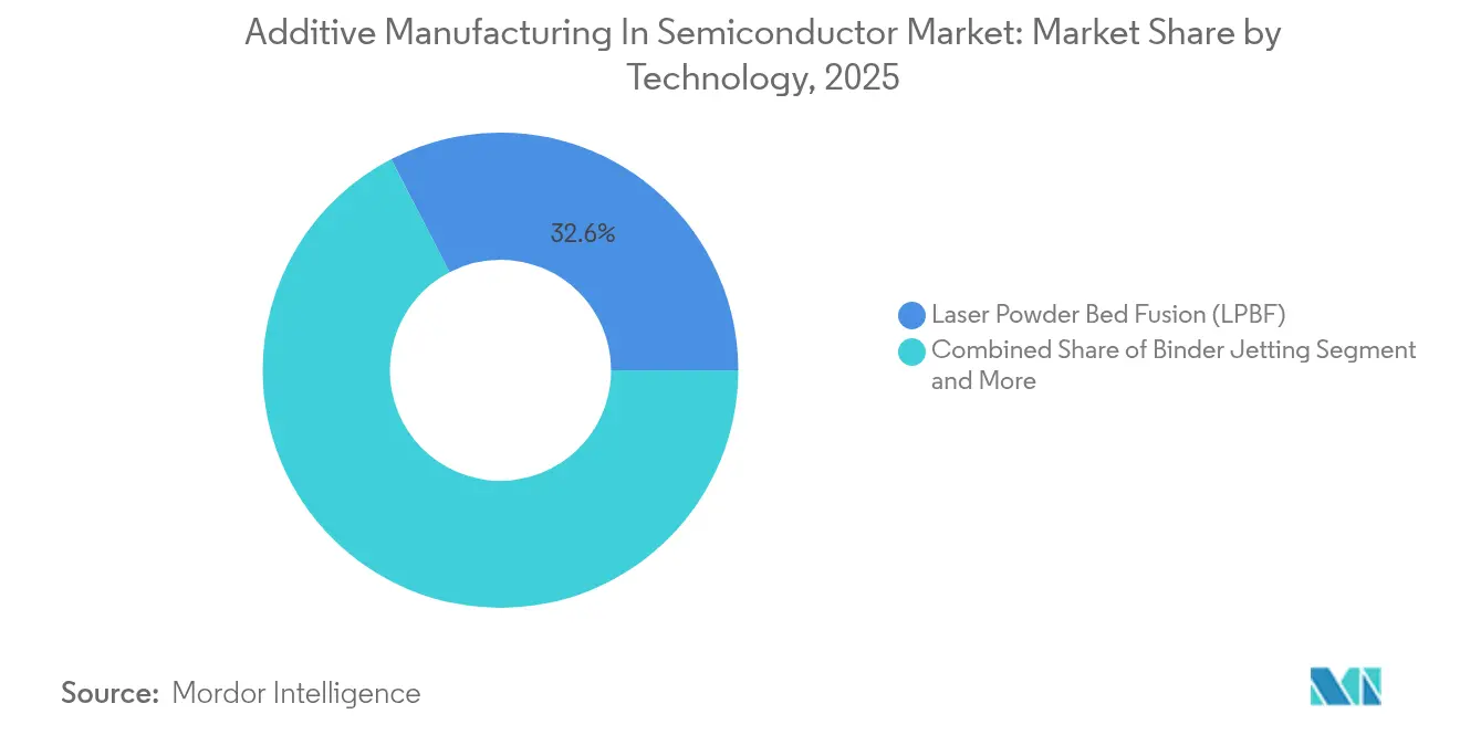
- By technology, LPBF led with 32.60% share in 2025; PµSL is projected to rise at a 24.12% CAGR to 2031.
- By process stage, wafer-fabrication components accounted for 41.00% share of the additive manufacturing in semiconductor market size in 2025, whereas packaging and assembly parts advance at a 20.25% CAGR.
- By end-use equipment, lithography systems commanded 28.70% share in 2025; wafer-handling and robotics equipment grows fastest at 19.55% CAGR.
- By region, APAC maintained 43.20% share in 2025; South America records the highest 19.20% CAGR to 2031.
Note: Market size and forecast figures in this report are generated using Mordor Intelligence’s proprietary estimation framework, updated with the latest available data and insights as of 2026.
Global Additive Manufacturing In Semiconductor Market Trends and Insights
Drivers Impact Analysis*
| Driver | (~) % Impact on CAGR Forecast | Geographic Relevance | Impact Timeline |
|---|---|---|---|
| Rapid prototyping demand in semiconductor capital equipment | +4.2% | Global with APAC and North America focus | Short term (≤ 2 years) |
| Miniaturization and complex-geometry requirements | +3.8% | Taiwan, Korea, United States fabs | Medium term (2-4 years) |
| Supply-chain resiliency amid chip shortages | +3.1% | North America and Europe priorities | Medium term (2-4 years) |
| High-performance metal and ceramic breakthroughs | +2.9% | Global R&D hubs | Long term (≥ 4 years) |
| AM-enabled heterogeneous integration and packaging | +2.4% | APAC-centric, expanding to North America | Medium term (2-4 years) |
| Government reshoring incentives for on-shore AM fabs | +1.8% | United States, European Union, Japan | Long term (≥ 4 years) |
| Source: Mordor Intelligence | |||
Rapid prototyping demand in semiconductor capital equipment
Equipment suppliers are under pressure to slash tool development cycles from 18-24 months to 6-12 months. ASMPT’s deployment of the FUNMAT PRO 310 NEO cut prototype lead time and cost by over 50%, letting engineers iterate on tooling, fixtures, and end-use metal parts within weeks. That advantage is vital for EUV lithography modules where cooling channels are too convoluted for milling.[2]ZEISS SMT, “EUV Lithography and Technology,” zeiss.com Demonstrations at SEMICON Japan 2024 showed Toray Industries producing stainless manifolds for plasma reactors in days, validating additive’s time-to-market edge.
Miniaturization & complex-geometry requirements
Gate-all-around transistors, 3D NAND structures, and chiplet-based packages force equipment to support sub-micron alignment and exotic fluid routing. Applied Materials notes hundreds of etch–deposit cycles per wafer; these demand injector arrays and shielding components with internal lattices that conventional machining cannot form. Projection Micro-Stereolithography achieves 0.6 µm resolution, fabricating test sockets and MEMS fixtures that integrate directly into advanced metrology stages. Such capability is central to ultra-high-vacuum wafer-handling robots.
Supply-chain resiliency amid chip shortages
The pandemic-era chip crunch exposed vulnerabilities in single-source component supply. Equipment builders now deploy dispersed additive nodes to localize production and reduce logistics risk. Hittech Bihca’s switch to rapid plasma deposition for carrier trays delivered near-net geometries while trimming 90% material waste, a template for distributed manufacturing. United States CHIPS incentives and European subsidy packages accelerate domestic AM cell installations, reinforcing this driver.
High-performance metal & ceramic material breakthroughs
Laser-sintered hafnium carbide, demonstrated by North Carolina State University, cuts production time from hours to minutes while boosting yield to 50%, opening paths for plasma-facing parts in etchers that run above 3,500 °C. EOS’s NiCP alloy eliminates secondary nickel plating on gas injectors and extends tool uptime. These material gains expand additive’s viable part list.
Restraints Impact Analysis*
| Restraint | (~) % Impact on CAGR Forecast | Geographic Relevance | Impact Timeline |
|---|---|---|---|
| High upfront cost of industrial metal AM systems | -2.8% | Global, hardest on SMEs in emerging markets | Short term (≤ 2 years) |
| Lack of semiconductor-grade AM standards & QA protocols | -2.1% | Worldwide gap, acute in tightly regulated markets | Medium term (2-4 years) |
| Contamination risk inside ultra-clean wafer fabs | -1.7% | Global cleanrooms, critical in advanced-node fabs | Medium term (2-4 years) |
| Limited portfolio of ultra-pure, low-outgassing AM materials | -1.4% | Global, focused on high-purity applications | Long term (≥ 4 years) |
| Source: Mordor Intelligence | |||
High upfront cost of industrial metal AM systems
Production-class metal printers suited to semiconductor tolerances exceed USD 500,000 per unit, and often approach USD 2 million once post-processing, inert-gas infrastructure, and metrology are included. Nikon’s 2025 results underscore how smaller firms struggle to justify those assets outside aerospace or defense, prompting the OEM to concentrate on large-format LPBF where volumes warrant the expense. Service-based models such as Velo3D’s Rapid Production Solutions, which targets a 40% revenue share by 2026, show promise in reducing capital outlays.
Lack of semiconductor-grade AM standards & QA protocols
Cleanroom parts require strict outgassing, particle, and ionic contamination controls, yet industry-wide qualification frameworks for additive builds remain nascent. Studies confirm that 3D-printed polymers can match particle emission levels of conventional equivalents, but no formal schema ties material selection, build parameters, and inspection to International Technology Roadmap requirements. PFAS polymer restrictions further complicate certification, and although ALD coatings mitigate outgassing, documented acceptance tests are still pending. Until consensus standards emerge, OEMs must navigate bespoke validation, elongating adoption timetables.
*Our forecasts treat driver/restraint impacts as directional, not additive. The impact forecasts reflect baseline growth, mix effects, and variable interactions.
Segment Analysis
By Component: Hardware integration reshapes tool manufacturing
Hardware represented 54.10% of revenue in 2025, confirming that production-scale printers, powder-handling stations, and in-situ monitoring sensors remain the primary spending focus. Equipment OEMs integrate multi-laser LPBF cells directly onto factory floors to print wafer-stage brackets, thermal spreaders, and custom vacuum fittings, turning additive lines into just-in-time spare-part depots. Software contributes the sharpest growth at an 18.34% CAGR as build-parameter optimization, real-time defect detection, and generative design accelerate design-for-additive workflows. Services close capability gaps for fabs lacking in-house additive engineers, pairing material selection with contamination consulting.
The software wave reflects rising part complexity and stringent documentation. Build-prep suites now embed topology optimization that routes coolant through organic channels impossible via CNC. Process-control dashboards harness machine-learning to predict pore formation and adjust laser parameters on the fly, pushing yield upward. As these platforms mature, subscription-based licensing and cloud analysis diminish cost barriers, fueling deployment across mid-tier toolmakers and contributing to the additive manufacturing in semiconductor market expansion.


By Material: Ceramics outpace metal dominance
Metals and alloys delivered 46.20% of 2025 spend, rooted in stainless, Inconel, copper, and Ti-6Al-4V parts for high-vacuum environments. Ceramics posted the highest 21.95% CAGR, propelled by hafnium carbide divergence nozzles and 99.99% alumina shields used in aggressive plasma chambers. Polymers like PEEK and PEKK fulfill static jigs and ESD-safe tooling roles, while metal–polymer composites improve stiffness-to-weight for robot arms.
Technical ceramics’ rise draws on laser-assisted printing processes that sinter dense features without lengthy furnace cycles. The resulting ultra-pure surfaces meet ionic cleanliness targets, broadening use in component slots where metals risk contaminating wafers. Material innovators focus on powder purity and controlled grain structures, appealing to fabs that equate surface integrity with yield. Such progress underpins the additive manufacturing in semiconductor market size growth, particularly in critical process chambers.
By Technology: PµSL pushes sub-micron frontiers
LPBF retained 32.60% share in 2025 thanks to its ability to form fully dense nickel or copper at productivity levels suitable for serial builds. Projection Micro-Stereolithography’s 24.12% CAGR highlights the value of 0.6 µm resolution when crafting micro-grippers, MEMS test sockets, and fluidic manifolds. SLA and FDM provide fast polymer mock-ups, while binder jetting gains traction for large porous ceramic filters and direct energy deposition serves repair and gradient-material tasks.
PµSL adoption aligns with metrology’s miniaturization. Digital micromirror devices project patterns enabling thousands of features printed concurrently, which slashes cycle time for micro-nozzle arrays. Patent filings around far-field superlens optics hint at future 100 nm voxel sizes, foreshadowing deeper equipment integration. These technology shifts reinforce competitive differentiation within the additive manufacturing in semiconductor market.
By Semiconductor Process Stage: Advanced packaging surges
Wafer-fab components comprised 41.00% usage in 2025, but packaging and assembly elements show a 20.25% CAGR as chiplet integration drives exotic interconnects. Complex socket frames, thermal bridges, and interposer carriers rely on lattice infills for stiffness and reduced weight. Metrology and test fixtures benefit from captive-channel cooling, and cleanroom tools pivot to polymer prints that cut cost by 90-99% versus machined stainless.
The additive manufacturing in semiconductor market share tied to packaging climbs because 3D silicon stacking magnifies heat density. Printed metal cold plates with conformal vanes dissipate thermal loads without enlarging footprint. Government funding, such as NIST’s USD 1.55 billion for advanced packaging R&D, positions additive as a default route for prototype hardware and low-volume production.
By End-use Equipment Type: Robotics adoption accelerates
Lithography systems accounted for 28.70% of revenue in 2025, embedding additive parts within high-NA optic housings and temperature-controlled stages. Wafer-handling and robotics modules grow at 19.55% CAGR as 450 mm wafers and EUV throughput push automation. Deposition and etch tools print corrosion-resistant injectors, while inspection stations adopt lightweight carbon-fiber-reinforced brackets to dampen vibration.
Robotics growth stems from the drive for fully automated fab lines by 2028 under initiatives like Japan’s SATAS consortium. Additively manufactured arms integrate hollow structures for vacuum routing, trimming mass and improving cycle time. Such performance increments directly influence fab cost of ownership and bolster the additive manufacturing in semiconductor market size trajectory.
Geography Analysis
Asia–Pacific held 43.20% share in 2025, fueled by Taiwan’s USD 65 billion investment pipeline and Japan’s JPY 3.9 trillion subsidy package, which embed printers inside tool-vendor production cells. South Korea’s USD 38.9 billion memory expansion adds orders for high-precision printed jigs and vacuum manifolds. Supply ecosystems cluster around Hsinchu and Kumamoto, where proximity supports same-day part fabrication and design turnover, reinforcing regional leadership of additive manufacturing in the semiconductor market.
North America expands steadily under CHIPS funding and state-level incentives. Intel’s Ohio and Arizona fabs bring in dedicated LPBF bays for optics mounts, while contract manufacturers in Oregon print copper heat exchangers destined for EUV mirrors. The European Union emphasizes sovereignty, with Dresden’s upcoming plant integrating AM for cold-plate prototypes and with ASML’s Dutch facilities scaling ceramic printing for optic barrel liners. Together these moves lift the additive manufacturing in semiconductor market across both regions.
South America posts the fastest 19.20% CAGR through 2031. Brazil’s policy to localize semiconductor tooling incentivizes additive adoption because it circumvents tooling imports and accelerates skills transfer. Pilot programs pair state funding with joint ventures from Taiwanese suppliers, creating a pathway for on-shore equipment fabrication. Israel and the Gulf states develop niche AM capabilities for specialty metrology arms, although broader adoption awaits regulatory harmonization and cleanroom infrastructure.

Competitive Landscape
The market remains moderately fragmented, with top players controlling meaningful yet non-dominant shares. 3D Systems, EOS, and Stratasys leverage decades of process tuning to supply LPBF and SLA platforms certified for cleanroom deployment. Boston Micro Fabrication and Lithoz target sub-micron ceramic niches where feature accuracy trumps build volume. Hardware incumbents increasingly collaborate with semiconductor toolmakers: ASMPT’s tie-up with INTAMSYS embeds printer clusters next to pick-and-place lines, trimming lead times.
Equipment OEMs such as ASML, Applied Materials, and Lam Research internalize additive cell capacity, a strategic move to protect intellectual property and assure part availability. Patent filings from Relativity Space on adaptive control illustrate the race toward fully autonomous laser parameter tuning, a capability that may spill into semiconductor printer fleets. Velo3D’s service-centric model competes on reduced capital exposure and on the ability to replicate qualified prints across its foundry network, a compelling approach for fabs avoiding printer ownership.
Competitive advantage also arises from material science. EOS’s NiCP alloy removes electroless plating steps, affording process cleanliness certifications that rival metal parts cannot always meet. Start-ups advancing low-outgassing polymers, like Dynamism’s Tullomer, gain traction in ultra-high vacuum tooling. As players specialize, the additive manufacturing in semiconductor market favors suppliers who couple material, software, and contamination expertise into turnkey solutions.
Additive Manufacturing In Semiconductor Industry Leaders
3D Systems Corporation
EnvisionTEC GmbH
Materialise NV
Optomec Inc.
General Electric Company (GE Additive)
- *Disclaimer: Major Players sorted in no particular order

Recent Industry Developments
- May 2025: Tekna recorded a 73% rise in AM powder orders, hiring a CEO with 30-year semiconductor pedigree.
- May 2025: ACM Research secured the 3D InCites Technology Enablement Award for panel-level packaging tool innovations.
- March 2025: EOS introduced NiCP alloy targeting semiconductor gas injectors.
- November 2024: TSMC secured USD 6.6 billion in CHIPS funding for Arizona fabs, spurring localized additive procurement


Research Methodology Framework and Report Scope
Market Definitions and Key Coverage
Our study defines the additive manufacturing in semiconductor industry market as all revenue generated by purpose-built hardware, software, materials, and related services that 3-dimensionally print parts, tooling, or sub-assemblies subsequently installed in wafer-fabrication, packaging, or test equipment.
Scope exclusion: Low-cost desktop printers and generic printed-electronics bureaus that never integrate with semiconductor capital equipment are excluded.
Segmentation Overview
- By Component
- Hardware
- Desktop 3D Printers
- Industrial 3D Printers
- Software
- Design Software
- Inspection and QA Software
- Printer Control Software
- Scanning/Reverse-Engineering Software
- Services
- Design and Prototyping Services
- Maintenance, Training and Consulting
- Hardware
- By Material
- Polymers
- Metals and Alloys
- Technical Ceramics
- Composites and Nanomaterial-Enhanced Resins
- By Technology
- Stereolithography (SLA)
- Fused Deposition Modeling (FDM)
- Laser Powder Bed Fusion (LPBF)
- Binder Jetting
- Direct Energy Deposition (DED)
- Projection Micro-Stereolithography and Other Emerging
- By Semiconductor Process Stage
- Wafer-fabrication Equipment Components
- Packaging and Assembly Components
- Test and Metrology Fixtures
- Clean-room Tooling and Jigs
- By End-use Equipment Type
- Lithography Systems
- Deposition and Etch Tools
- Wafer Handling and Robotics
- Thermal Processing Equipment
- Inspection and Metrology Tools
- By Geography
- North America
- United States
- Canada
- Mexico
- Europe
- United Kingdom
- Germany
- France
- Italy
- Rest of Europe
- Asia-Pacific
- China
- Japan
- India
- South Korea
- Rest of Asia
- Middle East
- Israel
- Saudi Arabia
- United Arab Emirates
- Turkey
- Rest of Middle East
- Africa
- South Africa
- Egypt
- Rest of Africa
- South America
- Brazil
- Argentina
- Rest of South America
- North America
Detailed Research Methodology and Data Validation
Primary Research
Mordor analysts interviewed equipment engineers in Taiwan, European alloy suppliers, and North American contract manufacturers, then surveyed clean-room AM machine vendors. These discussions clarified throughput targets, yield thresholds, and realistic penetration timelines, letting us refine secondary inputs and adjust price erosion curves.
Desk Research
We tapped public datasets from SEMI, UN Comtrade shipment codes for lithography tools, and Bureau of Industry & Security export filings to map global equipment flows. Company 10-Ks, earnings calls, and investor slides revealed average selling prices, while D&B Hoovers and Dow Jones Factiva furnished segment splits and currency-adjusted revenues. Peer-reviewed papers on laser powder bed fusion and projection micro-stereolithography, plus patent families accessed through Questel, highlighted emerging material mixes and feature size thresholds. The sources named are illustrative; numerous additional references underpinned data collection, validation, and clarification.
Market-Sizing & Forecasting
A top-down build anchored on annual wafer fab tool shipments, backend capital expenditure, and regional subsidy outlays was corroborated with selective bottom-up roll-ups of metal and ceramic powder demand. Key variables, EUV system backlogs, average layer counts per chiplet, AM hardware utilization rates, and semiconductor-grade ceramic powder ASPs, drive each yearly value. We applied multivariate regression with scenario analysis to project the market over the forecast period. Data gaps in supplier revenue were patched by triangulating interview ranges with regional proxy ratios.
Data Validation & Update Cycle
Outputs pass variance screens against historical series, anomaly flags, and a two-step analyst review. Reports refresh annually, with interim updates whenever subsidy shifts, material price shocks, or major capacity announcements materially alter the baseline.
Why Mordor's Additive Manufacturing In Semiconductor Baseline commands reliability
Published estimates often diverge because firms select different process stages, bundle printed electronics, or apply contrasting adoption curves.
Key gap drivers span scope breadth, conversion of powder tonnage to value, forecast cadence, and currency translation choices.
Benchmark comparison
| Market Size | Anonymized source | Primary gap driver |
|---|---|---|
| USD 359.2 million (2025) | Mordor Intelligence | - |
| USD 266.7 million (2025) | Regional Consultancy A | Omits packaging stage and ceramic inputs |
| USD 1.47 billion (2024) | Global Forecast Service B | Bundles printed electronics and polymers, includes internal R&D spend |
| USD 160 million (2024) | Trade Journal C | Covers early adopter fabs in two regions with a conservative penetration curve |
The comparison shows that by selecting a precise value chain scope, blending top down with bottom up checks, and maintaining an annual refresh, Mordor Intelligence delivers a balanced, transparent baseline that decision makers can confidently trace and replicate.


Key Questions Answered in the Report
What is the current value of the additive manufacturing in semiconductor market?
The market stands at USD 423.32 million in 2026 and is forecast to reach USD 962.19 million by 2031.
Which segment grows fastest within this market?
Software solutions register the highest 18.34% CAGR as fabs invest in design-optimization and in-situ quality control platforms.
Why are technical ceramics gaining popularity?
Ceramics like hafnium carbide and high-purity alumina withstand extreme plasma and temperature conditions that traditional metals cannot, leading to a 21.95% CAGR for this material category.
Which region leads market revenue?
Asia–Pacific holds 43.20% share owing to the concentrated semiconductor ecosystems in Taiwan, Japan, and South Korea.
How is additive manufacturing improving semiconductor supply-chain resilience?
By enabling localized, on-demand production of complex parts, additive manufacturing reduces reliance on single-source suppliers and mitigates logistics disruptions revealed during recent chip shortages.
What is the main barrier to wider adoption?
High capital costs for industrial metal printers—often exceeding USD 500,000—combined with the absence of standardized cleanroom qualification protocols slow uptake among smaller equipment makers.
Page last updated on:


