Wafer Prober Market Size and Share
Market Overview
| Study Period | 2020 - 2031 |
|---|---|
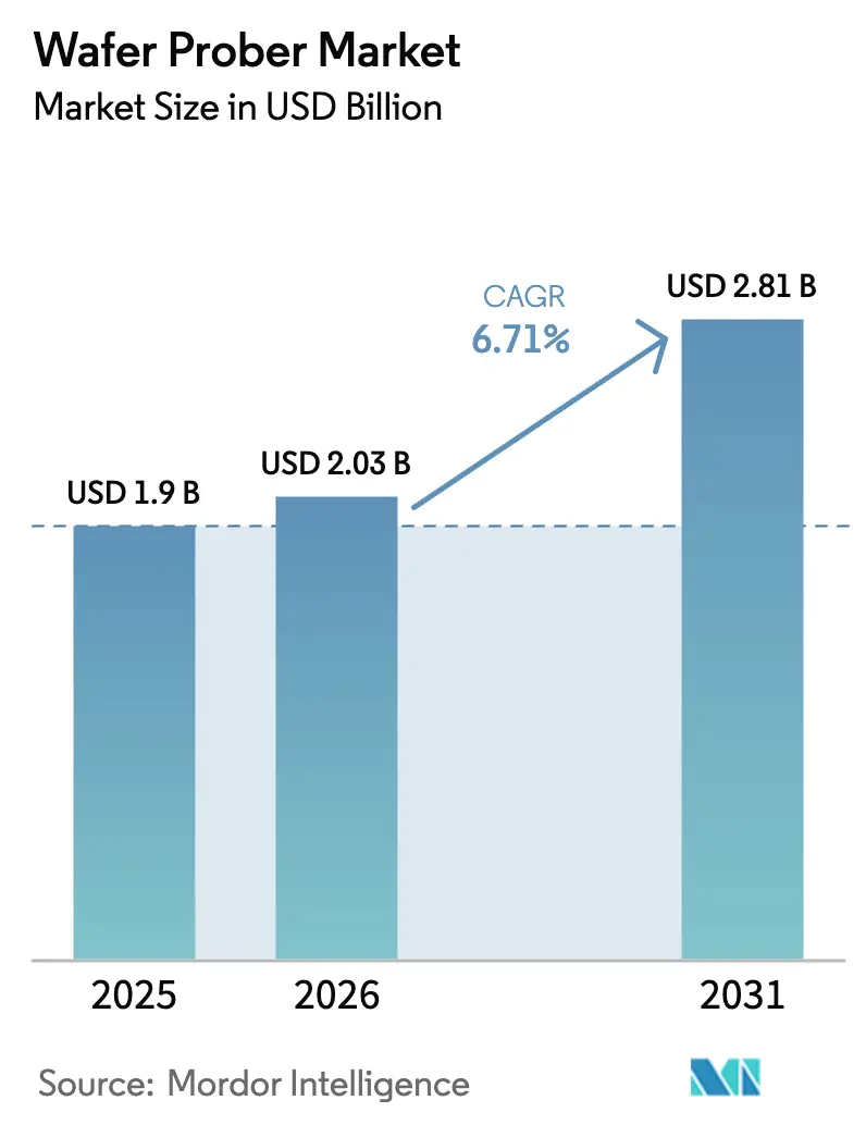
| Market Size (2026) | USD 2.03 Billion |
| Market Size (2031) | USD 2.81 Billion |
| Growth Rate (2026 - 2031) | 6.71% CAGR |
| Fastest Growing Market | Middle East and Africa |
| Largest Market | Asia Pacific |
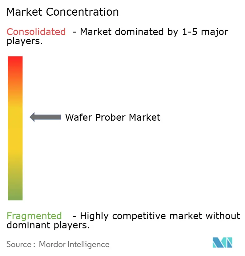
| Market Concentration | Medium |
Major Players *Disclaimer: Major Players sorted in no particular order Image © Mordor Intelligence. Reuse requires attribution under CC BY 4.0. | |
Wafer Prober Market Analysis by Mordor Intelligence
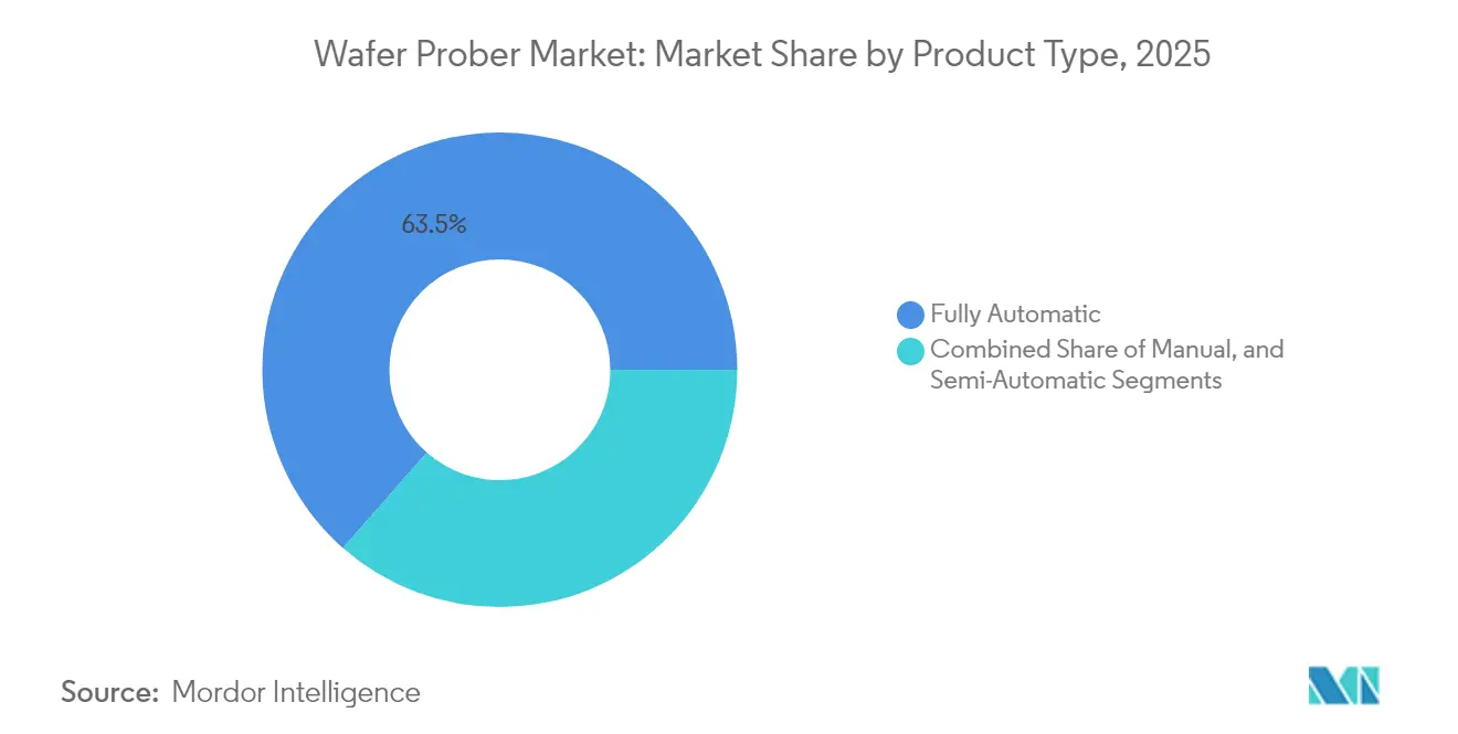
The wafer prober market size in 2026 is estimated at USD 2.03 billion, growing from 2025 value of USD 1.90 billion with 2031 projections showing USD 2.81 billion, growing at 6.71% CAGR over 2026-2031. This solid growth links directly to the semiconductor sector’s rising production capacity and the need to validate ever-smaller, higher-performance chips before packaging. High-volume adoption of advanced packaging, the surge in AI and 5G device output, and the transition to larger wafer formats each reinforce demand for next-generation wafer probers. Vendors are responding by embedding AI in fault detection, integrating predictive maintenance, and improving probe-card precision to keep throughput high and test costs low. The fully automatic segment leads with a 64.1% wafer prober market share in 2024, aided by factory-wide automation programs that target lights-out manufacturing. Contact-based probers still dominate day-to-day test floors, holding 87.2% share, yet non-contact RF solutions are scaling fast to support sub-THz devices.
Key Report Takeaways
- By product type, fully automatic probers held 63.52% wafer prober market share in 2025; semi-automatic systems are forecast to expand at a 9.03% CAGR through 2031.
- By technology, contact-based units retained 86.55% revenue share in 2025, while non-contact methods are projected to post a 13.56% CAGR to 2031.
- By application, wafer sort/CP accounted for 57.62% of the wafer prober market size in 2025; R&D/failure analysis is advancing at a 14.22% CAGR.
- By wafer size, the 200-300 mm bracket held 69.72% of the wafer prober market size in 2025, whereas >300 mm panels are forecast to climb at an 18.58% CAGR.
- By end-user, foundries commanded 45.98% share of the wafer prober market size in 2025; research and academia exhibit a 14.91% CAGR to 2031.
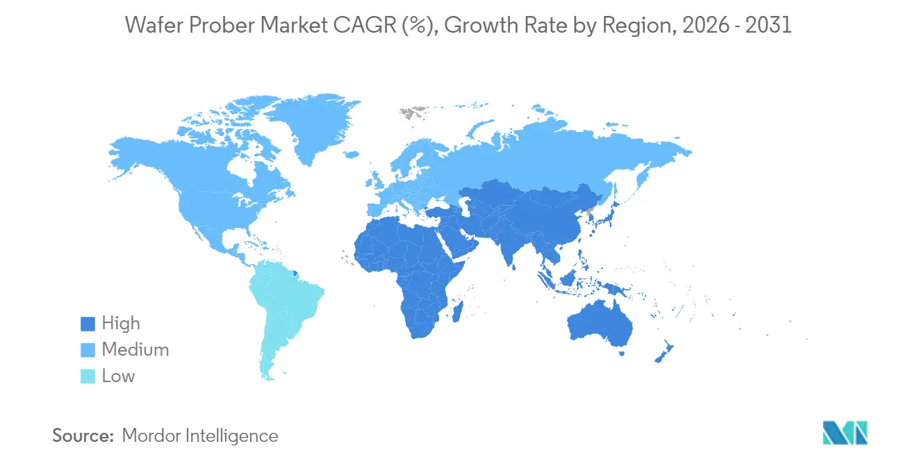
- By geography, Asia-Pacific led with 47.05% of the wafer prober market size in 2025; the Middle East is expanding at an 11.24% CAGR through 2031.
Note: Market size and forecast figures in this report are generated using Mordor Intelligence’s proprietary estimation framework, updated with the latest available data and insights as of 2026.
Global Wafer Prober Market Trends and Insights
Drivers Impact Analysis*
| Driver | (~) % Impact on CAGR Forecast | Geographic Relevance | Impact Timeline |
|---|---|---|---|
| 3-D IC and advanced packaging boom | +2.1% | Global, concentrated in Asia-Pacific | Medium term (2-4 years) |
| AI / 5G device volume upswing | +1.8% | Global, led by North America and Asia-Pacific | Short term (≤ 2 years) |
| Migration to 200- and 300 mm fabs | +1.4% | Asia-Pacific, emerging in the Middle East | Medium term (2-4 years) |
| SiC / GaN power-device ramp-up | +1.2% | Europe, North America, Japan | Long term (≥ 4 years) |
| National chip-fab subsidies (US / EU) | +0.9% | North America, Europe | Medium term (2-4 years) |
| MEMS micro-probe array adoption | +0.7% | Global, led by Asia-Pacific and North America | Long term (≥ 4 years) |
| Source: Mordor Intelligence | |||
3-D IC and Advanced Packaging Boom
Widespread adoption of chiplet architectures and heterogeneous integration is reshaping test requirements. Multidie stacking introduces dense vertical interconnects and new reliability checkpoints that traditional wafer prober designs cannot wholly address. Probe-card suppliers now deploy high-pin-count MEMS arrays that reach thousands of contacts per touchdown to cover large interposer surfaces. FormFactor’s custom cards for advanced packages illustrate how simultaneous testing of multiple dies cuts test time while safeguarding signal integrity.[1]FormFactor, “Wafer Test Challenges and Solutions,” formfactor.com The wafer prober market is thus pivoting to high-density, thermally controlled platens capable of ± 50 mK stability, ensuring consistent measurements for power-hungry AI accelerators.
AI / 5G Device Volume Upswing
The explosion of AI processors and 5G chipsets pressures fabs to test far more devices per hour without sacrificing margin. Modern AI SOCs integrate high-bandwidth memory stacks that push probe pads to the edge of the die and demand 50 µm pitch uniformity. Fully automatic probers that self-calibrate alignment in under 2 s per wafer are now central to mass-production lines. Semiconductor Engineering notes that AI-centric testing requires parallelism at the probe card, handler, and ATE levels, a paradigm that raises both current draw and data-logging complexity. Suppliers are adding machine-learning-based scheduling to route wafers to the least congested probers, maximizing overall equipment effectiveness.
Migration to 200- and 300 mm Fabs
Foundries and IDMs continue converting legacy lines to 300 mm to lower per-die cost. Texas Instruments’ Sherman, Texas mega-fab exemplifies the capital scale, with four new buildings designed around fully automated 300 mm flows. These larger substrates require probers with extended stage travel that maintain ± 2 µm planarity across a 300 mm sweep. In the wafer prober market, vendors now bundle electrostatic vacuum chucks with in-situ wafer mapping tools to detect warpage before touchdown, preventing pin damage and downtime.
SiC / GaN Power-Device Ramp-up
Wide-bandgap materials operate above 600 V and switch in nanoseconds, meaning test events must capture high dv/dt transients. Keysight’s dynamic measurement system for bare SiC chips demonstrates the push toward low-inductance fixtures. Wafer probers optimized for these materials integrate coaxial pogo towers, hot chucks rated to 350 °C, and field-isolation shields to avoid arcing. The wafer prober market sees niche entrants delivering purpose-built power-device probers, often in tandem with probe-card specialists catering to higher breakdown voltages.
Restraints Impact Analysis*
| Restraint | (~) % Impact on CAGR Forecast | Geographic Relevance | Impact Timeline |
|---|---|---|---|
| High cap-ex and long pay-back | -1.3% | Global, most acute in emerging markets | Long term (≥ 4 years) |
| Rising test time per advanced node | -1.1% | Global, concentrated in advanced fabs | Medium term (2-4 years) |
| Precision probe-card supply bottlenecks | -0.8% | Global, Asia-Pacific is the most affected | Short term (≤ 2 years) |
| In-situ litho-stage test alternatives | -0.5% | North America, Europe, Japan | Long term (≥ 4 years) |
| Source: Mordor Intelligence | |||
High Cap-ex and Long Pay-back
Next-generation fully automatic probers routinely cross USD 3 million per unit, straining cash flow among smaller fabs. Equipment depreciation timelines have stretched as node complexity forces parallel investments in probe cards and data-analytic platforms. EPD Tech calculates that sub-7 nm production costs have topped USD 1 billion, extending ROI horizons beyond 24 months. The wafer prober market thus witnesses deferred purchases or lease models where manufacturers pay by the tested wafer, shifting cap-ex to op-ex.
Rising Test-Time per Advanced Node
Each shrink adds die features that must be electrically verified, lengthening vector sets, and stressing ATE memory. Tessolve observes that multi-gigahertz clock rates and multichip module topologies necessitate at-speed functional test, pushing wafer probe durations upward. Prober makers counter with advanced thermal control and faster stepping motors, yet the underlying vector count issue persists. Unless new fault-model algorithms shorten coverage, test cost as a percent of die cost may trend higher, slowing equipment refresh cycles.
*Our forecasts treat driver/restraint impacts as directional, not additive. The impact forecasts reflect baseline growth, mix effects, and variable interactions.
Segment Analysis
By Product Type: Fully Automatic Solutions Extend Leadership
The fully automatic class held a commanding 63.52% wafer prober market share in 2025 and is forecast to post a 8.91% CAGR. Vendors embed robotic wafer loaders, vision-guided alignment, and SECS/GEM interfaces that connect seamlessly with fab MES systems. The SEMISHARE A12 station, recipient of SEMICON China’s product innovation award, illustrates step-size accuracy below 1 µm across WAT, CP, and RF sweeps. Labor-light fabs in Korea and Taiwan schedule fleet operation around the clock, lifting utilization rates above 90%.
Semi-automatic units retain a foothold in mid-volume product lines where cycle time is less critical, but flexibility is prized. Manual probes, though small in shipment volume, remain staples in university labs and early device characterization, where quick pad access outweighs automatic wafer exchange speeds.


By Technology: Non-Contact Momentum Builds
Contact-based probing still captured 86.55% of 2025 revenue thanks to mature probe-card ecosystems and proven electrical performance. Yet non-contact methods posted a 13.56% CAGR and are now the hottest R&D focus. An IEEE Transactions study described dielectric waveguide couplers that deliver continuous 0 Hz-340 GHz coverage without physical pins. RF-over-air systems avoid probe-mark damage and enable higher reprobing cycles, a major plus for fragile compound-semiconductor wafers.
Probe-card leaders respond with hybrid offerings: vertical MEMS springs for power rails and contactless couplers for millimeter-wave nets on the same card. As 6G prototypes move above 100 GHz, the wafer prober market sees pilot cells that perform DC parametrics and far-field radiation sweeps in a single touchdown.
By Application: R&D / Failure Analysis Outpaces Production
Wafer sort/circuit probing generated 57.62% of 2025 spending, tying directly to high-volume fab output. However, the R&D / failure-analysis niche is accelerating at 14.22% CAGR amid the rise of chiplets and 3-D structures that demand fine-grained diagnostics. Microelectronics Reliability documents the use of nano-CT scans to image HBM stacks, often guided by electrical fault isolation at the prober.
Failure-analysis labs increasingly buy high-accuracy manual or semi-automatic probers with thermal stages and micro-positioners that accommodate cross-sectional microscopy. These investments shorten design-debug loops for next-generation AI accelerators and photonics ICs, effectively shifting test spending earlier in the product-development cycle.
By Wafer Size: >300 mm / Panel Trend Accelerates
The 200-300 mm segment remains the backbone of mainstream devices, holding 69.72% of the wafer prober market size in 2025. Its installed base aligns with mature-node logic, DRAM, and image-sensor lines across East Asia. Yet,>300 mm or large-area panel formats recorded an 18.58% CAGR driven by power-device and advanced logic programs. Texas Instruments’ expanded U.S. fabs rely on 300 mm flows to push the cost per transistor lower.
Prober OEMs now engineer vacuum stages exceeding 350 mm to handle thin-wafer bow and accommodate panel-level displays. The wafer prober market sees early field trials of panel probers capable of switching between 300 mm round wafers and 510 × 515 mm glass substrates with the same robot arm, protecting cap-ex across shifting product mixes.

By End-User: Research Institutes Gain Ground
Foundries retained 45.98% revenue in 2025, mirroring their share of total global wafer output. High-mix, high-volume contract fabrication requires bank after bank of identical fully automatic probers that feed statistical process control.
Research and academia spending, however, is projected to rise at a 14.91% CAGR through 2031. The USD 285 million SMART USA institute, anchored by UC Davis, exemplifies federal-backed lab upgrades. New grant programs allow universities to purchase state-of-the-art probing tools for on-campus pilot lines, seeding future workforce skills. Integrated device manufacturers continue to refresh in-house fleets, while OSATs such as IBM’s Bromont hub expand capabilities to test known-good-die prior to advanced packaging.
Geography Analysis
Asia-Pacific held 47.05% of the wafer prober market size in 2025, powered by the dense fab clusters of Taiwan, South Korea, and mainland China. TSMC alone reported 74% of Q4 2024 revenue from 7 nm and finer geometries, reinforcing the regional tilt toward cutting-edge nodes. Regional governments offer tax holidays and electricity subsidies that encourage further capacity builds, while domestic probe-card vendors shorten supply lead times.
The Middle East and Africa show the fastest trajectory at an 11.24% CAGR, with Saudi Arabia’s USD 100 billion Alat initiative targeting at least 50 design houses by 2030. The UAE courts are founded with free-zone incentives, and reports suggest TSMC is evaluating a UAE site that mirrors its Arizona model. Local demand for AI and defense chips translates into greenfield labs equipped with mid-range probers optimized for 200 mm startup lines.
North America benefits from the USD 52.7 billion CHIPS Act and a pipeline of 300 mm-focused R&D centers. The Arizona State University Research Park will host a flagship testbed for front-end manufacturing and advanced packaging. Europe pursues autonomy via the European Chips Act, allocating grants that modernize probe capacity in Germany, France, and Ireland. Collectively, these initiatives aim to curb reliance on Asian imports and diversify the wafer prober market’s revenue base.

Competitive Landscape
The wafer prober market exhibits moderate concentration with a steady race among Tokyo Electron, Advantest, and FormFactor. Tokyo Electron leverages robotics expertise to deliver alignment repeatability below 0.5 µm, crucial for photonics wafers. Advantest pursues an ecosystem model, taking minority stakes in Technoprobe and FormFactor to co-develop probe-card-plus-prober solutions.
Strategic collaborations focus on silicon photonics and co-packaged optics test cells that merge optical coupling units with RF over air, targeting high-volume AI datacenter traffic growth. FormFactor provides thermal control arcs capable of −40 °C to +150 °C cycling, permitting cold-startup tests required by automotive OEMs.
Vendors also position AI as a differentiator. A study in Computers and Industrial Engineering details graph self-supervised learning that flags abnormal probe motion before hard stops occur.[4]Tran Hong Van Nguyen, “Semiconductor Probe Card Proactive Maintenance,” doi.org Predictive algorithms shrink mean-time-to-repair, elevating throughput metrics that fabs monitor closely. Mid-tier suppliers such as MPI Corporation grow specialized probe-card units, reporting 56.4% revenue share from that business in 2024.
Wafer Prober Industry Leaders
Tokyo Electron Limited
Advantest Corporation
FormFactor, Inc.
Accretech (Tokyo Seimitsu)
Technoprobe S.p.A.
- *Disclaimer: Major Players sorted in no particular order

Recent Industry Developments
- March 2025: SEMI forecasts global fab equipment spending to reach USD 110 billion in 2025, a 2% year-over-year increase driven by high-performance computing demand.
- February 2025: Advantest announced the T5801 ultra-high-speed DRAM tester supporting GDDR7, LPDDR6, and DDR6 platforms.
- January 2025: Advantest Corporation formed strategic partnerships and minority investments in Technoprobe and FormFactor, targeting wafer-level testing for high-performance computing semiconductors.
- January 2025: The Biden-Harris Administration selected Arizona State University Research Park for the third CHIPS for America R&D flagship facility, focusing on 300 mm front-end manufacturing and advanced packaging.


Research Methodology Framework and Report Scope
Market Definitions and Key Coverage
Our study defines the wafer prober market as all newly manufactured, stand-alone or integrated machines that electrically probe semiconductor wafers in front-end and mid-end fabs or test floors before the dice are singulated and packaged. These systems span manual, semi-automatic, and fully automatic configurations and cover contact as well as emerging non-contact probing technologies.
Scope exclusions: Refurbished probers, probe cards, and packaged-device handlers sit outside the scope to keep the baseline strictly focused on original-equipment revenue.
Segmentation Overview
- By Product Type
- Manual
- Semi-Automatic
- Fully Automatic
- By Technology
- Contact
- Non-contact / RF-over-Air
- By Application
- Wafer Sort / CP
- Package-Level Final Test
- R&D / Failure Analysis
- By Wafer Size
- ≤150 mm
- 150-200 mm
- 200-300 mm
- >300 mm (450 mm, Panel)
- By End-user
- Foundries
- IDMs
- OSATs
- Research and Academia
- By Geography
- North America
- United States
- Canada
- Mexico
- South America
- Brazil
- Argentina
- Rest of South America
- Europe
- Germany
- United Kingdom
- France
- Italy
- Spain
- Russia
- Rest of Europe
- Asia-Pacific
- China
- Japan
- India
- South Korea
- South-East Asia
- Rest of Asia-Pacific
- Middle East and Africa
- Middle East
- Saudi Arabia
- United Arab Emirates
- Turkey
- Rest of Middle East
- Africa
- South Africa
- Nigeria
- Rest of Africa
- Middle East
- North America
Detailed Research Methodology and Data Validation
Primary Research
Mordor analysts interviewed equipment engineers at IDMs and OSATs across Taiwan, the United States, and Germany, along with field-service specialists and procurement leads. These conversations validated utilization patterns, probe-card change cycles, and price dispersion, filling the gaps left by public data and anchoring our assumptions to real shop-floor conditions.
Desk Research
We began with public data from bodies such as SEMI, World Semiconductor Trade Statistics, and regional customs portals, which let us size wafer shipments and average selling prices for equipment. Patent analytics from Questel helped us track the diffusion pace of RF-over-air probing, while academic journals offered failure-rate benchmarks that shape test intensity. Company 10-Ks, investor decks, and trade-fair presentations supplied shipment splits by end-user group. Paid assets like D&B Hoovers and Dow Jones Factiva enriched the competitive mapping. The sources named here are illustrative; many additional open and paid references fed into cross-checks and clarifications.
Market-Sizing & Forecasting
A top-down reconstruction that links quarterly wafer starts, test penetration ratios, and typical prober counts per thousand wafers built the first view, which was subsequently sense-checked through selective bottom-up roll-ups of vendor shipments and sampled ASP × volume pulls. Key variables include new 300 mm capacity additions, advanced-node mix below 7 nm, average test time per wafer, OSAT cap-ex pipelines, and regional equipment import tariffs. Multivariate regression, guided by primary-research consensus on cap-ex elasticity, projects each driver and produces the 2025-2030 trajectory. Where vendor disclosure was patchy, stubborn gaps were bridged by proportional allocation using regional fab market shares.
Data Validation & Update Cycle
Outputs pass two analyst reviews, anomaly flags trigger re-contacts, and variance above five percent versus latest SEMI shipment flash is reconciled before sign-off. We refresh the model every twelve months, with interim updates whenever major fab announcements or export-control shifts occur, so clients always receive the newest calibrated view.
Why Mordor's Wafer Prober Baseline commands reliability
Published values often diverge because firms pick different equipment mixes, apply unlike ASP ladders, or lock forecasts to outdated wafer-start curves.
Key gap drivers here stem from (a) some publishers bundling refurbished units, (b) others applying uniform global ASPs that ignore Asia's price erosion, and (c) refresh cadences that skip mid-year fab capacity surges our team captures.
Benchmark comparison
| Market Size | Anonymized source | Primary gap driver |
|---|---|---|
| USD 1.90 B (2025) | Mordor Intelligence | - |
| USD 2.43 B (2023) | Global Consultancy A | Includes refurbished tools, uses single ASP ladder |
| USD 1.50 B (2024) | Regional Consultancy B | Excludes non-contact probers, limited primary validation |
| USD 1.90 B (2024) | Trade Journal C | Forecast built on 2022 wafer output, no fab expansion overlay |
The comparison shows that when scope purity, live capacity tracking, and annual refresh are combined, our numbers sit at the balanced midpoint, giving decision-makers a dependable and transparent starting point.


Key Questions Answered in the Report
What is the current value of the wafer prober market?
The wafer prober market is worth USD 2.03 billion in 2026 and is tracking a 6.71% CAGR toward USD 2.81 billion by 2031.
Which region leads in wafer prober demand?
Asia-Pacific dominates with 47.05% of global revenue, backed by dense fab clusters in Taiwan, South Korea, China, and Japan.
Why are fully automatic probers gaining share?
Fully automatic systems cut labor needs, integrate with lights-out fabs, and support high throughput testing for AI and 5G chips, holding a 63.52% share in 2025.
How will >300 mm wafer formats affect equipment needs?
Larger substrates push vendors to design stages with wider travel and tighter planarity, driving an 18.58% CAGR for >300 mm probers through 2031.
What role does AI play in wafer probing?
AI optimizes test scheduling, predicts prober maintenance events, and refines fault coverage, enhancing yield while reducing test time and unplanned downtime.
Which emerging segment offers the fastest growth?
The R&D and failure-analysis segment is expanding at a 14.22% CAGR as advanced packaging complexity calls for deeper diagnostics early in development.
Page last updated on:


