Substrate-Like Printed Circuit Board Market Size and Share
Market Overview
| Study Period | 2020 - 2031 |
|---|---|
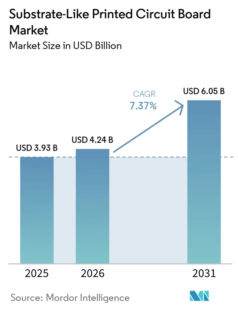
| Market Size (2026) | USD 4.24 Billion |
| Market Size (2031) | USD 6.05 Billion |
| Growth Rate (2026 - 2031) | 7.37% CAGR |
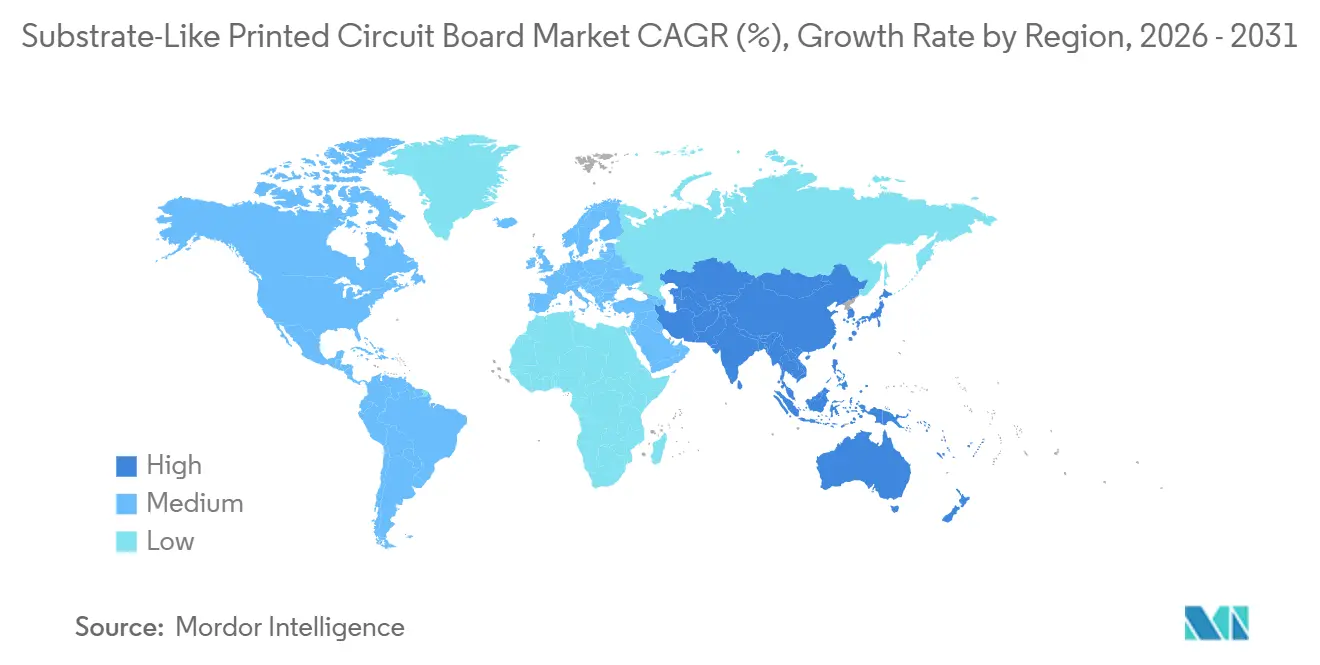
| Fastest Growing Market | Asia Pacific |
| Largest Market | Asia Pacific |
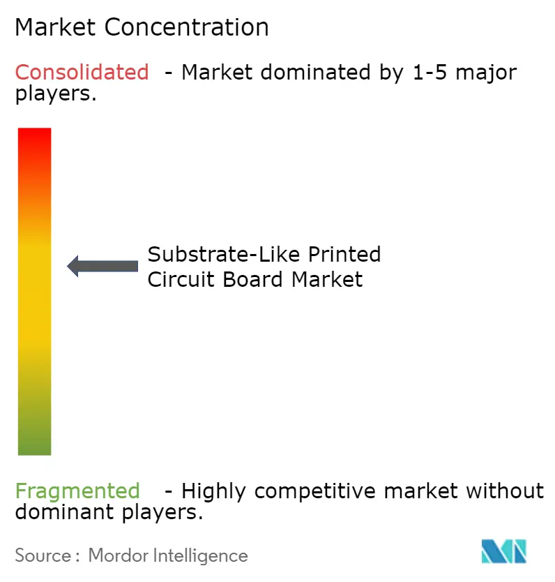
| Market Concentration | Medium |
Major Players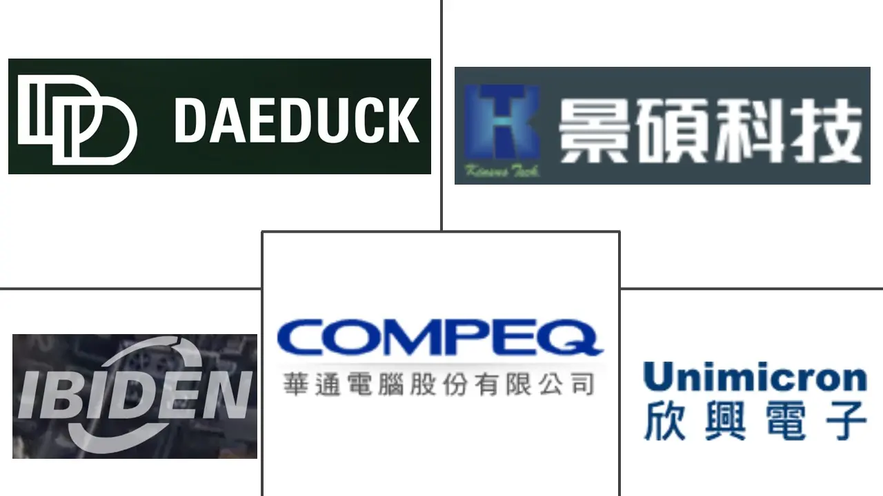 *Disclaimer: Major Players sorted in no particular order Image © Mordor Intelligence. Reuse requires attribution under CC BY 4.0. | |
Substrate-Like Printed Circuit Board Market Analysis by Mordor Intelligence
The Substrate-Like Printed Circuit Board Market size in 2026 is estimated at USD 4.24 billion, growing from 2025 value of USD 3.93 billion with projections showing USD 6.05 billion, growing at 7.37% CAGR over 2026-2031. Momentum stems from demand for line-and-space geometries under 25 µm that bridge the cost gap between traditional printed-wiring boards and full IC substrates. Smartphone makers, 5G infrastructure builders, and automotive electronics integrators are the largest adopters, leveraging higher routing density to shrink form factors, reduce weight, and improve power integrity. At the same time, heterogeneous system-in-package designs that disperse chiplets across a single build-up laminate are redefining substrate value, steering capital toward sequential lamination, laser direct imaging, and automated optical inspection. Supply risk tied to Ajinomoto Build-up Film (ABF) resin and stringent European chemical rules add complexity but also open margins for qualified suppliers that can manage compliance and material security.
Key Report Takeaways
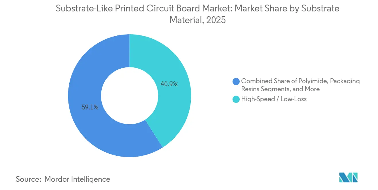
- By substrate material, high-speed and low-loss laminates accounted for 40.94% share of the Substrate-Like PCB market size in 2025 and are expanding at a 7.64% CAGR to 2031.
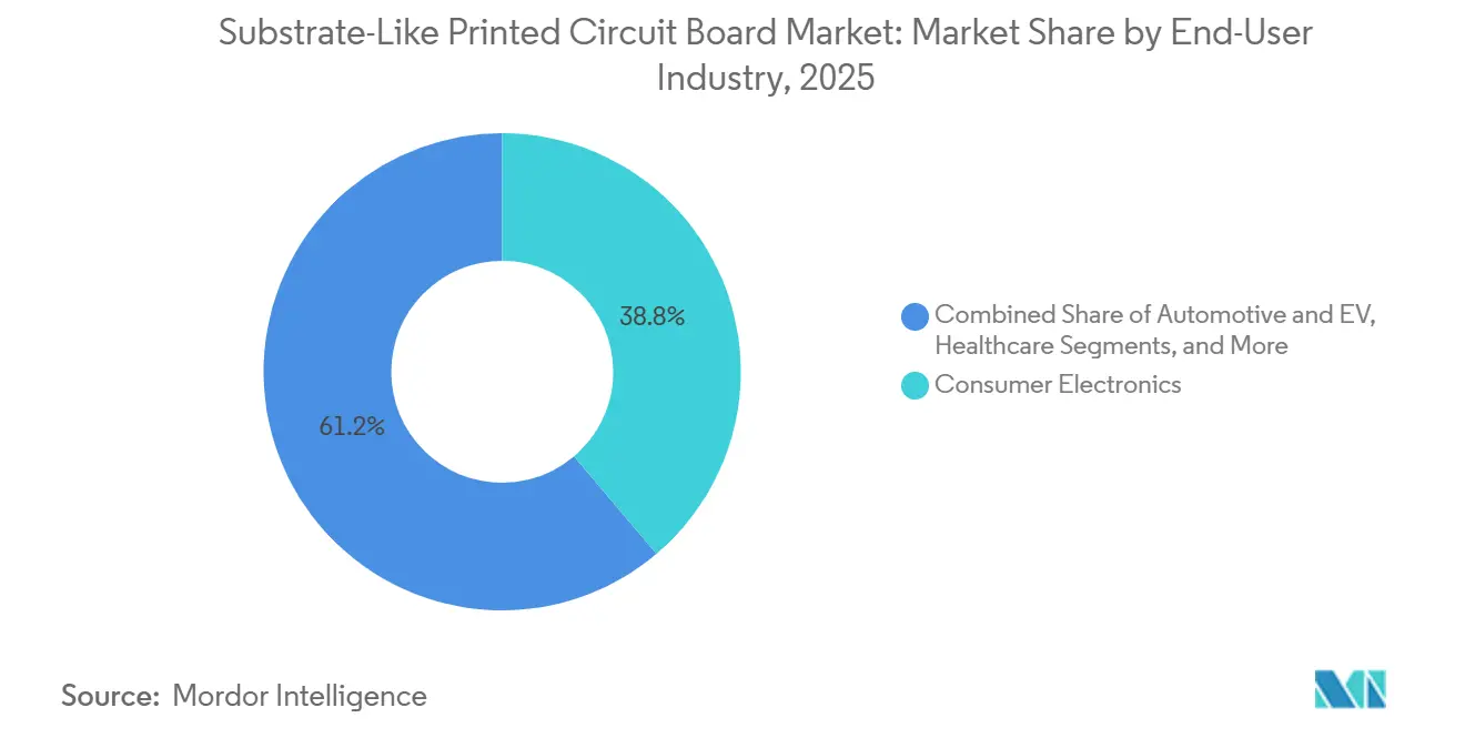
- By end-user industry, telecommunications and 5G recorded the fastest growth at 8.17% CAGR between 2026 and 2031, while consumer electronics retained the largest 38.81% revenue share in 2025.
- By geography, Asia Pacific led with 83.64% of the Substrate-Like PCB market share in 2025; North America and Europe combined posted the highest projected CAGR at 8.77% through 2031.
Note: Market size and forecast figures in this report are generated using Mordor Intelligence’s proprietary estimation framework, updated with the latest available data and insights as of 2026.
Global Substrate-Like Printed Circuit Board Market Trends and Insights
Drivers Impact Analysis*
| Driver | ( ~ ) % Impact on CAGR Forecast | Geographic Relevance | Impact Timeline |
|---|---|---|---|
| Surging Smartphone OEM Adoption for High-Density Interconnects | +1.8% | Global, with concentration in Asia-Pacific (China, Taiwan, South Korea) | Medium term (2-4 years) |
| Rising Demand for 5G Communication Modules | +2.1% | Global, led by North America, Europe, and Asia-Pacific urban centers | Medium term (2-4 years) |
| Miniaturization Trends in Wearables and IoT Devices | +0.9% | Global, with early adoption in North America and Asia-Pacific | Long term (≥ 4 years) |
| Automotive ADAS and EV Electronics Escalating PCB Complexity | +1.5% | Global, strongest in Europe, North America, and China | Long term (≥ 4 years) |
| Flip-Chip on SLP Enabling Heterogeneous Integration | +1.3% | Global, concentrated in Taiwan, South Korea, and Japan | Medium term (2-4 years) |
| Government Subsidies for On-Shore Advanced PCB Fabs | +0.7% | North America, Europe, with selective programs in India and Southeast Asia | Long term (≥ 4 years) |
| Source: Mordor Intelligence | |||
Surging Smartphone OEM Demand for High-Density Interconnects
Smartphone brands have consolidated application processors, RF front ends, and power-management ICs onto single Substrate-Like PCB market boards, cutting occupied area by 30% relative to conventional multilayer designs.[1]Unimicron Technology, “Investor Presentation 2025,” unimicron.com Taiwanese fabricators disclosed that mobile use accounted for over 35% of SLP revenue in 2025, underscoring the volume pull for sub-20 µm lines with via diameters below 50 µm. Yield has become the decisive differentiator as more plants master the geometry, pushing suppliers to couple high-accuracy laser direct imaging with predictive analytics that spot pattern-transfer deviations early.
Rising Demand for 5G Communication Modules
Standalone 5G networks operating at millimeter-wave frequencies impose insertion-loss ceilings of 0.5 dB-in. at 30 GHz that FR-4 can meet only at impractical thicknesses. Base-station OEMs therefore specify high-speed PTFE or liquid-crystal polymer stacks, lifting layer counts beyond eight and driving Substrate-Like PCB market capital spending on automated optical inspection to hold defect escape below 50 PPM.[2]Ericsson, “Annual Report 2025,” ericsson.com Handset makers mirror the trend; dual-band phones integrate multiple power amplifiers and antenna tuners on densified SLP modules, boosting material revenue per device.
Automotive ADAS and EV Electronics Escalating Complexity
Premium electric vehicles embed more than 3,000 cm² of high-reliability boards covering battery management, inverter control and sensor fusion. AEC-Q200 qualification subjects substrate-like printed circuit board market suppliers to 1,000-hour thermal-cycling, damp-heat, and vibration tests, extending development schedules but ensuring failure rates below 15 DPPM in the field AECouncil.com. LiDAR modules require substrates with impedance holding to ±5 Ω at 77-81 GHz, while inverter stages need ceramic-filled laminates dissipating 10 W cm-², steering share toward high-conductivity builds.
Flip-Chip on SLP Enabling Heterogeneous Integration
Mounting bare dies directly on SLP reduces the bill of materials cost by 20-30% by removing the intermediary interposer. Intel, AMD, and NVIDIA attach logic, memory, and analog chiplets to organic build-up substrates that balance coefficient-of-thermal-expansion mismatches using ultra-low-CTE laminates and engineered underfills. Fine-pitch copper redistribution, coupled with over-mold compaction, yields thermal resistance parity with entry IC substrates, widening the addressability of the Substrate-Like PCB market for data-center accelerators.
Restraint Impact Analysis*
| Restraint | ( ~ ) % Impact on CAGR Forecast | Geographic Relevance | Impact Timeline |
|---|---|---|---|
| High CAPEX for SLP Production Lines | -1.2% | Global, particularly acute in North America and Europe | Short term (≤ 2 years) |
| Process-Yield Challenges at 25 µm L/S | -0.9% | Global, most severe in facilities ramping new capacity | Short term (≤ 2 years) |
| Environmental Rules on Specialty Build-Up Chemistries | -0.5% | Europe, with emerging restrictions in North America and Asia-Pacific | Medium term (2-4 years) |
| Supply Risk of ABF Resin Due to Limited Vendors | -1.1% | Global, with Asia-Pacific manufacturers most exposed | Short term (≤ 2 years) |
| Source: Mordor Intelligence | |||
High CAPEX for SLP Production Lines
Greenfield plants capable of 25 µm lines demand USD 150-300 million for laser direct-imaging, sequential lamination and inline X-ray inspection clusters.[3]SEMI, “Capital Equipment Market Report 2025,” semi.org Payback stretches beyond five years unless utilizations exceed 80%, which deters newcomers and consolidates the Substrate-Like PCB market around incumbents that amortize assets across telecom, consumer and automotive contracts.
Supply Risk of ABF Resin Due to Limited Vendors
Ajinomoto and Mitsubishi Gas Chemical earn over 80% of dielectric film revenue, turning component makers into price-takers during demand surges. Kinsus disclosed that ABF constraints limited memory-substrate output in late 2025 and forced premium long-term agreements to secure allocation. Alternate resins remain unproven at dielectrics below 3.5 and Tg above 170 °C, leaving substrate-like printed circuit board market participants exposed until broader qualification achieves customer sign-off.
*Our forecasts treat driver/restraint impacts as directional, not additive. The impact forecasts reflect baseline growth, mix effects, and variable interactions.
Segment Analysis
By Substrate Material: High-Speed Laminates Command the Performance Premium
High-speed and low-loss laminates captured 40.94% of substrate-like printed circuit board market share in 2025, expanding at a 7.64% CAGR through 2031 as PTFE, liquid-crystal polymer, and hydrocarbon-ceramic systems replace glass-epoxy in 5G radio heads and 400-GbE switch fabrics. Insertion loss stays under 0.5 dB-in. at 10 GHz, even as routing lengths shrink, enabling spectral efficiency gains that directly convert into carrier capacity. Glass-epoxy FR-4 still prevails in mid-range smartphones and industrial controls because its raw sheet cost is one-third that of PTFE composites. However, its Substrate-Like PCB market size has begun to taper as handset OEMs chase tighter tolerances for stacked camera arrays.
High-speed materials also spread to data-center accelerator boards, where 112 Gbps PAM4 signaling raises eye-diagram closure sensitivity. Suppliers have started blending hydrocarbon ceramics into ABF resin to lift the glass-transition temperature without sacrificing the dielectric constant. Polyimide retains a niche for flex-rigid builds in automotive and avionics, but share stays below 10% because laser-drilling time and chemistry handling raise process cost. Metal-core and ceramic-filled builds win socket-level power electronics when heat flux exceeds 10 W cm-², a micro-segment that offers high margins but modest volume.


By End-User Industry: Telecommunications Takes the Growth Crown
Telecommunications and 5G rose 8.17% annually and are set to outpace every vertical through 2031 as operators deploy massive-MIMO macro cells and cloud-native core networks. Radio-unit boards integrating beam-forming ICs, power amplifiers, and envelope trackers require eight or more layers fabricated on low-loss stacks, feeding the Substrate-Like PCB market demand for high-bandwidth dielectrics. Consumer electronics still accounted for the largest 38.81% share in 2025, led by smartphones that integrate sub-6 GHz and millimeter-wave antennas.
Computing and data-center use ranks second by revenue, driven by AI accelerators that reach 800-GbE switch backplanes and require signal integrity across one-meter mezzanine links. Automakers continue to multiply board content as EV battery systems, power-inverter modules, and ADAS controllers converge onto zonal architectures, adding 2-3 m² of substrate-like printed circuit board market capacity per premium vehicle. Industrial drives, renewable-energy inverters and medical instruments form smaller but reliability-critical pockets, with ISO 13485 traceability limiting their supply base yet offering premium pricing to qualified fabricators.
Geography Analysis
Asia-Pacific accounted for 83.64% of the Substrate-Like Printed Circuit Board market revenue in 2025, led by Taiwan, China, South Korea, and Japan. Taiwan recorded USD 20.5 billion PCB output in Q3-2024, reflecting an ecosystem of build-up laminate suppliers, laser-equipment firms, and design houses that can prototype within days. Mainland China advances domestic capacity to escape geopolitically fraught imports, with Shennan Circuits expanding ABF lines under state subsidies SCC. South Korea’s conglomerates leverage auto-qualified verticals to enter the EV module market, while Japan maintains process leadership in ultra-thin glass cores. Overall regional growth is projected at 8.77% through 2031, fueled by 5G densification, cloud data-center builds, and EV battery-pack localization
North America and Europe together hold under 15% of the market, constrained by higher labor costs and a thinner material supply chain. The 2022 CHIPS and Science Act earmarked USD 39 billion for semiconductors but excluded substrate facilities from investment tax credits, muting near-term reshoring momentum. A few greenfield pilots, including one in New York and another in Austria, remain in site-selection stages as of early 2026. Rest-of-world demand arises mainly from consumer-electronics final assembly in Southeast Asia and automotive cable-harness plants in Mexico, yet local substrate capacity is negligible, so imports from Taiwan and South Korea dominate.
Geopolitical risk is steering multinational OEMs toward dual-sourcing. Unimicron’s plant in Thailand entered mass production in 2025, offering duty-free access to Association of Southeast Asian Nations markets while dampening cross-strait exposure. European automakers, wary of Taiwanese earthquake disruptions, have entered multi-year sourcing pacts with Korean and Japanese suppliers to secure Substrate-Like Printed Circuit Board market continuity for 800-V battery packs.

Competitive Landscape
The top five suppliers, Unimicron Technology, Ibiden, Kinsus Interconnect Technology, Samsung Electro-Mechanics, and LG Innotek, held a considerable share of the substrate-like printed circuit board market capacity in 2025. Despite this concentration, niches such as polyimide flex-rigid and glass-core substrates remain fragmented due to qualification barriers, substrate warpage, and varying laser-etch innovations. Unimicron’s Thailand site, commissioned in late 2025, adds 6 million ABF panels per month and positions the firm to capture handset booms in Vietnam and Malaysia.
LG Innotek opened its Dream Factory in April 2025 with autonomous material handling and inline machine-learning defect detection, pushing yield above 95% for flip-chip BGA substrates. Kinsus committed USD 101 million to lift ABF output, yet resin allocation remains the bottleneck as memory and accelerator customers consume almost all incremental film. Ibiden is retrofitting its Ogaki lines with sequential lamination ovens to transition from 30 µm to 20 µm lines by 2027.
Emerging Chinese players, buoyed by provincial subsidies, undercut prices in commodity consumer segments but still face long automotive and aerospace qualification cycles. Tier-1 customers increasingly stipulate IPC-6012 Class 3 and real-time traceability, narrowing the vendor list to those with digitized factories and robust cyber-security postures. Patent fences on ABF formulations, laser-drill parameters and photo-resist chemistries further protect incumbents.
Substrate-Like Printed Circuit Board Industry Leaders
Kinsus Interconnect Technology Corp
Ibiden Co., Ltd.
Compeq Manufacturing Co., Ltd.
Daeduck Electronics Co., Ltd.
Unimicron Technology Corp.
- *Disclaimer: Major Players sorted in no particular order

Recent Industry Developments
- January 2026: LG Innotek reported first customer shipments of its carbon-reduced smart IC substrate to a South Korean smartphone OEM, marking commercial adoption two months after pilot production.
- December 2025: LG Innotek began mass production of a smart IC substrate that eliminates precious metals and lowers carbon output by 50% versus prior generations.
- December 2025: Unimicron spun off its flexible-PCB arm and leased the Dajia plant to Uniflex to concentrate capital on IC substrates for AI accelerators.
- December 2025: Kinsus warned of fiberglass cloth and BT substrate tightness amid the memory super-cycle, prompting multiyear supply pacts.
- August 2025: Kinsus allotted USD 101 million to lift ABF substrate capacity at Yangmei Plant 6, aiming for 50 million units monthly by 2027.


Research Methodology Framework and Report Scope
Market Definitions and Key Coverage
According to Mordor Intelligence, our study defines the Substrate-Like Printed Circuit Board (SLP) market as all newly manufactured rigid boards with copper line and space below 30 um, produced through modified semi-additive processes that deliver IC-substrate-level density for smartphones, tablets, wearables, automotive radar modules, networking gear, and advanced industrial controls.
Scope Exclusions: We exclude flexible circuits, ceramic or organic IC package substrates, and conventional HDI boards that use wider trace geometries.
Segmentation Overview
- By Substrate Material
- Glass Epoxy (FR-4)
- High-Speed / Low-Loss
- Polyimide (PI)
- Other Substrate Materials
- By End-user Industry
- Consumer Electronics
- Computing and Data Centers
- Telecommunications and 5G
- Automotive and EV
- Healthcare / Medical
- Aerospace and Defense
- Other End-user Industries
- By Geography
- North America
- United States
- Rest of North America
- Europe
- Germany
- United Kingdom
- Netherlands
- Rest of Europe
- Asia-Pacific
- China
- Taiwan
- Japan
- India
- South Korea
- Southeast Asia
- Rest of Asia-Pacific
- Rest of World
- North America
Detailed Research Methodology and Data Validation
Primary Research
To extend and verify desk findings, we spoke with fabrication managers, materials chemists, smartphone design engineers, and electronics distributors across Asia-Pacific, North America, and Europe. These discussions clarified layer-count adoption paths, feasible yield ramps, and real-world pricing corridors, which then guided sensitivity tests inside the forecast workbook.
Desk Research
In the first stage, our analysts gathered foundational figures from tier-one public sources such as the International Data Corporation smartphone tracker, GSM Association 5Grollout database, WSTS semiconductor shipment tables, UN Comtrade customs statistics, and releases from the Institute of Printed Circuits. Company 10-K filings, investor presentations, and respected press reports were mined to capture average selling price shifts and capacity announcements. Where deeper revenue splits were needed, we referred to licensed repositories from D&B Hoovers and Dow Jones Factiva to cross-check producer footprints. This evidence bank provided the production volumes, device growth outlook, and price benchmarks that seed the model. The sources listed are illustrative only; many additional documents were reviewed for validation and clarification.
Market-Sizing & Forecasting
Our model follows a top-down build that begins with global smartphone, wearable, and automotive electronic unit counts, which are then multiplied by calculated SLP penetration rates drawn from teardown databases, survey feedback, and published design wins. Results are corroborated with selective bottom-up checks; for example, sampling shipment data for key board makers and aligning average selling prices. Core variables include average layers per board, copper-thickness migration, handset replacement cycles, 5Gmix, and regional capacity utilization. Multivariate regression blends these drivers with macro indicators such as semiconductor billings and consumer disposable income to project values through 2030. Where supplier roll-ups diverged from demand pools, analysts applied interview-backed yield adjustments.
Data Validation & Update Cycle
Before release, our Mordor analysts run anomaly scans, compare outputs with independent metrics, and escalate any variance for peer review. The study is refreshed every twelve months, with interim updates triggered by material events like tariff revisions, factory fires, or major capacity additions.
Why Mordor's Substrate-Like PCB Baseline Carries Dependability
We recognize that published estimates often diverge, driven by scope choices, currency bases, and refresh cadence, and because some providers skip on-the-ground checks.
Key gap drivers here include whether flexible and IC package substrates are pooled with SLP, how handset ASP erosion is modeled, and whether China-centric capacity bottlenecks are captured.
Benchmark comparison
| Market Size | Anonymized source | Primary gap driver |
|---|---|---|
| USD 3.53 B (2025) | Mordor Intelligence | |
| USD 12.13 B (2024) | Global Consultancy A | Bundles flexible circuits and IC substrates, applies one global ASP |
| USD 1.50 B (2024) | Industry Publisher B | Uses conservative smartphone penetration and omits automotive and IoT demand |
The comparison shows that while others either broaden or narrow the scope, Mordor's disciplined variable selection, verified price ladders, and annual refresh give decision makers a balanced and traceable benchmark.


Key Questions Answered in the Report
What is the current value of the Substrate-Like PCB market?
The Substrate-Like PCB market size reached USD 3.93 billion in 2025.
How fast will the Substrate-Like PCB market grow through 2031?
Revenue is forecast to increase to USD 6.05 billion by 2031, reflecting a 7.37% CAGR.
Which substrate material leads revenue?
High-speed and low-loss laminates held 40.94% share in 2025 and remain the fastest-growing material group.
Which end-user segment is expanding fastest?
Telecommunications and 5G applications are advancing at an 8.17% CAGR from 2026 to 2031.
Which region dominates production capacity?
Asia-Pacific commanded 83.64% of global Substrate-Like PCB market revenue in 2025 thanks to entrenched ecosystems in Taiwan, China and South Korea.
Page last updated on:


