
SPAD Imaging Sensors For Industrial Vision Market Size and Share
Market Overview
| Study Period | 2020 - 2031 |
|---|---|
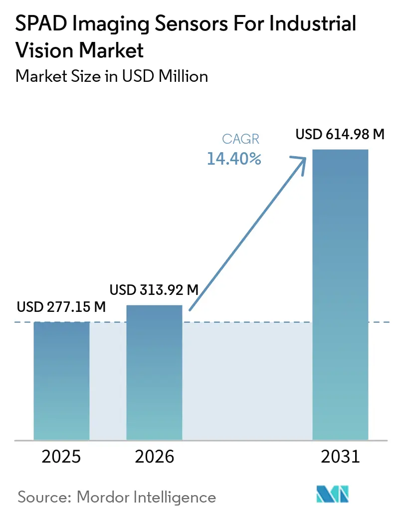
| Market Size (2026) | USD 313.92 Million |
| Market Size (2031) | USD 614.98 Million |
| Growth Rate (2026 - 2031) | 14.40 % |
| Fastest Growing Market | Asia-Pacific |
| Largest Market | Asia-Pacific |
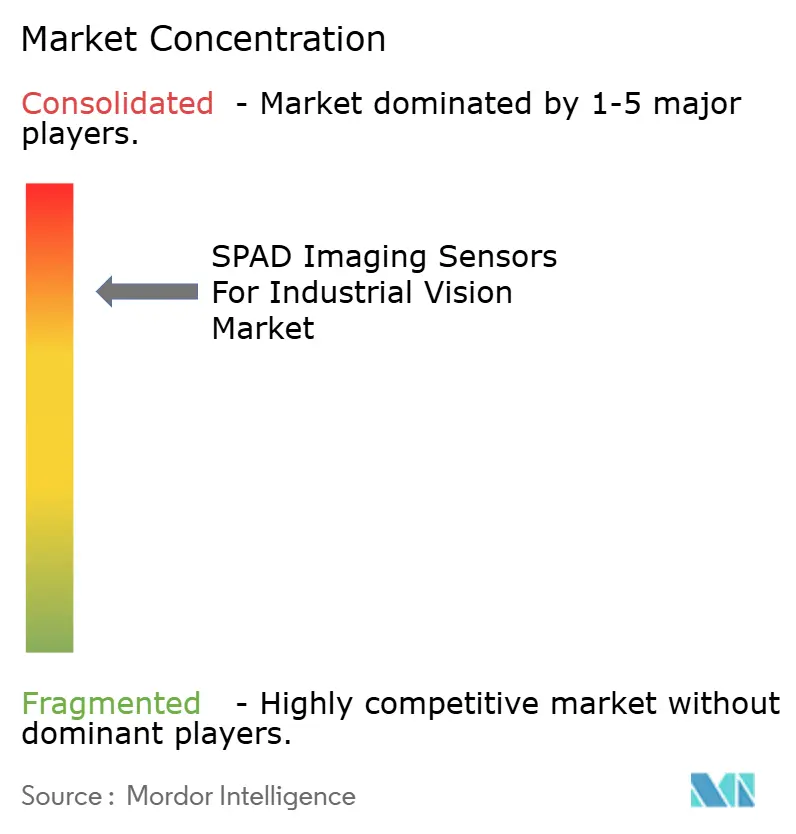
| Market Concentration | High |
Major Players *Disclaimer: Major Players sorted in no particular order Image © Mordor Intelligence. Reuse requires attribution under CC BY 4.0. | |
SPAD Imaging Sensors For Industrial Vision Market Analysis by Mordor Intelligence
The SPAD Imaging Sensors for Industrial Vision Market size was valued at USD 277.15 million in 2025 and is estimated to expand from USD 313.92 million in 2026 to reach USD 614.98 million by 2031, at a CAGR of 14.40% during the forecast period, 2026-2031. Demand is supported by wider use of 3D machine vision in factory automation and logistics, where depth information improves robot guidance and material handling. Inspection requirements in semiconductor packaging also favor photon-counting sensors because they can capture weak signals at high operating speeds. Direct time-of-flight sensing is becoming increasingly relevant for autonomous mobile robots that require reliable ranging in changing lighting conditions. Competition is increasingly centered on stacked-sensor designs, software support, and industrial qualification rather than on pixel performance alone. High process costs, interoperability requirements, sensor noise trade-offs, and a limited specialist talent base will keep adoption focused on applications where performance justifies the investment.
Key Report Takeaways
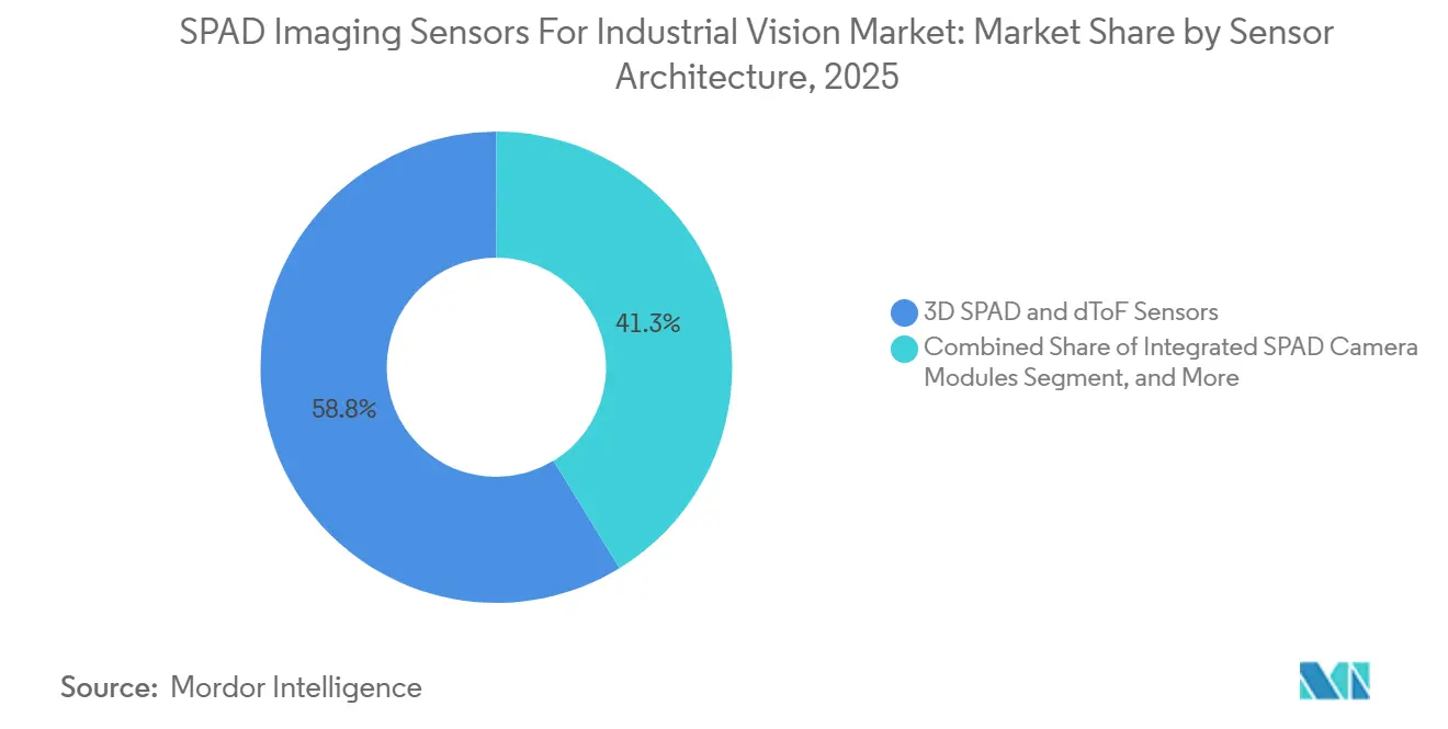
- By sensor architecture, 3D SPAD/dToF sensors held 58.75% market share in 2025, while integrated SPAD camera modules and vision systems are projected to expand at a 21.63% CAGR through 2031.
- By wavelength range, NIR SPAD sensors accounted for 82.35% market share in 2025, while SWIR SPAD sensors are projected to record a 21.47% CAGR through 2031.
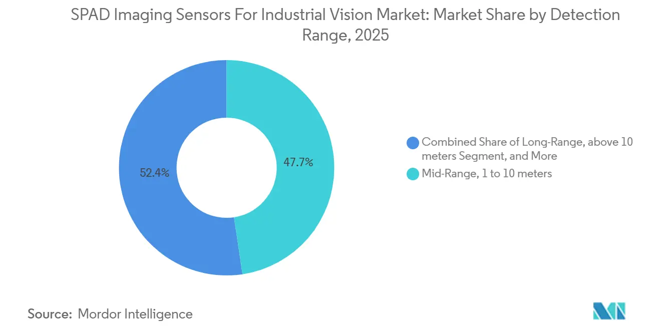
- By detection range, mid-range sensors held a 47.65% share in 2025, while long-range sensors are projected to advance at a 20.85% CAGR through 2031.
- By end-user industry, electronics and semiconductor manufacturers represented 24.85% market share in 2025, while logistics and warehousing are projected to record a 21.74% CAGR through 2031.
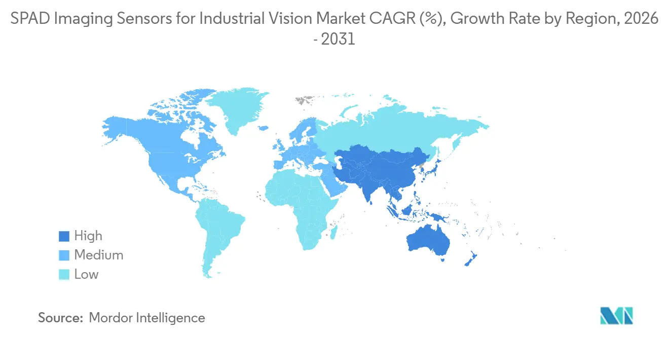
- By geography, Asia-Pacific held 46.75% market share in 2025 and is projected to expand at a 21.36% CAGR through 2031.
Note: Market size and forecast figures in this report are generated using Mordor Intelligence’s proprietary estimation framework, updated with the latest available data and insights as of January 2026.
Global SPAD Imaging Sensors For Industrial Vision Market Trends and Insights
Drivers Impact Analysis*
| Driver | (~) % Impact on CAGR Forecast | Geographic Relevance | Impact Timeline |
|---|---|---|---|
| Expansion of 3D Machine Vision and Robotics | +3.8% | Global, concentrated in Asia-Pacific, Europe, and North America | Medium term (2-4 years) |
| Demand for Low-Light, High-Speed Inspection | +3.2% | Global, with electronics and semiconductor hubs in Asia-Pacific and North America | Short term (≤ 2 years) |
| Growth of Direct Time-of-Flight Ranging | +2.8% | Global, led by Asia-Pacific robotics and North America logistics | Medium term (2-4 years) |
| Rising Adoption of Edge AI in Factory Automation | +2.4% | North America, Europe, and Asia-Pacific | Medium term (2-4 years) |
| Semiconductor-Stacking Advances Lowering Sensor Footprint | +1.8% | Global, with key gains in Japan, Taiwan, and South Korea | Long term (≥ 4 years) |
| Photon-Counting Requirements in Semiconductor and Life-Science Inspection | +1.4% | North America and Europe, with spillover to Asia-Pacific | Short term (≤ 2 years) |
| Source: Mordor Intelligence | |||
Expansion of 3D Machine Vision and Robotics Drives Sensor Adoption
3D machine vision is now used beyond automotive and semiconductor assembly lines in food sorting, pharmaceutical pick-and-pack, logistics automation, and collaborative robotics. In the SPAD Imaging Sensors for Industrial Vision Market, SPAD-based dToF cameras generate depth data from a single laser pulse and can operate independently of ambient light. This makes them different from structured-light and stereo-vision systems, which can require more processing or controlled illumination. RoboSense reported that robotics LiDAR shipments increased 510.4% year over year in H1 2026.[1] supported by its EOCENE SPAD-SoC architecture, and it projected 800,000-1,000,000 robotics LiDAR deliveries for full-year 2026. As image-grade 3D output becomes available at more viable price points, bin picking, gap detection, and volumetric measurement become more practical for the SPAD Imaging Sensors for Industrial Vision Market. Higher autonomous mobile robot fleet density also requires long-range sensing for spacing and emergency-stop coverage across warehouse floors.
Demand for Low-Light, High-Speed Inspection Favors SPAD Architecture
Industrial production lines operate continuously and may run conveyor systems at speeds above 5 meters per second, which increases the need for defect detection without motion blur. For the SPAD Imaging Sensors for Industrial Vision Market, photon-counting operation removes readout noise and supports shorter exposures than conventional CMOS cameras at comparable signal-to-noise performance. Pi Imaging demonstrated its 1,024×1,024-pixel SPAD Alpha camera for industrial machine vision at VISION 2026 and described photon-shot-noise-limited performance for high-speed inspection.[2] The camera also reduces downstream computational demand for edge inference models. The SPAD Imaging Sensors for Industrial Vision Market benefits as inspection shifts from 2D surface checks toward volumetric analysis of subsurface voids in chip packages and delamination in battery electrodes. Time-correlated photon counting can provide depth data and photon-arrival information in one acquisition event.
Growth of Direct Time-of-Flight Ranging Reshapes Depth Sensing Economics
Direct time-of-flight ranging measures the interval between laser emission and photon detection by a SPAD sensor. It is suited to industrial applications that require metric accuracy beyond 1 meter and can reduce reliance on structured-light and phase-shift methods. STMicroelectronics launched the VL53L9 in June 2026, a dToF 3D LiDAR module with 2,268 zones, a range from less than 5 cm to 9 meters, up to 1% accuracy, and operation at 100 frames per second.[3] Its mass production began in July 2026. This supports demand in the SPAD Imaging Sensors for Industrial Vision Market for sensors with strong photon rejection rather than higher laser power. IEC 60825-1 laser safety considerations also favor sensitive designs that operate with Class 1 sources.
Rising Adoption of Edge AI in Factory Automation Amplifies SPAD Value
Local AI inference can reduce the delay between image capture and a production decision, which matters when defective products must be diverted within milliseconds. Cisco identified AI-powered automated guided vehicles and machine vision systems as major investment priorities among manufacturers deploying AI at scale in 2026.[4] Three-dimensional stacked SPAD designs separate the photon-detection layer from the logic wafer, creating space for histogram processors and neural-network accelerators. Singular Photonics launched its Litavis sensor on September 10, 2026, featuring in-pixel processing for imaging, timing, and histogram functions on a single CMOS chip. The company stated that lower raw data transfers and latency support edge AI use in robotics and industrial automation. The SPAD Imaging Sensors for Industrial Vision Market, therefore, places increasing value on sensors that convert photon data into usable device-level decisions.
Restraints Impact Analysis*
| Restraint | (~) % Impact on CAGR Forecast | Geographic Relevance | Impact Timeline |
|---|---|---|---|
| High Pixel-Level Process and Packaging Costs | -3.5% | Global, more acute in North America and Europe | Short term (≤ 2 years) |
| Limited Industrial Qualification and Interoperability | -2.1% | Global | Medium term (2-4 years) |
| Dark-Count, Afterpulsing, and Ambient-Light Trade-Offs | -1.8% | Global, particularly high in outdoor industrial settings | Long term (≥ 4 years) |
| Scarcity of Specialized SPAD Design and Test Talent | -1.2% | North America and Europe primarily | Medium term (2-4 years) |
| Source: Mordor Intelligence | |||
High Pixel-Level Process and Packaging Costs Limit Market Breadth
SPAD sensors require specialized CMOS processes with deep-trench isolation and carefully engineered avalanche junctions. Stacked variants also require wafer-to-wafer or chip-to-chip hybrid bonding, which is not widely available at commodity CMOS foundries. Per-pixel costs are 3-5 times higher than those of mainstream global-shutter CMOS sensors, limiting use in price-sensitive food sorting and mid-volume machine-tending applications. Sony Semiconductor Solutions introduced Cu-Cu bonding in the IMX479 in June 2025 to improve stacking yield and reduce footprint, but a meaningful cost gap remained. This cost pressure encourages early adopters in the SPAD Imaging Sensors for Industrial Vision Market to procure integrated camera modules rather than bare sensors. That approach shifts engineering complexity and margin to system vendors and can reduce flexibility for customers that need custom configurations.
Limited Industrial Qualification and Interoperability Extends Development Cycles
Many commercial SPAD products have certifications designed for automotive or medical uses, rather than for industrial machine vision. Sony's IMX560 lists IEC 61508 SIL 2 readiness, while industrial users may also require GenICam, GigE Vision, USB3 Vision, CoaXPress, temperature, and electromagnetic-compatibility validation. Closing this qualification gap can add 12-18 months to product development cycles. The required test infrastructure also favors established machine-vision providers that have existing qualification programs. A lack of standard histogram data formats makes multisupplier integration harder and requires custom middleware. These conditions raise ownership costs in the SPAD Imaging Sensors for Industrial Vision Market beyond the initial sensor purchase price
*Our forecasts treat driver/restraint impacts as directional, not additive. The impact forecasts reflect baseline growth, mix effects, and variable interactions.
Segment Analysis
By Sensor Architecture: 3D dToF Leads While Integrated Modules Accelerate
3D SPAD/dToF sensors held 58.75% of the SPAD Imaging Sensors for Industrial Vision Market share in 2025. Their position reflects the ability to combine depth, accuracy, and single-photon sensitivity across mid-range operating distances. These sensors support robotic bin picking, autonomous guided vehicle obstacle avoidance, warehouse zone mapping, and factory safety monitoring. Sony's IMX560 industrial dToF SPAD sensor offers IEC 61508 SIL 2 readiness, 100 frames-per-second operation, and a 1 GHz sampling frequency. These specifications show how dToF designs are moving from prototypes to qualified products for safety-related industrial uses.
Integrated SPAD camera modules and vision systems are projected to record a 21.63% CAGR from 2026 to 2031. In the SPAD Imaging Sensors for Industrial Vision Market, system integrators use pre-calibrated and firmware-managed products to shorten deployment schedules. This model transfers more integration work to the module supplier. Linear SPAD sensors continue to support web inspection, wafer-edge scanning, and roll-to-roll material monitoring. Two-dimensional area-scan SPAD sensors are used for time-resolved fluorescence inspection in pharmaceutical and life-science settings, where photon-arrival statistics are as important as image intensity.

By Wavelength Range: NIR Holds the Largest Position While SWIR Gains Use Cases
NIR SPAD sensors in the 700-1,100 nm range accounted for 82.35% market share in 2025. Silicon SPAD devices provide strong photon-detection performance at 905 nm and 940 nm. These wavelengths are common in industrial vertical-cavity surface-emitting laser illuminators because they support cost control and Class 1 eye-safety requirements. Hamamatsu's C16531 series has photon detection efficiency up to 65% at 630 nm and extends to 1,000 nm. This coverage supports reflectance inspection, dToF ranging, and agricultural sorting.
SWIR SPAD sensors are projected to advance at a 21.47% CAGR from 2026 to 2031. For the SPAD Imaging Sensors for Industrial Vision Market, room-temperature InGaAs/InP and Ge-on-Si platforms make 1,100-1,700 nm detection possible without cryogenic cooling. A 3D-stacked InGaAs/InP sensor presented at CLEO 2026 delivered outdoor depth imaging at 10 meters under 120,000 lux sunlight with 2% accuracy. This result supports use in outdoor industrial settings with strong ambient light. Ultraviolet-to-visible SPADs remain relevant for semiconductor critical-dimension metrology, while extended SWIR devices above 1,700 nm remain in an early research stage due to material and thermal-management requirements.
By Detection Range: Mid-Range Systems Form the Largest Base While Long-Range Demand Builds
Mid-range sensors covering 1-10 meters accounted for 47.65% of the market in 2025. The range fits common factory layouts, including 1-3-meter robotic-arm reach, 2-6-meter conveyor monitoring, and 5-8-meter automated guided vehicle navigation. STMicroelectronics' VL53L9 provides 2,268 zones across distances from less than 5 cm to 9 meters in a 12.8 mm × 6.1 mm package. This product illustrates the current performance level of the mid-range category. It also links compact form factors with the depth requirements of industrial automation.
Long-range sensors over 10 meters are projected to grow at a 20.85% CAGR through 2031. In the SPAD Imaging Sensors for Industrial Vision Market, warehouse perimeter monitoring, outdoor automated guided vehicle yards, and high-bay storage systems require sensing ranges of 20-50 meters. Advances in 3D-stacked back-side-illuminated SPAD timing circuits support this use case. An equivalent-time sampling design reported by the ITE Symposium delivered 25 million points per second in an automotive-grade sensor concept that can inform industrial outdoor designs. Short-range products up to 1 meter remain appropriate for gesture recognition, proximity switching, and component-presence checks. Their use is constrained by lower-cost time-of-flight and ultrasonic alternatives.
By End-User Industry: Semiconductor Inspection Leads While Logistics and Warehousing Expands
Electronics and semiconductor manufacturers accounted for 24.85% of the SPAD Imaging Sensors for Industrial Vision Market size in 2025. Photon-counting systems identify defects in flip-chip micro-bumps, 3D-IC stacks, and through-silicon vias that can fall below the signal-to-noise limit of conventional cameras. The IPC-A-610 standard sets strict requirements for solder joint and wire bond quality. These requirements reinforce the case for sensitive inspection tools as chip structures become denser. The segment also depends on suppliers' ability to deliver repeatable results in demanding packaging workflows.
Logistics and warehousing are projected to advance at a 21.74% CAGR from 2026 to 2031. Across the SPAD Imaging Sensors for Industrial Vision Market, e-commerce fulfillment operations use SPAD dToF sensors in autonomous mobile robots for carton measurement, goods identification under varied illumination, and dock-door sensing. RoboSense reported a 1,458.8% year-over-year increase in robotics LiDAR shipments in Q1 2026. Automotive and mobility users seek long-range, high-angular-resolution LiDAR. At the same time, machinery and robotics buyers need mid-range dToF modules for collaborative robot safety. Pharmaceutical and medical equipment makers use UV-to-NIR products for particle counting and fluorescence lifetime inspection. In contrast, food and beverage operators use NIR products for foreign-material sorting. Aerospace and defense users are evaluating SWIR SPAD systems for low-light ranging.
Geography Analysis
Asia-Pacific held 46.75% of the SPAD Imaging Sensors for Industrial Vision Market share in 2025 and is projected to record a 21.36% CAGR through 2031. China is both the largest regional consumer and an increasingly capable producer of SPAD sensors. PolarisIC launched the PCM7200 in September 2026, China's first commercial 3.2-megapixel SPAD image sensor, using a second-generation 3D-stacked back-side-illuminated design with an 8 μm pixel pitch and a 2,080×1,568 array. Japan retains a strong position in stacked process technology and automotive-grade depth sensing. South Korea's semiconductor and display production base sustains demand for high-line-rate inspection systems, while China's smart-manufacturing programs place SPAD procurement within factory modernization plans.
In the SPAD Imaging Sensors for Industrial Vision Market, North America is shaped by semiconductor fabs, pharmaceutical equipment suppliers, and defense-related inspection programs where photon-counting performance can support premium pricing. Excelitas offers the SPCM-1064 single-photon counting module with photon detection efficiency above 70% at 650 nm and coverage to 1,064 nm for precision measurement and quantum optics uses. Europe combines a precision machine-vision base with academic and industrial collaboration in SPAD development. Singular Photonics launched Litavis in Edinburgh in September 2026, while STMicroelectronics began mass production of the VL53L9 in July 2026 for worldwide distribution. The EU Chips Act is expected to support the development of the photonic and semiconductor supply chains through research partnerships and capacity investments.
South America and Middle East, and Africa remain early-stage regions for the SPAD Imaging Sensors for Industrial Vision Market. In South America, automotive assembly and agribusiness inspection lines are key near-term settings for surface-defect detection and agricultural sorting. Middle East industrial diversification programs in Saudi Arabia and the United Arab Emirates include logistics infrastructure and manufacturing parks that can support the deployment of sensor-intensive autonomous mobile robots. South Africa's mining and mineral-processing sector is the main current African application area, and both regions are likely to access SPAD technology through global original equipment manufacturer system integrators before domestic procurement channels mature.
Competitive Landscape
The SPAD Imaging Sensors for Industrial Vision Market has moderate concentration among leading suppliers. Sony Semiconductor Solutions, Hamamatsu Photonics, STMicroelectronics, and ams-OSRAM hold positions through proprietary processes, stacked architectures, and established industrial and automotive qualification programs. Their advantage includes calibration software, reference designs, application engineering, and customer qualification support. These capabilities can reduce integration risk for original equipment manufacturer buyers. System integration is an important source of competitive protection, not merely individual pixel performance.
Chinese fabless suppliers, including PolarisIC, Adaps Photonics, and visionICs, are applying price pressure in dToF and area-scan products through domestic foundry access and supply-chain depth. PolarisIC's PCM7200 launch marked a move toward commercial megapixel-class SPAD imaging. At the high end, STMicroelectronics combines its VL53L9 sensor, metasurface optics, and dToF processing in a calibration-free module intended for edge-AI systems. This strategy extends value beyond the sensor die and makes software and integration part of the product offer. At the mid-market level, Adaps Photonics uses back-side-illuminated SPAD arrays hybrid-bonded to custom digital signal processing dies for robotics and industrial depth sensing.
Room-temperature SWIR arrays for food and pharmaceutical inspection remain an open product area because no industrially qualified, high-resolution product is currently available. Sony improved its stacking approach with Cu-Cu bonding in the IMX479, while Singular Photonics incorporated in-pixel processing into its Litavis design. STMicroelectronics began mass production of a compact dToF module that integrates sensing and processing. These actions show that the SPAD Imaging Sensors for Industrial Vision Market is competing by leveraging stacked architectures, reduced integration, and device-level processing.
SPAD Imaging Sensors For Industrial Vision Industry Leaders
-
STMicroelectronics N.V.
-
ams-OSRAM AG
-
Sony Semiconductor Solutions Corporation
-
Hamamatsu Photonics K.K.
-
Canon Inc.
- *Disclaimer: Major Players sorted in no particular order
Recent Industry Developments
- September 2026: Singular Photonics launched Litavis, the world's first SPAD sensor using in-pixel processing to unify imaging, timing, histogramming, and photon statistics on a single CMOS chip. The sensor delivers 47% photon detection efficiency at 785 nm and 37 ps timing resolution; the company reported significant global pre-order volumes from manufacturing and research customers at launch, targeting machine vision, robotics, and industrial automation deployments.
- September 2026: PolarisIC launched the PCM7200, China's first commercial 3.2-megapixel SPAD image sensor, featuring a 2080×1568 array on a second-generation 3D-stacked BSI architecture with an 8 μm pixel pitch, the largest SPAD imaging array commercially available at this time. The sensor's TunRes tunable-response pixel technology addresses power-consumption and high-dynamic-range challenges in large-area SPAD imaging, directly filling a domestic supply gap.
- August 2026: RoboSense reported robotics LiDAR shipments rising 510.4% year over year in H1 2026, driven by its EOCENE SPAD-SoC architecture and the associated Phoenix and Peacock chipsets targeting industrial automation, logistics, and autonomous driving applications; the company projected full-year 2026 total LiDAR deliveries of 2-2.7 million units.
- June 2026: STMicroelectronics launched the ST FlightSense VL53L9, a compact dToF 3D LiDAR all-in-one module using stacked BSI SPAD technology, delivering 2,268 resolution zones and ranging from less than 5 cm to 9 meters with 1% accuracy at 100 frames per second; mass production commenced in July 2026 for global distribution across robotics, industrial automation, and smart-building markets.
Global SPAD Imaging Sensors For Industrial Vision Market Report Scope
SPAD Image Sensors are advanced single-photon detection devices that utilize avalanche photodiodes operating in Geiger mode to capture extremely low-light signals and precise time-of-flight data, enabling high-sensitivity 3D imaging, depth mapping, and ultra-fast timing applications in industrial and scientific environments.
The SPAD Image Sensors Market Report is Segmented by Sensor Architecture (Linear (Line-Scan) SPAD Sensors, 2D (Area-Scan) SPAD Image Sensors, 3D SPAD / dToF Sensors, and Integrated SPAD Camera Modules and Vision Systems), Wavelength Range (Ultraviolet to Visible (Less than 700 nm), Near-Infrared (700 - 1,100 nm), Short-Wave Infrared (1,100 - 1,700 nm), and Extended SWIR (More than 1,700 nm)), Detection Range (Short-Range, up to 1 meter, Mid-Range, 1 to 10 meters, and Long-Range, above 10 meters), End-User Industry (Automotive and Mobility, Electronics and Semiconductor, Food and Beverage, Pharmaceutical and Medical Equipment, Machinery and Robotics, Logistics and Warehousing, Aerospace and Defense, and Other End-User Industries), and Geography (North America, South America, Europe, Asia-Pacific, Middle East and Africa). The Market Forecasts are Provided in Terms of Value (USD).
| Linear (Line-Scan) SPAD Sensors |
| 2D (Area-Scan) SPAD Image Sensors |
| 3D SPAD / dToF Sensors |
| Integrated SPAD Camera Modules and Vision Systems |
| Ultraviolet to Visible (Less than 700 nm) |
| Near-Infrared (700 - 1,100 nm) |
| Short-Wave Infrared (1,100 - 1,700 nm) |
| Extended SWIR (More than 1,700 nm) |
| Short-Range, up to 1 meter |
| Mid-Range, 1 to 10 meters |
| Long-Range, above 10 meters |
| Automotive and Mobility |
| Electronics and Semiconductor |
| Food and Beverage |
| Pharmaceutical and Medical Equipment |
| Machinery and Robotics |
| Logistics and Warehousing |
| Aerospace and Defense |
| Other End-User Industries |
| North America | United States | |
| Canada | ||
| Mexico | ||
| South America | Brazil | |
| Argentina | ||
| Rest of South America | ||
| Europe | Germany | |
| United Kingdom | ||
| France | ||
| Italy | ||
| Spain | ||
| Rest of Europe | ||
| Asia-Pacific | China | |
| Japan | ||
| India | ||
| South Korea | ||
| Rest of Asia-Pacific | ||
| Middle East and Africa | Middle East | Saudi Arabia |
| United Arab Emirates | ||
| Turkey | ||
| Rest of the Middle East | ||
| Africa | South Africa | |
| Nigeria | ||
| Rest of Africa | ||
| By Sensor Architecture | Linear (Line-Scan) SPAD Sensors | ||
| 2D (Area-Scan) SPAD Image Sensors | |||
| 3D SPAD / dToF Sensors | |||
| Integrated SPAD Camera Modules and Vision Systems | |||
| By Wavelength Range | Ultraviolet to Visible (Less than 700 nm) | ||
| Near-Infrared (700 - 1,100 nm) | |||
| Short-Wave Infrared (1,100 - 1,700 nm) | |||
| Extended SWIR (More than 1,700 nm) | |||
| By Detection Range | Short-Range, up to 1 meter | ||
| Mid-Range, 1 to 10 meters | |||
| Long-Range, above 10 meters | |||
| By End-User Industry | Automotive and Mobility | ||
| Electronics and Semiconductor | |||
| Food and Beverage | |||
| Pharmaceutical and Medical Equipment | |||
| Machinery and Robotics | |||
| Logistics and Warehousing | |||
| Aerospace and Defense | |||
| Other End-User Industries | |||
| By Geography | North America | United States | |
| Canada | |||
| Mexico | |||
| South America | Brazil | ||
| Argentina | |||
| Rest of South America | |||
| Europe | Germany | ||
| United Kingdom | |||
| France | |||
| Italy | |||
| Spain | |||
| Rest of Europe | |||
| Asia-Pacific | China | ||
| Japan | |||
| India | |||
| South Korea | |||
| Rest of Asia-Pacific | |||
| Middle East and Africa | Middle East | Saudi Arabia | |
| United Arab Emirates | |||
| Turkey | |||
| Rest of the Middle East | |||
| Africa | South Africa | ||
| Nigeria | |||
| Rest of Africa | |||
Key Questions Answered in the Report
What is the size of the SPAD Imaging Sensors for Industrial Vision Market?
The SPAD Imaging Sensors for Industrial Vision Market was valued at USD 277.15 million in 2025 and is estimated at USD 313.92 million in 2026. It is projected to reach USD 614.98 million by 2031 at a 14.40% CAGR. Factory automation, logistics, and semiconductor inspection support this outlook.
Which sensor architecture has the largest share?
3D SPAD/dToF sensors held 58.75% share in 2025, supported by industrial depth sensing, robot guidance, and safety monitoring.
Which wavelength range is expanding fastest?
SWIR SPAD sensors are projected to record a 21.47% CAGR through 2031 as room-temperature platforms extend sensing into the 1,100-1,700 nm range.
Why do industrial users select SPAD sensors?
SPAD sensors support low-light imaging, fast inspection, photon counting, and direct time-of-flight depth measurement for complex factory applications.
Which end-user sector is expanding fastest?
Logistics and warehousing is projected to advance at a 21.74% CAGR through 2031 as autonomous mobile robots need carton measurement, navigation, and dock-door sensing.
Which region is expected to lead expansion?
Asia-Pacific held 46.75% share in 2025 and is projected to record a 21.36% CAGR through 2031, supported by China, Japan, and South Korea.