Semiconductor Lithography Equipment Market Size
Market Overview
| Study Period | 2019 - 2030 |
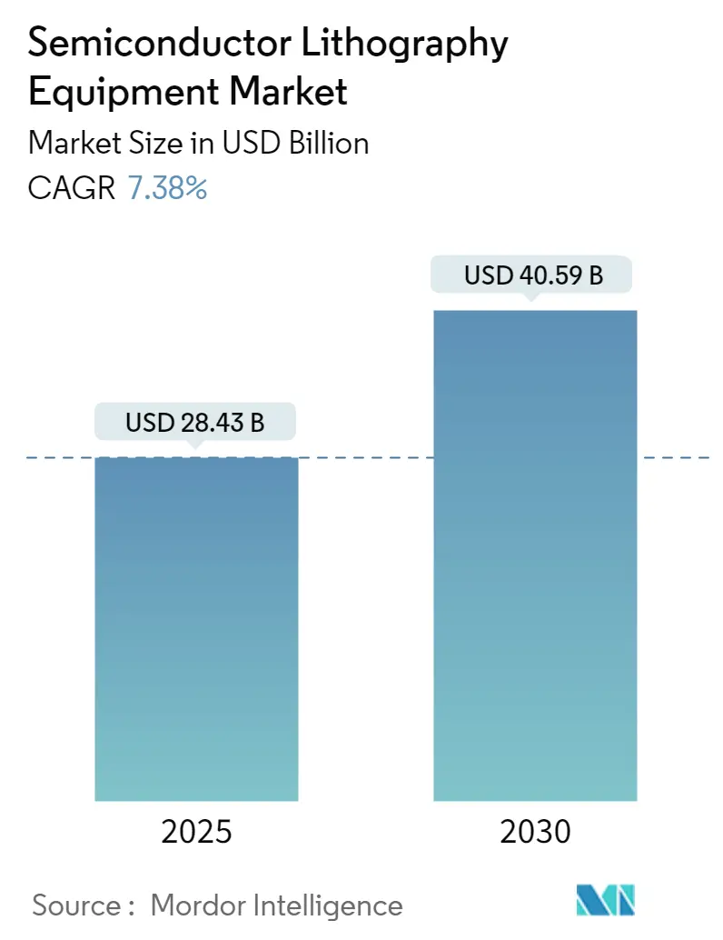
| Market Size (2025) | USD 28.43 Billion |
| Market Size (2030) | USD 40.59 Billion |
| Growth Rate (2025 - 2030) | 7.38% CAGR |
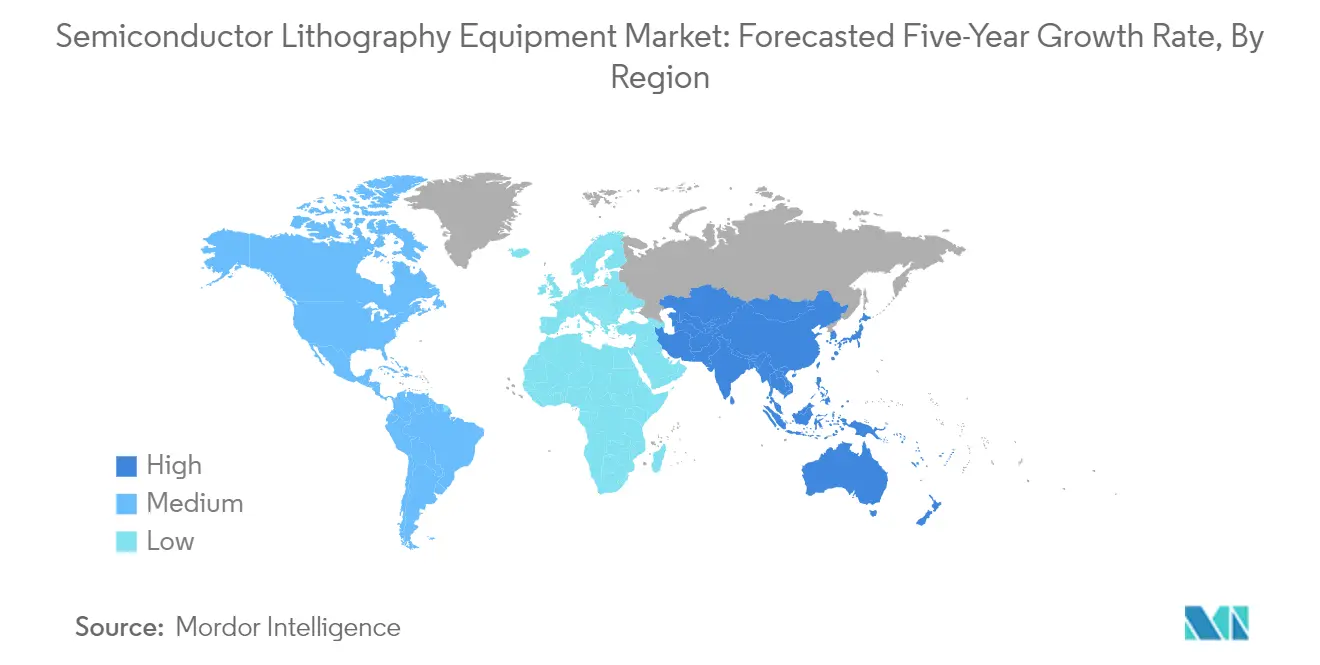
| Fastest Growing Market | Asia Pacific |
| Largest Market | Asia Pacific |
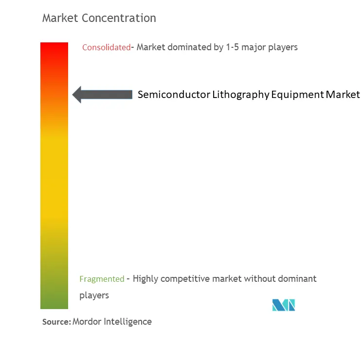
| Market Concentration | High |
Major Players*Disclaimer: Major Players sorted in no particular order Image © Mordor Intelligence. Reuse requires attribution under CC BY 4.0. |
|
Semiconductor Lithography Equipment Market Analysis
The Semiconductor Lithography Equipment Market size is estimated at USD 28.43 billion in 2025, and is expected to reach USD 40.59 billion by 2030, at a CAGR of 7.38% during the forecast period (2025-2030).
The semiconductor lithography equipment industry operates within a highly complex manufacturing ecosystem, characterized by intricate production processes and technological precision requirements. The manufacturing process involves approximately 1,400 distinct steps in the complete production and inspection of semiconductor wafers, highlighting the sophisticated nature of the industry. Semiconductor manufacturing equipment and tools constitute more than 50% of semiconductor fabrication costs, emphasizing the critical role of lithography systems in the overall semiconductor manufacturing process. This complexity has led to an increased focus on precision engineering and quality control measures, as manufacturers strive to maintain high yields while managing the intricate nature of semiconductor fabrication.
The industry is experiencing a significant transformation driven by the rapid evolution of communication technologies and digital connectivity. According to GSMA, 5G mobile broadband connections are expected to reach 1,100 million by 2025, with the 5G rollout anticipated to cover 34% of the world's population by the same year. This technological advancement is reshaping the semiconductor manufacturing landscape, as semiconductor lithography equipment manufacturers adapt their systems to meet the demanding requirements of next-generation semiconductor devices. The integration of advanced connectivity features in modern devices has created a surge in demand for more sophisticated lithography solutions capable of producing increasingly complex semiconductor components.
The market is witnessing substantial technological advancements in lithography equipment capabilities. In March 2022, Nikon Corporation launched a new Gen 8 plate FPD lithography system to support the production of various high-definition panels for value-added premium displays, demonstrating the industry's commitment to innovation. Equipment manufacturers are focusing on developing systems that can handle more intricate pattern designs and smaller node sizes, while simultaneously improving throughput and reducing defect rates. This evolution in semiconductor process equipment capabilities is essential to meet the growing demand for advanced semiconductor devices across various applications.
The industry landscape is being reshaped by strategic investments and facility expansions by major equipment manufacturers. Canon's announcement of a new semiconductor equipment plant in eastern Japan, scheduled to commence operations in 2025, exemplifies the industry's focus on expanding production capabilities. Similarly, ASML's development of next-generation extreme ultraviolet lithography machines, capable of producing microchips with unprecedented precision, showcases the industry's commitment to pushing technological boundaries. These developments are crucial in addressing the growing demand for advanced semiconductor devices while ensuring the industry can meet future technological challenges. The introduction of advanced wafer processing equipment and chip manufacturing equipment is pivotal in supporting these technological advancements.
Semiconductor Lithography Equipment Market Trends
Increasing Demand for Miniaturization and Extra Functionality by Electric Vehicles and Advanced Mobile Devices
Electronic components in the automotive industry are becoming increasingly critical for safety and are subjected to extreme voltages and environmental conditions, driving about 80% of today's automotive innovation. Applications in intelligence, connectivity, sensing, and control are evolving to keep pace with the growing complexity of safer, greener, and smarter vehicle design. The increasing adoption of advanced features in EVs, such as high-resolution intelligent displays, park-assist cameras, touchscreens, automatic wipers and lights, 30-minute rapid charging capability, and eco-friendly components, has been driving the demand for semiconductor manufacturing equipment. These requirements necessitate more sophisticated semiconductor lithography equipment capable of producing smaller, more efficient chips while maintaining high performance and reliability.
The miniaturization trend in mobile devices and consumer electronics continues to push the boundaries of semiconductor manufacturing capabilities. According to industry data, the connected devices running on semiconductor chips (IoT devices) market is projected to reach USD 75 billion by 2025, highlighting the growing demand for advanced packaging lithography solutions. The development of sophisticated circuitry used in current products such as mobile phones and tablets requires lithography equipment capable of producing tiny circuits that can function effectively even when powered by irregular DC power supplies. This trend is further amplified by the need for mixed-signal circuits that combine analog and digital components on a single semiconductor integrated circuit (IC), operating at increasingly lower voltage levels while maintaining high performance.
Growing Innovation by Specialist Equipment Vendors and Top-tier Semiconductor Equipment Suppliers
Equipment manufacturers are continuously innovating to meet the increasing demands of the semiconductor industry, with significant developments in both DUV and EUV technologies. Major vendors like ASML have demonstrated that the transition to EUV lithography equipment actually boosts demand for DUV technology, as chip manufacturers deploy EUV in the early stages of chip fabrication while relying on DUV for the majority of manufacturing layers. This complementary relationship between technologies has encouraged vendors to maintain extensive R&D programs for DUV while simultaneously advancing EUV capabilities, resulting in more sophisticated and efficient lithography solutions that can handle increasingly complex semiconductor manufacturing requirements.
The industry is witnessing unprecedented levels of innovation and investment in new manufacturing technologies. For instance, global semiconductor sales reached USD 47.63 billion in January 2024, reflecting the strong market demand for advanced lithography equipment. Equipment vendors are responding to this demand by developing new solutions, such as Canon's recent launch of the Lithography Plus solution platform, which incorporates advanced support capabilities to maximize productivity for semiconductor lithography systems. Additionally, the Biden administration's commitment of USD 50 billion towards building domestic semiconductor capabilities has created a favorable environment for equipment manufacturers to accelerate their innovation efforts and develop next-generation semiconductor process equipment that can meet the increasingly sophisticated demands of chip manufacturers.
Segment Analysis: By Type
Deep Ultraviolet Lithography Segment in Semiconductor Lithography Equipment Market
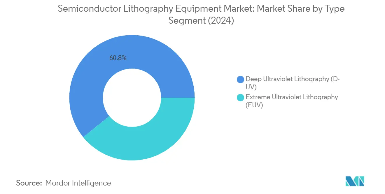
The Deep Ultraviolet Lithography (DUV) segment maintains its dominant position in the semiconductor lithography equipment market, holding approximately 61% market share in 2024. DUV lithography represents a critical optical projection lithography technique where patterns on masks are projected onto wafer surfaces through sophisticated 4X or 5X optical systems, primarily utilizing wavelengths of 248 nm or 193 nm. This technology has established itself as the backbone of IC manufacturing equipment, particularly excelling in large-area masters of discrete components within the typical 22 mm x 22 mm wafer-level exposure field size. The segment's strength lies in its cost-effectiveness, increased resolving power, and proven track record in supporting the semiconductor industry's miniaturization trends. Major semiconductor manufacturers continue to rely on DUV technology for printing complex patterns that characterize integrated circuits, particularly in producing lightweight electronic chips with lower power demands.
Extreme Ultraviolet Lithography Segment in Semiconductor Lithography Equipment Market
The Extreme Ultraviolet Lithography (EUV) segment is positioned as the fastest-growing segment in the semiconductor lithography equipment market, with an expected growth rate of approximately 12% from 2024 to 2029. This revolutionary technology utilizes light sources with extremely short wavelengths of 13.5 nanometers, enabling the production of increasingly sophisticated and miniaturized semiconductor components. The segment's rapid growth is driven by its crucial role in advancing chip manufacturing processes, particularly for server, network mobile, and supercomputing applications. EUV lithography equipment's ability to define finer and denser patterns than previous methods makes it indispensable for producing high-end processors on sub-10 nm nodes. The technology's capability to reduce the number of processing steps while achieving superior precision in circuit patterns continues to attract significant investments from leading semiconductor manufacturers worldwide.
Segment Analysis: By Application
MEMS Devices Segment in Semiconductor Lithography Equipment Market
The MEMS (Micro Electromechanical Systems) devices segment dominates the semiconductor lithography equipment market, holding approximately 55% of the market share in 2024. This significant market position is driven by the widespread deployment of MEMS devices in the automotive industry, including critical components like accelerometers, gyroscopes, and pressure sensors. The segment's dominance is further strengthened by the increasing adoption of MEMS technology in various applications such as autonomous vehicles, 5G infrastructure, smartphones, robotics, RF devices, and Advanced Driver Assistance Systems (ADAS). The lithography requirements for MEMS differ significantly from mainstream semiconductor industries, requiring higher depth of focus and accurate layer-to-layer alignment for optimal device performance, particularly in applications like gyroscopes and micro-mirrors.
Advanced Packaging Segment in Semiconductor Lithography Equipment Market
The advanced packaging segment is projected to exhibit the highest growth rate of approximately 9% during the forecast period 2024-2029. This accelerated growth is primarily attributed to the increasing focus on advanced packaging technologies as semiconductor geometries continue to shrink. The segment's growth is driven by the rising demand for various applications, including fan-out wafer level packaging (FO-WLP), fan-in wafer level chip scale packaging (WLCSP), flip-chip, and 2.5D/3D packaging solutions. These advanced packages require specialized lithography systems designed for creating redistribution layers (RDLs), silicon interposers, through silicon vias (TSVs), copper pillars, and micro-bumps on non-flat and reconstituted wafers, contributing to the segment's rapid expansion in the market.
Remaining Segments in Application Segmentation
The LED devices segment plays a crucial role in the semiconductor lithography equipment market, though smaller in market share compared to MEMS and advanced packaging segments. This segment is particularly significant in the manufacturing of high-brightness LEDs and other optoelectronic devices. The adoption of LED technology continues to grow across various applications, from automotive lighting to display technologies, driving the demand for specialized lithography equipment. The segment benefits from the increasing focus on energy-efficient lighting solutions and the growing adoption of LED technology in various consumer electronics applications, maintaining its important position in the overall market landscape.
Semiconductor Lithography Equipment Market Geography Segment Analysis
Semiconductor Lithography Equipment Market in North America
The North American semiconductor lithography equipment market maintains a significant position in the global landscape, holding approximately 10% of the market share in 2024. The region's dominance is primarily driven by its robust semiconductor manufacturing equipment R&D capabilities and substantial investments in expanding manufacturing capabilities. The United States, in particular, leads in semiconductor packaging innovation with numerous wafer fabrication plants spread across multiple states. The market is further strengthened by the rapid adoption of advanced technologies, including artificial intelligence, quantum computing, and sophisticated wireless networks like 5G. The presence of major technology hubs and research facilities continues to attract investments in semiconductor process equipment manufacturing infrastructure. Additionally, the growing demand for electric vehicles, consumer electronics, and IoT devices in the region has created a sustained need for advanced semiconductor manufacturing capabilities. The region's focus on technological sovereignty and reducing dependency on foreign semiconductor sources has led to increased investments in domestic manufacturing capabilities.
Semiconductor Lithography Equipment Market in Europe
The European semiconductor lithography equipment market has demonstrated robust growth, with an estimated growth rate of approximately 7% during the period 2019-2024. The region serves as home to some of the most crucial tech hubs globally and continues to be a significant driver and adopter of modern semiconductor technology. The market's growth is primarily fueled by the increasing demand for electric vehicles, clean energy solutions, expanding data centers, and automated manufacturing processes. European countries have been actively working to strengthen their position in the global semiconductor value chain through strategic investments and partnerships. The presence of major lithography equipment manufacturers, particularly in countries like the Netherlands, has established Europe as a crucial player in the global market. The region's strong focus on research and development, coupled with its advanced technological infrastructure, continues to drive innovation in semiconductor manufacturing processes. The market is further supported by the growing adoption of IoT devices, artificial intelligence, and other emerging technologies across various industries.
Semiconductor Lithography Equipment Market in Asia-Pacific
The Asia-Pacific semiconductor lithography equipment market is projected to experience substantial growth at a rate of approximately 8% during the period 2024-2029. The region has established itself as the global hub for semiconductor manufacturing, with countries like China, Taiwan, South Korea, and Japan leading the way. The market's robust growth is driven by the presence of large chip manufacturing equipment, packaging, and assembly industries. The region benefits from supportive government regulations, readily available raw materials, and a skilled labor force. The increasing penetration of digital technologies, rapid urbanization, and industrialization continue to fuel market expansion. Major semiconductor manufacturers in the region are actively investing in advanced manufacturing capabilities and expanding their production facilities. The market is characterized by intense competition and continuous technological advancement, particularly in areas such as extreme ultraviolet (EUV) lithography and advanced packaging solutions. The region's strong focus on developing domestic semiconductor capabilities has led to significant investments in research and development.
Semiconductor Lithography Equipment Market in Rest of the World
The Rest of the World market for semiconductor lithography equipment, encompassing regions across Latin America, the Middle East, and Africa, represents an emerging opportunity in the global landscape. These regions are experiencing increasing demand for semiconductor manufacturing capabilities driven by growing urbanization, infrastructural development, and the rising penetration of digital technologies. The market is primarily dominated by international players who are gradually expanding their presence in these regions. Countries in the Middle East, particularly in the GCC region, are showing increased interest in developing domestic semiconductor capabilities as part of their economic diversification strategies. Latin American countries are focusing on strengthening their semiconductor manufacturing capabilities to reduce dependency on imports. The market is characterized by growing investments in technological infrastructure and increasing adoption of advanced manufacturing processes. Government initiatives to attract semiconductor manufacturers and develop local expertise are creating new opportunities for market growth. The region's potential for market expansion is further supported by the increasing demand for consumer electronics, automotive applications, and industrial automation.
Semiconductor Lithography Equipment Industry Overview
Top Companies in Semiconductor Lithography Equipment Market
The semiconductor lithography equipment market is dominated by established players like ASML Holding NV, Canon Inc., Nikon Corporation, and JEOL Ltd, who have maintained their market positions through continuous innovation and strategic investments. These companies focus on developing advanced lithography solutions, particularly in EUV and DUV technologies, to meet the increasing demands of semiconductor manufacturers. The industry witnesses significant investments in research and development, with companies expanding their manufacturing facilities and forming strategic partnerships to enhance their technological capabilities. Market leaders are actively pursuing innovations in areas such as maskless exposure technology, advanced packaging solutions, and high-resolution imaging systems. Companies are also establishing regional centers for training, demonstration, and solution development to strengthen their presence in key markets like South Korea, Taiwan, and China.
Consolidated Market with High Entry Barriers
The semiconductor manufacturing equipment market exhibits a highly consolidated structure dominated by global conglomerates with extensive technological expertise and manufacturing capabilities. These established players have built strong barriers to entry through their intellectual property portfolios, long-standing customer relationships, and significant capital investments in research and development. The market's complexity is further heightened by the need for specialized knowledge in areas such as optical systems, precision engineering, and semiconductor manufacturing processes. The high cost of developing and manufacturing lithography equipment, coupled with the extensive certification and qualification requirements, makes it challenging for new entrants to gain a foothold in the market.
The industry has witnessed strategic mergers and acquisitions aimed at expanding technological capabilities and market reach. Companies are increasingly focusing on vertical integration to strengthen their control over critical components and technologies. The market structure is characterized by long-term relationships between equipment manufacturers and semiconductor fabrication facilities, creating a stable but competitive environment. Regional players, particularly in Asia, are emerging with government support and subsidies, though they primarily focus on specific market segments or regional opportunities rather than competing directly with global leaders in cutting-edge technology segments.
Innovation and Adaptability Drive Market Success
Success in the semiconductor lithography equipment market increasingly depends on companies' ability to innovate and adapt to rapidly evolving technological requirements. Market leaders must maintain substantial investments in research and development to stay ahead of the technology curve, particularly in areas like EUV lithography and advanced packaging solutions. Companies need to develop comprehensive service networks and maintain close relationships with semiconductor manufacturers to understand and address their evolving needs. The ability to provide integrated solutions that combine hardware excellence with advanced software capabilities has become crucial for maintaining market position.
For contenders looking to gain market share, focusing on specific market segments or regional opportunities presents a viable strategy. Success factors include developing cost-effective solutions for mature technology nodes, establishing a strong local presence in growing markets, and building partnerships with established players. The industry's regulatory environment, particularly regarding export controls and technology transfer, significantly impacts market dynamics and requires careful navigation. Companies must also consider the concentration of end-users in specific regions and develop strategies to serve these markets effectively while managing supply chain risks and maintaining technological competitiveness. Additionally, the integration of wafer processing equipment into comprehensive solutions is becoming increasingly important.
Semiconductor Lithography Equipment Market Leaders
-
Canon Inc.
-
Nikon Corporation
-
ASML Holding NV
-
Veeco Instruments Inc.
-
SÜSS MicroTec SE
- *Disclaimer: Major Players sorted in no particular order
Semiconductor Lithography Equipment Market News
- December 2022 - Canon Inc. launched an i-line lithography stepper for 3D advanced packaging, such as those used with chiplets mounted on an interposer. The FPA-5520iV LF2, based on 365nm wavelength light, is optimized for back-end processing and delivers 0.8-micron resolution across a 52 mm by 68 mm single-exposure field. A four-shot mode extends the area to 100 mm by 100 mm.
- November 2022 - EVG (EV Group), a provider of lithography equipment and wafer bonding for the MEMS, nanotechnology, and semiconductor markets, strengthened its optical lithography solutions portfolio with the launch of the next-generation 200-mm version of its EVG 150 automated resist processing system.
Semiconductor Lithography Equipment Industry Segmentation
A semiconductor lithography system at its core is a projection system. This equipment is used to draw highly complex circuit patterns on a photomask that is usually made of large glass plates. To do this, these types of equipment reduce the size of the circuit pattern using ultra-high-performance lenses and expose them onto a silicon substrate called a wafer. The lithography equipment is broadly categorized into dry and immersion types, and the EUV lithography machine is considered the most advanced.
The market for semiconductor lithography equipment was evaluated by analyzing separate market sizes for deep ultraviolet lithography (DUV) (ArFi, ArF dry, KrF, i-line) and extreme ultraviolet lithography (EUV) for different applications, including advanced packaging, MEMS devices, and LED devices in multiple geographies, including North America, Europe, Asia-Pacific, and the Rest of the World. The study also examines the impact of macroeconomic trends on the market and impacted segments. The study also discusses the drivers and restraints likely to influence the market's evolution in the near future. The market sizes and forecasts are provided in terms of USD value for all the above segments.
| Type | Deep Ultraviolet Lithography (DUV) |
| Extreme Ultraviolet Lithography (EUV) | |
| Application | Advanced Packaging |
| MEMS Devices | |
| LED Devices | |
| Geography | North America |
| Europe | |
| Asia | |
| Australia and New Zealand | |
| Latin America | |
| Middle East and Africa |
| Deep Ultraviolet Lithography (DUV) |
| Extreme Ultraviolet Lithography (EUV) |
| Advanced Packaging |
| MEMS Devices |
| LED Devices |
| North America |
| Europe |
| Asia |
| Australia and New Zealand |
| Latin America |
| Middle East and Africa |
Semiconductor Lithography Equipment Market Research FAQs
How big is the Semiconductor Lithography Equipment Market?
The Semiconductor Lithography Equipment Market size is expected to reach USD 28.43 billion in 2025 and grow at a CAGR of 7.38% to reach USD 40.59 billion by 2030.
What is the current Semiconductor Lithography Equipment Market size?
In 2025, the Semiconductor Lithography Equipment Market size is expected to reach USD 28.43 billion.
Who are the key players in Semiconductor Lithography Equipment Market?
Canon Inc., Nikon Corporation, ASML Holding NV, Veeco Instruments Inc. and SÜSS MicroTec SE are the major companies operating in the Semiconductor Lithography Equipment Market.
Which is the fastest growing region in Semiconductor Lithography Equipment Market?
Asia Pacific is estimated to grow at the highest CAGR over the forecast period (2025-2030).
Which region has the biggest share in Semiconductor Lithography Equipment Market?
In 2025, the Asia Pacific accounts for the largest market share in Semiconductor Lithography Equipment Market.
What years does this Semiconductor Lithography Equipment Market cover, and what was the market size in 2024?
In 2024, the Semiconductor Lithography Equipment Market size was estimated at USD 26.33 billion. The report covers the Semiconductor Lithography Equipment Market historical market size for years: 2019, 2020, 2021, 2022, 2023 and 2024. The report also forecasts the Semiconductor Lithography Equipment Market size for years: 2025, 2026, 2027, 2028, 2029 and 2030.

