Semiconductor Lead Frame Market Size and Share
Market Overview
| Study Period | 2020 - 2031 |
|---|---|
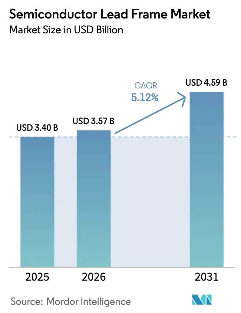
| Market Size (2026) | USD 3.57 Billion |
| Market Size (2031) | USD 4.59 Billion |
| Growth Rate (2026 - 2031) | 5.12% CAGR |
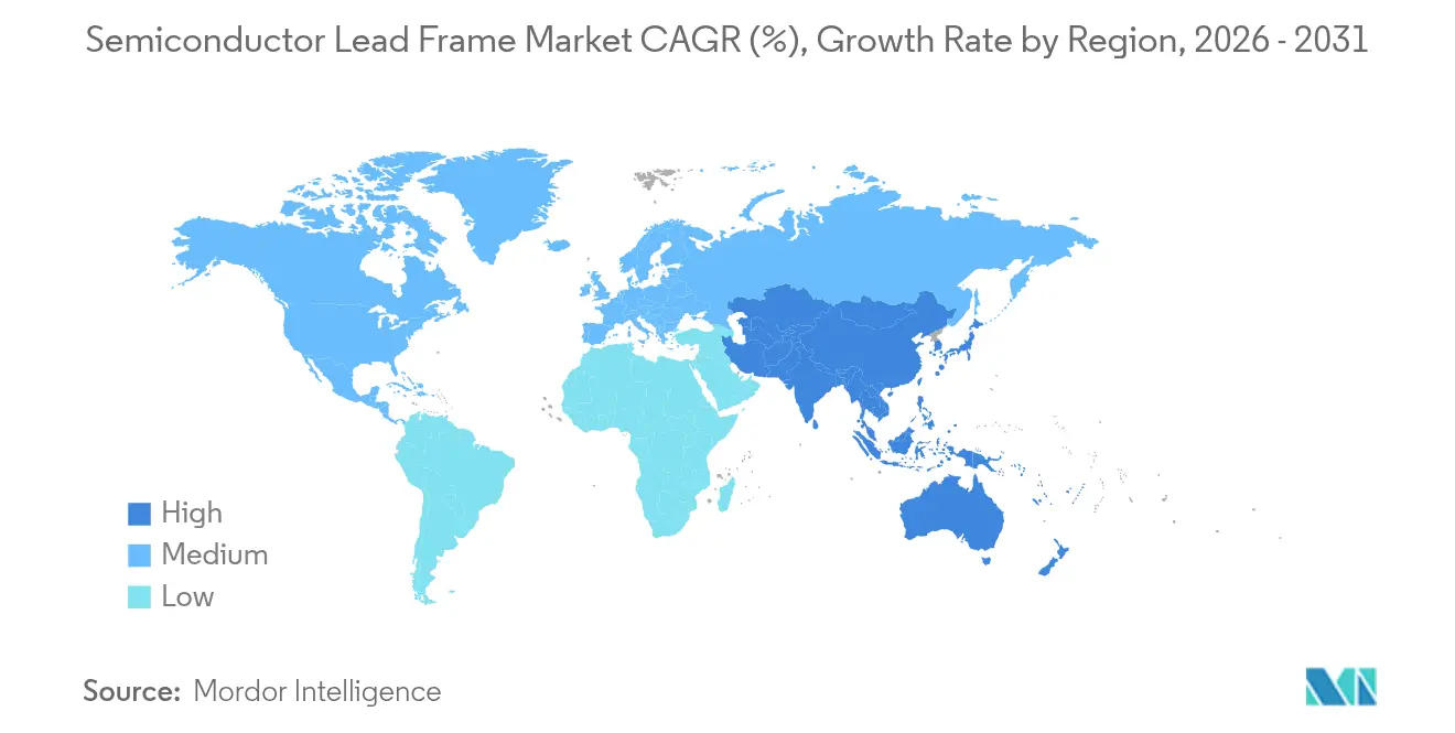
| Fastest Growing Market | Asia Pacific |
| Largest Market | Asia Pacific |
| Market Concentration | Medium |
Major Players *Disclaimer: Major Players sorted in no particular order Image © Mordor Intelligence. Reuse requires attribution under CC BY 4.0. | |
Semiconductor Lead Frame Market Analysis by Mordor Intelligence
The semiconductor lead frame market size was valued at USD 3.40 billion in 2025 and estimated to grow from USD 3.57 billion in 2026 to reach USD 4.59 billion by 2031, at a CAGR of 5.12% during the forecast period (2026-2031). Demand accelerated as automotive electronics, 5G infrastructure, and AI-enabled edge devices required compact packages that dissipate heat effectively while supporting high-speed signals. Miniaturization shifted unit volumes toward Quad Flat No-Lead (QFN) and Dual Flat No-Lead (DFN) variants, and power-electronics adoption in electric vehicles (EVs) lifted specifications for copper-based frames able to endure higher thermal loads. Regionalization of supply chains gathered momentum as the CHIPS Act prompted fresh capacity in North America and Europe, complementing entrenched production hubs in Asia-Pacific. At the same time, composite and multi-layer structures gained traction as material innovations aimed to counter copper and silver price volatility and support silicon carbide (SiC) and gallium nitride (GaN) technologies.
Key Report Takeaways
- By packaging type, QFN led with 31.65% of the semiconductor lead frame market share in 2025; DFN is projected to expand at an 8.45% CAGR through 2031.
- By manufacturing process, stamping dominated with 62.75% revenue share in 2025, whereas multi-layer/composite frames are forecast to grow at a 9.05% CAGR to 2031.
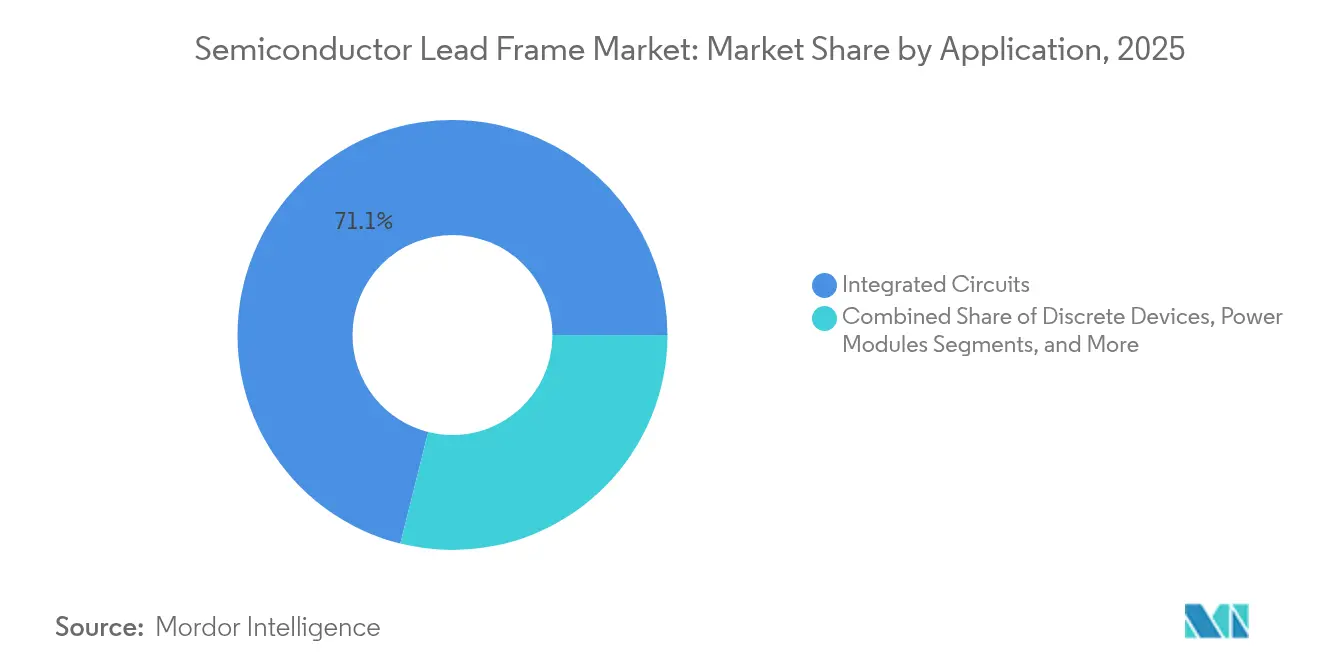
- By application, integrated circuits accounted for a 71.10% share of the semiconductor lead frame market size in 2025, while power modules are advancing at a 9.35% CAGR through 2031.
- By industry vertical, consumer electronics held 45.05% of the semiconductor lead frame market share in 2025; automotive is projected to grow fastest at an 11.1% CAGR between 2026-2031.
- By geography, Asia-Pacific commanded 41.10% revenue share in 2025 and is expected to post the highest 8.75% CAGR to 2031.
Note: Market size and forecast figures in this report are generated using Mordor Intelligence’s proprietary estimation framework, updated with the latest available data and insights as of 2026.
Global Semiconductor Lead Frame Market Trends and Insights
Drivers Impact Analysis*
| Driver | (~) % Impact on CAGR Forecast | Geographic Relevance | Impact Timeline |
|---|---|---|---|
| Consumer-electronics demand spike | +1.2% | Global, with a concentration in Asia-Pacific | Short term (≤ 2 years) |
| EV and xEV power-electronics boom | +1.8% | North America, Europe, China | Medium term (2-4 years) |
| 5G/AI edge devices needing QFN/QFP | +1.3% | Global, with early adoption in North America and East Asia | Medium term (2-4 years) |
| Asia-Pacific capacity additions | +0.9% | Asia-Pacific, with spillover benefits to the global supply chain | Short term (≤ 2 years) |
| SiC/GaN modules favour Cu lead frames | +1.1% | North America, Europe, Japan | Long term (≥ 4 years) |
| CHIPS-Act-driven on-shore packaging CAPEX | +0.7% | North America, Europe | Medium term (2-4 years) |
| Source: Mordor Intelligence | |||
Consumer-electronics demand spike
Surging smartphone, wearable, and gaming-device shipments in 2024 and early 2025 tightened product-development cycles and pushed designers toward slimmer QFN outlines that improved thermal paths without enlarging footprints. Roughly one quarter of global output already uses lead-frame thicknesses below 0.1 mm, enabling higher component density inside premium mobiles.[1]ASE Kaohsiung, “Lead Frame,” asekh.aseglobal.com Several OSAT providers extended automotive-qualified flows to consumer lines, promoting Grade-0 reliability in handheld products that faced frequent temperature swings. These shifts sustained the semiconductor lead frame market as device makers balanced battery life, weight, and performance requirements.
EV and xEV power-electronics boom
Electric-vehicle production climbed sharply, and traction inverters shifted from 400 V to 800 V architectures. Lead frames, therefore, require copper alloys with improved thermal conductivity and fatigue strength. ROHM’s TRCDRIVE pack™ SiC module illustrated the need for optimized heat spreading to maintain low switching losses up to 300 kW. Tier-1 suppliers specified composite frames that paired stamped copper with plated nickel-palladium finishes to control corrosion over extended vehicle lifetimes. The automotive procurement wave broadened revenue visibility and anchored long-term orders within the semiconductor lead frame market.
5G/AI edge devices needing QFN/QFP
Fifth-generation radio units and on-device AI accelerators demanded multi-chip packages that guard signal integrity above 10 GHz. Semiconductor foundries adopted 2.5D bridges such as Embedded Multi-Chip Interconnect Bridge (EMIB) and vertical Foveros stacks, both of which rely on precision-etched lead frames to minimize impedance mismatch. Material suppliers introduced oxygen-free high-conductivity (OFHC) copper grades and refined surface finishes to suppress parasitic. These requirements lifted average selling prices and underpinned premium tiers within the semiconductor lead frame industry.
Asia-Pacific capacity additions
Capital deployments in China, Japan, India, Vietnam, and Malaysia shortened regional lead times and introduced specialized lines for automotive and 5G products. Micron announced a USD 825 million assembly facility in Gujarat targeted at advanced test flows, creating a skilled-labour cluster projecting 20,000 total jobs. Parallel training programs, such as Lam Research’s Semiverse Solution, widened local engineering talent pools. These developments reinforced Asia-Pacific’s central role but also diversified production nodes, reducing single-country exposure inside the semiconductor lead frame market.
Restraints Impact Analysis*
| Restraint | (~) % Impact on CAGR Forecast | Geographic Relevance | Impact Timeline |
|---|---|---|---|
| CAPEX intensity and production bottlenecks | -1.1% | Global, with higher impact in emerging markets | Medium term (2-4 years) |
| Copper and Ag price volatility | -0.8% | Global, with a pronounced effect on high-volume manufacturers | Short term (≤ 2 years) |
| Shift to glass/organic interposers | -0.6% | North America, East Asia | Long term (≥ 4 years) |
| Stricter plating-chemical regulations | -0.5% | Europe, North America, with gradual adoption in Asia | Medium term (2-4 years) |
| Source: Mordor Intelligence | |||
CAPEX intensity and production bottlenecks
Turnkey stamping lines with fine-pitch capability exceeded USD 300 million per site, and tooling costs rose as die pads shrank. Smaller vendors faced liquidity strains, pushing some to merge or license capacity from larger OSATs. High automation levels, including AI-enabled defect-inspection networks with 95% accuracy, partially offset labour shortages but lengthened ramp timelines. Capacity tightness occasionally delays customer qualifications, creating a headwind for the semiconductor lead frame market.
Copper and Ag price volatility
Average copper prices climbed beyond 380 cents per pound in early 2024 and swung widely throughout the year. Lead frame suppliers rectified margin pressures by hedging, introducing scrap-based closed-loop recycling, and shifting to layered composites that diluted pure copper content without hurting electrical performance. Adherence to the Copper Mark Assurance Framework improved traceability but increased compliance overhead, marginally dampening profitability across parts of the semiconductor lead frame industry.
*Our forecasts treat driver/restraint impacts as directional, not additive. The impact forecasts reflect baseline growth, mix effects, and variable interactions.
Segment Analysis
By Packaging Type: QFN dominance persists while DFN accelerates
QFN packages captured 31.65% of 2025 volumes, confirming their role as the preferred choice for thermal efficiency in limited board area. The segment’s evolution toward smaller lead pitches and center pads bolstered reliability in automotive sensors and premium smartphones. DFN units, projected to deliver an 8.45% CAGR to 2031, offered even thinner profiles suited to wearables and compact IoT end-nodes. Together, QFN and DFN sustained healthy revenue streams that kept the semiconductor lead frame market on its upward trajectory.
Advances such as drop-in heat slugs and double-die stacking expanded QFP use cases, while DIP and SOP packages gradually migrated to legacy or industrial markets where cost outweighed miniaturization. Flip-chip outlines served high-performance computing but required plated copper pillars rather than exposed leads. Across the category, the semiconductor lead frame market size for QFN and DFN was forecast to outpace wider industry growth, driven by continuous smartphone refresh cycles and regulatory pushes for lighter in-car modules.


By Manufacturing Process: stamping efficiency underpins the share
Stamping maintained 62.75% of 2025 production thanks to high-speed presses exceeding 90,000 strokes per hour and modular die sets that reduced changeover time. Continuous strip plating added selective finishes that limited precious-metal usage. Multi-layer composites, however, are expected to register a 9.05% CAGR through 2031 as designers combine copper cores with inlaid molybdenum or aluminium for thermal spreading. These premium configurations reflect the semiconductor lead frame market’s response to EV inverter stress conditions.
Etching found a share in small-lot, high-precision circuits for 5G beamformers and optical modules. Laser-assisted photoresist exposure improved edge acuity, allowing ±5 µm dimensional control. As complexity rose, the semiconductor lead frame industry allocated research and development toward hybrid flows that used etching for fine features and stamping for mechanical robustness, balancing cost and performance under tightened product-launch windows.
By Application: integrated circuits dominate, power modules surge
Integrated circuits accounted for 71.10% of packages shipped in 2025, spanning microcontrollers, analog front ends, and connectivity chips. High volume and standardization anchored stable capacity utilization, reinforcing economies of scale within the semiconductor lead frame market. Power modules, forecast to grow at 9.35% CAGR, benefited from SiC devices’ migration into drivetrain inverters and renewable-energy converters, demanding lead frames with low thermal resistance and high creepage distance.
MEMS and sensor assemblies proliferated in smart factories and medical wearables, leveraging nickel-palladium-gold plating to safeguard bond wires against corrosion. The semiconductor lead frame market size for sensor applications is set to climb as industrial automation deploys condition-monitoring nodes across machinery fleets. Discrete devices, though mature, remained essential in voltage-regulation stages, affirming a diversified mix that stabilizes overall industry revenue.
By Industry Vertical: consumer electronics leads, automotive accelerates
Consumer electronics preserved a 45.05% revenue share in 2025, powered by handset updates, augmented-reality headsets, and home-entertainment upgrades. Suppliers delivered ultrathin DFN outlines that freed board area for larger batteries. Automotive electronics, expanding at 11.1% CAGR, demanded mission-profile testing and AEC-Q100 certification, nudging OSATs to segregate automotive lines for zero-defect goals and traceability. These shifts elevated ASPs and buoyed margins across the semiconductor lead frame market.
Industrial automation and telecom infrastructure posted steady mid-single-digit expansion. 5G macro radios and open-RAN units embraced QFPs with integrated heat slugs, enabling efficient base-station cooling in dense city deployments. Aerospace and defense, and medical sectors remained niche but margin-rich, requiring hermetic sealing and long lifecycle support that few specialists offer, illustrating the segmentation depth inside the semiconductor lead frame industry.
Geography Analysis
Asia-Pacific held 41.10% of global revenue in 2025 and was expected to log a 8.75% CAGR through 2031. China shipped more than 42 billion stamped frames, while Japan’s precision-etch specialists supplied high-frequency modules for driver-assistance systems. Investments exceeding USD 300 million in Vietnam and Malaysia upgraded plating lines to support SiC power hybrids.
North America saw renewed impetus from the CHIPS Act, which earmarked USD 39 billion for fabrication expansion and USD 13.2 billion for R&D. Fab capacity was projected to rise 203% by 2032, creating demand for domestically sourced frames that matched heterogeneous-integration roadmaps. Intel’s EMIB and Foveros programs required custom copper-alloy compositions, adding value layers that differentiated suppliers.
Europe concentrated on high-reliability automotive and industrial uses, supported by the Euro 43 billion (USD 49.90 billion) European Chips Act, aiming for 20% global semiconductor output by 2030. Limited local IC-substrate capability left white-space for new entrants ready to establish composite or etched-frame lines near Germany’s car manufacturers. Raw-material price escalation—copper up 9% and aluminium up 8%—drove European firms to explore recycling initiatives that aligned with carbon-reduction mandates, reinforcing supply-chain resilience in the semiconductor lead frame industry.

Competitive Landscape
The top ten suppliers controlled the majority of the global shipments share in 2024, indicating a moderately concentrated field. Leading players expanded facilities, integrated AI-driven vision systems, and refined selective-plating chemistries to shrink cycle times.[4]Tingrui Sun et al., “Cascaded Detection Method for Surface Defects of Lead Frame,” Journal of Manufacturing Systems, doi.org Smaller specialists pivoted toward composite frames for SiC modules or ultra-fine DFN outlines, commanding premium unit prices. Patent-backed designs, such as plated end leads with recesses that improved solder-joint integrity, further differentiated offerings.
Digital-twin platforms simulated punch-die stress and thermal fatigue, enabling predictive maintenance that lifted average press uptime beyond 92%. Medium-sized firms licensed such analytics to broaden their service portfolios. Vertical integration across alloy rolling, stamping, and plating improved cost control during volatile commodity cycles. Partnerships between automotive Tier-1 suppliers and semiconductor firms accelerated the co-development of platform-specific solutions, solidifying strategic moats inside the semiconductor lead frame market.
Capacity expansions were announced in India, Japan, and Arizona, reflecting a shift toward multi-regional footprints. Suppliers diversified customer bases to hedge geopolitical risk, while material-recycling initiatives gained prominence to meet ESG targets. Overall, evolving technology nodes, regional incentives, and sustainability imperatives collectively reshaped competitive tactics across the semiconductor lead frame industry.
Semiconductor Lead Frame Industry Leaders
Mitsui High-tec, Inc.
SHINKO ELECTRIC INDUSTRIES CO., LTD.
ASM Pacific Technology Ltd.
Chang Wah Technology Co., Ltd.
Amkor Technology Inc.
- *Disclaimer: Major Players sorted in no particular order

Recent Industry Developments
- April 2025: ASE Technology Holding Co., Ltd. reported 50.9% of 2024 packaging revenue stemmed from communications, computing, and consumer electronics, highlighting raw-material supply-chain risks.
- April 2025: Mitsubishi Materials Corporation and Masan High-Tech Materials Group finalized the purchase of HC Starck Tungsten to enhance global alloy reach.
- March 2025: Intel portrayed its global foundry strategy, adding advanced-packaging capacity across Arizona, New Mexico, Ireland, and Malaysia to achieve the number-two foundry position by 2030.
- March 2025: JX Advanced Metals Corporation disclosed a three-year, 270 billion yen (USD 1.85 billion), plan to enlarge sputtering-target output in Ibaraki and Mesa, serving AI and EV demand.


Research Methodology Framework and Report Scope
Market Definitions and Key Coverage
Our study defines the semiconductor lead frame market as revenues generated from newly manufactured metallic frames that secure and electrically connect packaged integrated circuits, discrete devices, and power modules. These frames are usually stamped or chemically etched from copper-based alloys and shipped to assembly houses that mold, wire-bond, and test finished packages.
Scope exclusion: Printed circuit board interposers and organic laminate substrates are outside this lead-frame scope.
Segmentation Overview
- By Packaging Type
- DIP (Dual In-Line Package)
- SOP (Small Outline Package)
- SOT (Small Outline Transistor)
- QFP (Quad Flat Pack)
- DFN (Dual Flat No-Lead)
- QFN (Quad Flat No-Lead)
- FC and TO Packages
- By Manufacturing Process
- Stamping Lead Frame
- Etching Lead Frame
- Multi-layer / Composite
- By Application
- Integrated Circuits
- Discrete Devices
- Power Modules
- MEMS and Sensors
- By Industry Vertical
- Consumer Electronics
- Automotive
- Industrial and Commercial Electronics
- Telecommunications
- Aerospace and Defence
- Medical Devices
- By Geography
- North America
- United States
- Canada
- South America
- Brazil
- Argentina
- Rest of South America
- Europe
- Germany
- United Kingdom
- France
- Italy
- Russia
- Rest of Europe
- Asia-Pacific
- China
- Japan
- South Korea
- India
- ASEAN
- Rest of Asia-Pacific
- Middle East and Africa
- Middle East
- GCC
- Rest of Middle East
- Africa
- South Africa
- Rest of Africa
- Middle East
- North America
Detailed Research Methodology and Data Validation
Primary Research
Mordor analysts interviewed packaging engineers, alloy strip suppliers, and procurement managers in Asia, North America, and Europe to verify lead-frame unit yields, gauge average selling prices, and test preliminary forecasts before locking our model.
Desk Research
We began with public domain series from authorities such as JEITA, SEMI, UN Comtrade customs codes 854890, WSTS semiconductor billings, and the OECD copper price index, which give foundational signals on device output, trade flows, and material cost trends. Annual reports and 10-Ks of major outsourced assembly and test players, along with patent filings pulled from Questel, helped our team size proprietary capacity and technology adoption. Subscription feeds from D&B Hoovers and Dow Jones Factiva supplied shipment guidance and contract wins that refine regional splits. These sources illustrate the market but are not exhaustive; many others supported data checks, validation, and clarifications.
Market-Sizing & Forecasting
A top-down device production reconstruction was employed, starting with worldwide IC and discrete output, which is then filtered through package-mix shares to isolate the demand pool for stamped and etched frames. Selective bottom-up roll-ups of major suppliers' shipments served as guardrails. Key model variables include global smartphone shipments, 5G base-station counts, electric vehicle output, copper alloy price movements, and average lead-frame ASP progression. Multivariate regression links these drivers to frame demand, while scenario analysis stress tests currency shifts and capacity additions. Where supplier disclosures were thin, gap values were benchmarked against historical utilization norms and channel checks.
Data Validation & Update Cycle
Model outputs pass three layers of anomaly checks, peer reviews, and senior analyst approval. We refresh every twelve months and trigger interim updates if raw material costs spike, major capacity comes online, or new regulatory directives reshape package selection.
Why Mordor's Semiconductor Lead Frame Baseline Commands Unmatched Reliability
Published estimates often diverge; different firms choose unlike package scopes, currency years, and refresh cadences, so headline numbers rarely align.
Key gap drivers appear when others fold laminate substrates into totals, apply uniform ASP growth, or freeze assumptions for several years, whereas Mordor revisits copper inputs quarterly and rebalances package-mix shares after each major assembly plant expansion.
Benchmark comparison
| Market Size | Anonymized source | Primary gap driver |
|---|---|---|
| USD 3.40 B (2025) | Mordor Intelligence | - |
| USD 4.08 B (2024) | Regional Consultancy A | Includes laminate substrates and organic interposers |
| USD 3.48 B (2023) | Global Consultancy B | Older base year, inflation not normalized to 2025 dollars |
| USD 3.59 B (2024) | Industry Journal C | Limited package mix detail, static ASP escalation |
The comparison shows how our disciplined scope, live cost tracking, and annual refresh give decision-makers a balanced, transparent baseline that is traceable to clear variables and repeatable steps.


Key Questions Answered in the Report
What is the expected growth rate of the semiconductor lead frame market between 2026 and 2031?
The market is projected to expand at a 5.12% CAGR, rising from USD 3.57 billion in 2026 to USD 4.59 billion by 2031.
Which packaging type generates the highest revenue at present?
QFN packages led with a 31.65% share in 2025 due to their favourable thermal and size characteristics.
Why are automotive applications important for future demand?
Automotive electronics, especially EV power modules, are forecast to grow at an 11.1% CAGR, driving the need for high-thermal-performance copper alloy frames.
How is regional policy affecting supply chains?
The CHIPS Act in the United States and the European Chips Act in the EU are stimulating new local capacity, reducing reliance on Asia-Pacific production hubs.
What manufacturing process dominates the semiconductor lead frame industry today?
Stamping holds 62.75% of 2025 output thanks to its cost efficiency and suitability for large-volume runs, though composite frames are gaining share.
How are material price swings being managed by suppliers?
Companies are investing in recycling, composite structures, and hedging strategies to limit exposure to copper and silver price volatility.
Page last updated on:


