Semiconductor Industry Size and Share
Market Overview
| Study Period | 2020 - 2031 |
|---|---|
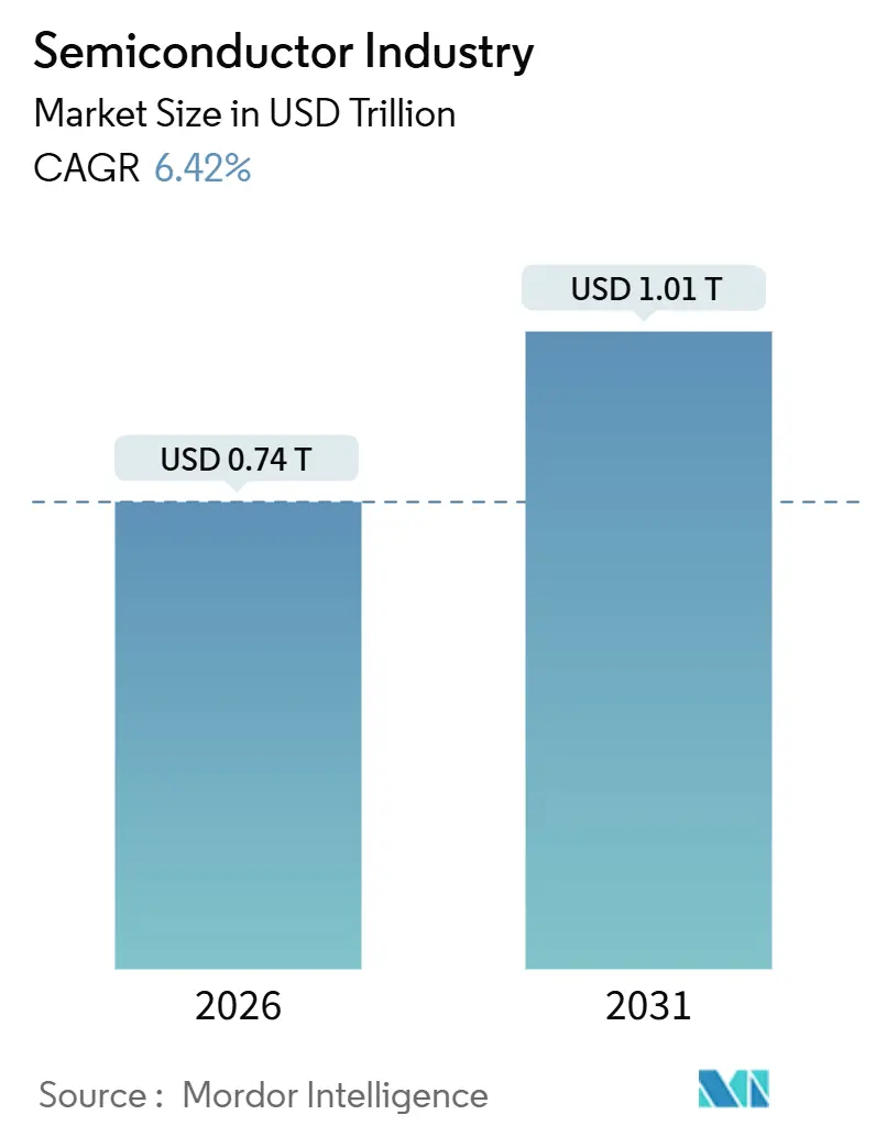
| Market Size (2026) | USD 0.74 Trillion |
| Market Size (2031) | USD 1.01 Trillion |
| Growth Rate (2026 - 2031) | 6.42% CAGR |
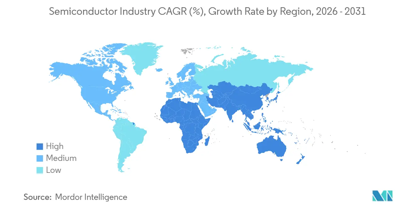
| Fastest Growing Market | Middle East |
| Largest Market | Asia Pacific |
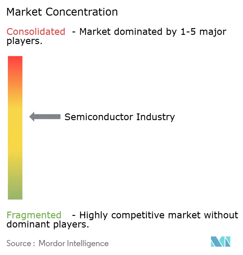
| Market Concentration | Medium |
Major Players *Disclaimer: Major Players sorted in no particular order Image © Mordor Intelligence. Reuse requires attribution under CC BY 4.0. | |
Semiconductor Industry Analysis by Mordor Intelligence
The semiconductor industry size stood at USD 0.74 trillion in 2026 and is projected to reach USD 1.01 trillion by 2031, implying a 6.42% CAGR and confirming steady structural expansion. Accelerated purchases of artificial intelligence accelerators by hyperscale data-center operators, rising silicon content per electric vehicle, and sovereign subsidies for on-shoring are expanding the revenue base even as unit sales of smartphones and personal computers plateau. Chiplet-ready heterogeneous packages are lowering capital barriers for fabless challengers, spawning a broader competitive field across logic, memory, and advanced packaging. Meanwhile, geopolitical export controls are reshaping wafer flows and pushing mature-node investment toward regions that can guarantee supply-chain sovereignty. Water availability, power reliability, and advanced-lithography tool supply now weigh as heavily on profitability as classic cost and yield metrics.
Key Report Takeaways
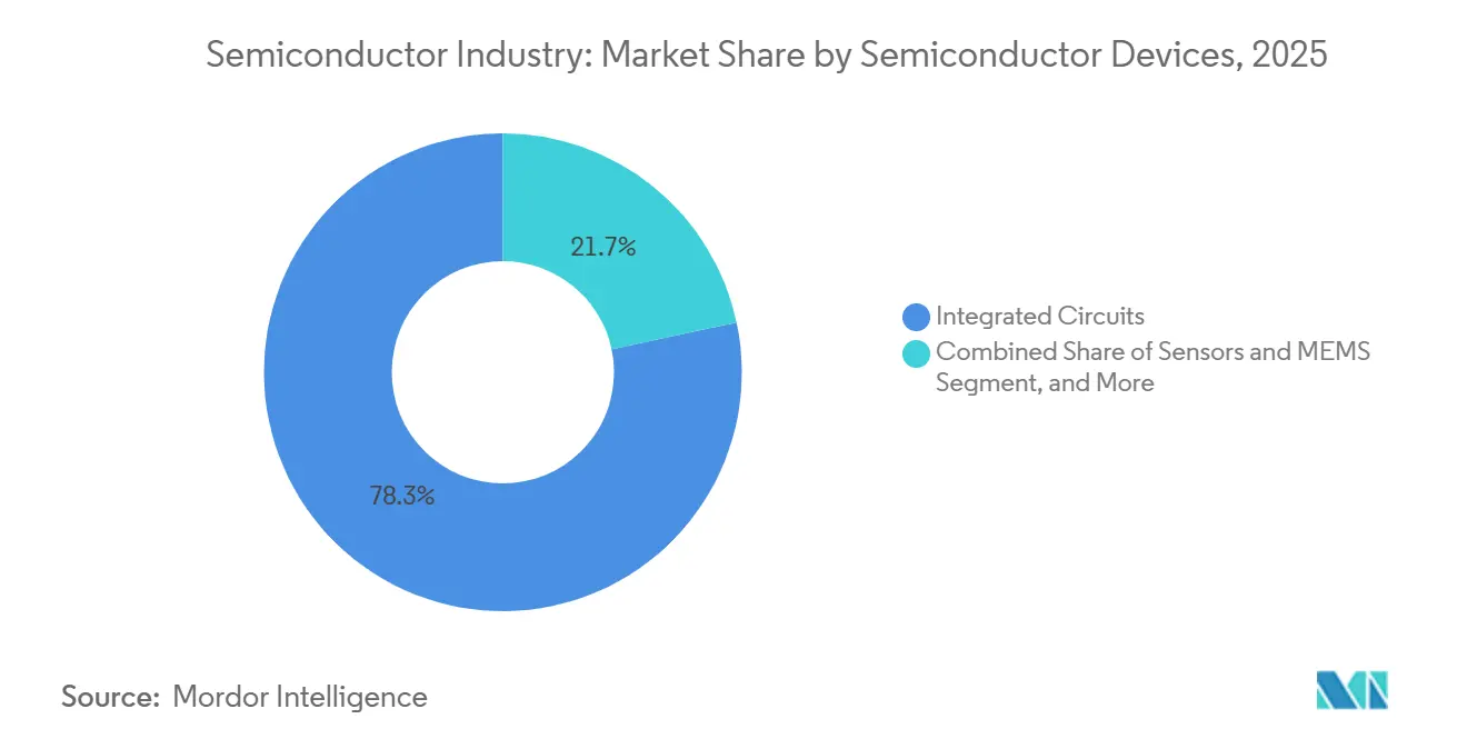
- By semiconductor devices, integrated circuits led with 78.33% of the semiconductor industry share in 2025, while sensors and MEMS are projected to post the fastest 8.49% CAGR through 2031.
- By business model, integrated device manufacturers commanded 54.78% of the semiconductor industry share in 2025, whereas design and fabless vendors are poised to expand at a 6.96% CAGR to 2031.
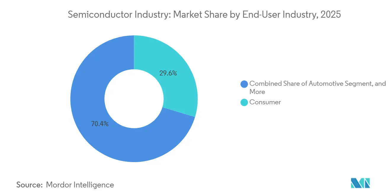
- By end-user industry, consumer electronics accounted for the largest 29.63% of the semiconductor industry share in 2025, while automotive semiconductors are forecast to grow at an 8.91% CAGR through 2031.
- By geography, Asia Pacific captured 59.69% of 2025 revenue, whereas the Middle East is expected to register the fastest CAGR of 8.51% over the forecast period.
Note: Market size and forecast figures in this report are generated using Mordor Intelligence’s proprietary estimation framework, updated with the latest available data and insights as of January 2026.
Global Semiconductor Industry Trends and Insights
Drivers Impact Analysis*
| Driver | (~) % Impact on CAGR Forecast | Geographic Relevance | Impact Timeline |
|---|---|---|---|
| Explosive Data-Center Demand for AI Accelerators | +1.8% | Global, concentrated in North America and Asia Pacific | Short term (≤ 2 years) |
| Ubiquitous Edge-AI in Consumer IoT Devices | +1.2% | Global, led by Asia Pacific manufacturing hubs | Medium term (2-4 years) |
| Automotive Zonal-Architecture Migration | +1.5% | Global, early adoption in Europe and North America | Medium term (2-4 years) |
| On-shoring Incentives in United States, European Union, India and Middle East and Africa | +0.9% | North America, Europe, Middle East and Africa and India | Long term (≥ 4 years) |
| Heterogeneous Integration Cost-Down Inflection | +0.7% | Global, advanced-packaging hubs in Asia Pacific | Medium term (2-4 years) |
| Chiplet Marketplace Commercialization | +0.6% | Global, fabless design centers in North America and Asia | Long term (≥ 4 years) |
| Source: Mordor Intelligence | |||
Explosive Data-Center Demand for AI Accelerators
Hyperscale operators deployed more than 1.5 million graphics processing units for generative AI training in 2025, fully absorbing Taiwan Semiconductor Manufacturing Company’s 4-nanometer and 5-nanometer capacity and stretching substrate lead-times beyond 40 weeks. NVIDIA’s data-center revenue hit USD 30.8 billion in the third quarter of fiscal 2025, accounting for 87% of sales, while Advanced Micro Devices captured roughly 15% of the accelerator segment with initial MI300 shipments.[1]NVIDIA Corporation, “Quarterly Results,” NVIDIA Investor Relations, nvidia.com The pivot from training to inference is boosting demand for low-precision arithmetic cores that deliver higher throughput per watt, a profile well suited to application-specific integrated circuits. High-bandwidth memory shipments climbed 60% year over year in 2025 as SK Hynix introduced 12-high HBM3E stacks capable of 1.2 terabytes per second, a bandwidth threshold needed for trillion-parameter language models. Shortening replacement cycles from five years to three years keeps the semiconductor market on a resilient growth trajectory despite mature device saturation.
Ubiquitous Edge-AI in Consumer IoT Devices
Pricing of neural processing units now enables smartphone and wearables makers to embed on-device inference that executes large language models with up to 10 billion parameters, eliminating cloud latency and recurring bandwidth fees.[2]Qualcomm Communications, “Qualcomm Unveils Snapdragon 8 Elite,” Qualcomm Newsroom, qualcomm.com The shift moves data-center workloads to endpoints, raising total sensor attach rates and boosting low-power microcontroller volumes in home automation, augmented-reality headsets, and health-monitoring gadgets. Edge compute also spurs the adoption of advanced packaging techniques that stack logic and memory in a single package at sub-8-watt envelopes, a niche underserved by monolithic processors. Because Asia Pacific manufactures most consumer IoT hardware, silicon demand in that region grows rapidly, reinforcing its centrality to the semiconductors market. The driver is likely to exert its greatest impact between 2026 and 2028 as component pricing falls below USD 10 per device and software ecosystems mature.
Automotive Zonal-Architecture Migration
Average semiconductor content per battery-electric vehicle surpassed USD 950 in 2025, more than doubling internal-combustion levels as zonal controllers consolidate wiring harnesses and support over-the-air updates. Silicon carbide power discretes shipped by Infineon Technologies and NXP Semiconductors grew 45% in the same year, enabling 800-volt battery systems that cut charging time below 20 minutes. The migration favors suppliers that blend functional-safety credentials with long-term capacity commitments, as vehicle platforms remain in production for 7 to 10 years. Surround-view cameras, lidar, and radar collectively represented 18% of automotive semiconductor spend in 2025, anchored by Sony’s 8-megapixel image sensors certified to ASIL-D.[3]Sony Semiconductor Solutions, “Automotive Image Sensor Developments,” Sony Investor Relations, sony.com As automakers pivot to software-defined vehicles, silicon roadmaps rather than horsepower differentials are becoming purchase criteria, cementing the automotive segment as the fastest-growing vector in the semiconductor industry.
On-shoring Incentives in the United States, the European Union, India, and Middle East, and Africa
The United States allocated USD 39 billion in direct subsidies and USD 75 billion in loan guarantees under the CHIPS and Science Act, awarding Intel USD 7.86 billion to build fabs in Arizona, Ohio, New Mexico, and Oregon that target 18-angstrom production by 2027. Taiwan Semiconductor Manufacturing Company received USD 6.6 billion for three Phoenix sites, with the second plant slated to support 3-nanometer and 2-nanometer processes by 2028. The European Union mobilized EUR 43 billion (USD 47.3 billion) through its Chips Act, anchored by Intel’s EUR 30 billion (USD 33 billion) Magdeburg project and STMicroelectronics’ Crolles expansion, creating new opportunities across the semiconductors market. India approved USD 10 billion for Micron Technology’s assembly plant in Gujarat and Tata Electronics’ joint fab with Powerchip Semiconductor Manufacturing. Middle Eastern sovereign funds pledged USD 3 billion to Silicon Box for advanced packaging in Abu Dhabi, signaling the rise of new fabrication clusters aimed at de-risking supply chains and expanding the semiconductor market in the long term.
Restraints Impact Analysis*
| Restraint | (~) % Impact on CAGR Forecast | Geographic Relevance | Impact Timeline |
|---|---|---|---|
| Persistent Lithography Bottlenecks Below 2 nm | -0.8% | Global, advanced-node fabs in Asia Pacific and North America | Medium term (2-4 years) |
| Geopolitical Export-Control Escalations | -0.6% | Global, acute impact on China and allied supply chains | Short term (≤ 2 years) |
| Water and Power Scarcity in Foundry Clusters | -0.4% | Asia Pacific, North America and Middle East | Long term (≥ 4 years) |
| Talent Crunch in Sub-5 nm Process Engineering | -0.5% | Global, most severe in North America and Europe | Medium term (2-4 years) |
| Source: Mordor Intelligence | |||
Persistent Lithography Bottlenecks Below 2 nm
ASML shipped only 11 high-numerical-aperture extreme ultraviolet scanners in 2025, far short of the 20 units needed to support simultaneous 2-nanometer ramps at Intel, Taiwan Semiconductor Manufacturing Company, and Samsung Electronics. Each tool costs about EUR 350 million (USD 385 million) and requires 40 ISO-class shipping containers, limiting deployments to a handful of sites worldwide. The transition from 0.33 to 0.55 numerical aperture optics shrinks depth-of-focus margins, forcing photoresist changes and multi-patterning that raise process steps to more than 2,000 per wafer, inflating costs by roughly 25%. Yield ramp struggles pushed initial die yields below 60%, constraining volumes for leading-edge smartphones and data-center processors. The resulting capacity squeeze slows the cadence of Moore’s Law and shifts competitive advantage toward companies that can innovate through chiplet integration rather than raw transistor density.
Geopolitical Export-Control Escalations
The United States tightened export rules in December 2024, banning shipments of accelerators capable of delivering more than 300 teraflops to China and restricting shipments of lithography tools below 14 nanometers, slicing NVIDIA’s addressable market by USD 5 billion per year. The Netherlands and Japan adopted parallel policies, preventing ASML and Tokyo Electron from servicing advanced equipment already installed in China, a move that strands billions in sunk capital. China’s Semiconductor Manufacturing International Corporation resorted to quadruple patterning with deep ultraviolet lithography to produce limited 7-nanometer output, adding 40% to cycle time and raising defect density. Multinationals now run dual design flows to comply with diverging technical standards, increasing operating expenses and diluting economies of scale. Persistent escalation risks bifurcating the semiconductor market into incompatible regional ecosystems, undermining its historic efficiency gains.
*Our forecasts treat driver/restraint impacts as directional, not additive. The impact forecasts reflect baseline growth, mix effects, and variable interactions.
Segment Analysis
By Semiconductor Devices: Integrated Circuits Anchor Revenue While Sensors Capture Edge Intelligence
Integrated circuits accounted for 78.33% of 2025 revenue, underscoring their outsized role in computing, storage, and communications, while sensor and MEMS volumes are projected to expand at an 8.49% CAGR as intelligence moves from the cloud to edge devices. This trend positions edge inference engines as a primary growth catalyst in the semiconductors industry. High-bandwidth memory, a critical segment, posted a 60% shipment jump in 2025 on the back of AI accelerator demand, lifting the semiconductor industry's market size for advanced DRAM stacks in absolute terms. In contrast, discrete semiconductors benefited from a 45% surge in silicon carbide shipments for electric-vehicle inverters, proving that power efficiency is now a strategic differentiator.
Analog integrated circuits, microcontrollers, and digital signal processors continue to aggregate into domain controllers, shrinking component counts yet raising per-unit value fivefold. MEMS devices that combine accelerometers, gyroscopes, and pressure sensors with embedded logic are enabling predictive maintenance in industry and gesture recognition in wearables, a convergence that expands the addressable market. Discrete, optoelectronic, and power categories still serve high-growth niches such as renewable-energy conversion and vehicle lidar. As a result, silicon share may rebalance modestly, but integrated circuits will remain the cornerstone of the semiconductor market through the forecast horizon.


By Business Model: Fabless Vendors Gain as Chiplet Standards Lower Barriers
Integrated device manufacturers retained a 54.78% share in 2025, benefiting from tight process integration and captive capacity. However, the semiconductor market is tilting toward design-only players, whose revenues are poised to expand at a 6.96% CAGR through 2031, as chiplet ecosystems drastically cut non-recurring engineering costs. Universal Chiplet Interconnect Express 2.0 allows designers to mix compute, memory, and I/O dies from multiple foundries, closing time-to-market gaps and enabling small teams to compete for specialized workloads. Accordingly, the semiconductor industry's market share for fabless firms in custom accelerators is rising alongside hyperscalers' appetite for tailor-made silicon.
Vertical players still secure cost advantages in high-volume smartphones and consumer devices, but even they now outsource mature-node wafers to pure-play foundries to free up capital for sub-3-nanometer lines. The hybrid model reshapes investment logic: expertise in packaging and supply-chain orchestration becomes as critical as circuit design. Over the medium term, the semiconductor market expects design services tied to chiplet integration to expand faster than wafer manufacturing itself, ushering in new revenue pools for IP vendors and outsourced assembly houses.
By End-User Industry: Automotive Outpaces Consumer as Vehicles Become Software-Defined
Consumer electronics accounted for 29.63% of 2025 revenue, but growth is flattening as smartphone refresh rates lengthen. In sharp contrast, automotive silicon is forecast to grow at an 8.91% CAGR, lifting the semiconductor industry's market share allocated to vehicles and eclipsing television and PC demand by the decade’s end. Wide-bandgap semiconductors such as silicon carbide and gallium nitride power discretes, high-resolution image sensors, and domain controller processors dominate order books as original equipment manufacturers turn cars into rolling data centers.
Communication infrastructure remains a reliable contributor thanks to 800-gigabit Ethernet switching and 5G small-cell rollouts. Industrial automation leans on real-time microcontrollers with embedded AI engines, making factories smarter and safer. Government and aerospace, while niche in volume, command high average selling prices for radiation-hardened parts. Overall, industries that monetize software and connectivity are capturing a larger share of semiconductor market value, providing revenue resiliency amid cyclical consumer segments.
Geography Analysis
Asia Pacific accounted for 59.69% of revenue in 2025, supported by Taiwan Semiconductor Manufacturing Company’s logic leadership, Samsung Electronics’ memory dominance, and China’s rapid mature-node expansion. Yet chronic water shortages in Taiwan, where fabs consumed 156,000 tons daily in 2024, raise sustainability questions and compel contingency capacity in Japan, Singapore, and India. India’s USD 10 billion incentive plan for Micron and Tata aims to plug domestic demand gaps in the automotive and telecom sectors, marking a strategic step toward regional diversification. Australia scales up critical-mineral exports, solidifying its upstream importance despite lacking fabrication capacity.
North America surged on USD 52.7 billion in CHIPS Act grants, with Intel and Taiwan Semiconductor Manufacturing Company building multibillion-dollar clusters in the Southwest and Pacific Northwest. Canada emphasizes IP-rich design centers, while Mexico wins outsourced assembly mandates linked to nearshoring. Europe targets 20% global production by 2030 via EUR 43 billion (USD 47.3 billion) in Chips Act funding and leverages automotive supply chains in Germany and power-semiconductor expertise in France.
The Middle East and Africa are the fastest-growing regions, with 8.51% growth, buoyed by a USD 3 billion advanced-packaging buildout in Abu Dhabi and prospective 28-nanometer fabs in Saudi Arabia. Sovereign wealth backing ensures patient capital and access to abundant petrochemical feedstocks. Africa’s main role remains as a mineral supplier, particularly of cobalt and tantalum, yet downstream moves into assembly in Egypt and Kenya are under evaluation. South America contributes less than 2% of global value, hindered by limited infrastructure and high capital intensity.

Competitive Landscape
Roughly 55% of 2025 semiconductor revenue accrued to the top 10 companies, signaling moderate concentration yet leaving ample room for challengers to carve profitable niches. Integrated device manufacturers such as Intel and Samsung increasingly rely on external foundries for mature nodes and on advanced packaging to differentiate flagship parts. Pure-play foundries compete by bundling chip-on-wafer-on-substrate and system-in-package services, thereby capturing a greater share of the total silicon value. Fabless firms accelerate innovation cycles by leveraging chiplet libraries and licensing reusable IP blocks, slashing design costs and doubling iteration speed.
NVIDIA’s dominance in data-center GPUs faces credible threats from Advanced Micro Devices’ MI350 accelerators and hyperscaler-designed application-specific integrated circuits. High-bandwidth memory suppliers SK hynix and Micron fight to lock in multiyear agreements amid chronic substrate tightness. Equipment makers ASML, Applied Materials, and Lam Research wield pricing power at the lithography, deposition, and etch steps, creating an upstream profit pool insulated from wafer-price swings. Outsourced assembly specialists ASE Technology and Amkor Technology invest in fan-out wafer-level lines to service chiplet demand, while Silicon Box enters the fray backed by Middle Eastern capital.
Component shortages pushed median compensation for lithography engineers above USD 250,000 in Silicon Valley, highlighting the talent crunch that now serves as a hidden barrier to scale. Patents on bump-pitch reduction, backside power delivery, and gate-all-around structures underpin competitive moats more than sheer wafer output. In summary, execution on advanced packaging, supply-chain resilience, and specialized IP, rather than transistor counts alone, determines leadership in the semiconductor industry.
Semiconductor Market Leaders
Intel Corporation
Samsung Electronics Co. Ltd
Taiwan Semiconductor Manufacturing Company Ltd.
SK hynix Inc.
Qualcomm Inc.
- *Disclaimer: Major Players sorted in no particular order

Recent Industry Developments
- May 2025: Infineon Technologies and NXP Semiconductors reported a 45% year-over-year surge in silicon-carbide power discrete deliveries for 800-volt battery-electric vehicles.
- April 2025: Sony Semiconductor Solutions launched volume shipments of 8-megapixel ASIL-D–certified automotive image sensors for surround-view and advanced driver-assistance systems.
- February 2025: Taiwan Semiconductor Manufacturing Company commenced 4-nanometer volume production at its first Phoenix, Arizona fab built under CHIPS Act incentives.
- January 2025: SK hynix began mass production of 12-high HBM3E memory stacks delivering 1.2 TB/s bandwidth for next-generation AI accelerators.


Research Methodology Framework and Report Scope
Market Definitions and Key Coverage
Our study defines the semiconductor market as revenues derived from the sale of new discrete, optoelectronic, sensor/MEMS, and integrated-circuit devices that are designed, fabricated, and packaged for use across communication, computing, industrial, automotive, consumer, and government equipment.
Scope exclusion: Equipment, materials, and foundry contract services are outside this value pool to keep the focus on device shipments only.
Segmentation Overview
- By Semiconductor Devices
- Discrete Semiconductors
- Diodes
- Transistors
- Power Transistors
- Rectifier and Thyristor
- Other Discrete Semiconductors
- Optoelectronics
- Light-Emitting Diodes (LEDs)
- Laser Diodes
- Image Sensors
- Optocouplers
- Other Optoelectronics
- Sensors and MEMS
- Pressure Sensors
- Magnetic-Field Sensors
- Actuators
- Acceleration and Yaw-Rate Sensors
- Temperature and Other Sensors and MEMS
- Integrated Circuits
- Analog Integrated Circuits
- Micro Integrated Circuits
- Microprocessors (MPU)
- Microcontrollers (MCU)
- Digital Signal Processors
- Logic Integrated Circuits
- Memory Integrated Circuits
- Technology Node
- Below 3 nm
- 3 nm
- 5 nm
- 7 nm
- 16 nm
- 28 nm
- Above 28 nm
- Discrete Semiconductors
- By Business Model
- IDM
- Design / Fabless Vendor
- By End-User Industry
- Automotive
- Communication (Wired and Wireless)
- Consumer
- Industrial
- Computing and Data Storage
- Government (Aerospace and Defense)
- By Geography
- North America
- United States
- Canada
- Mexico
- Europe
- Germany
- United Kingdom
- France
- Rest of Europe
- Asia-Pacific
- China
- Japan
- India
- South Korea
- Australia
- Rest of Asia-Pacific
- Middle East and Africa
- Middle East
- Africa
- Rest of Middle East and Africa
- South America
- Brazil
- Argentina
- Rest of South America
- North America
Detailed Research Methodology and Data Validation
Primary Research
Analysts interview device designers, foundry planners, OSAT engineers, and large OEM procurement leads across North America, Europe, and Asia. These conversations test preliminary growth drivers (for example, AI accelerator demand and EV penetration), refine average selling price (ASP) assumptions, and verify node-migration timelines gleaned from secondary work.
Desk Research
We begin by mapping the market universe through curated, public-domain datasets from tier-1 bodies such as WSTS, SEMI, the Semiconductor Industry Association, UN Comtrade trade codes, and patent analytics from Questel. Company 10-Ks, quarterly filings, and investor presentations anchor vendor-level revenue splits, which are then complemented with customs shipment logs from Volza and macro indicators from the World Bank. When critical gaps emerge, analysts tap paid repositories like D&B Hoovers for historical financials. This mix lets us gauge both demand signals and supply footprints. The sources cited above are illustrative; dozens of additional publications assist validation and clarification.
Market-Sizing & Forecasting
A top-down construct starts with regional WSTS sales, which are disaggregated by device class, rebuilt into units via sampled ASPs, and then re-stacked by end-use application. Select bottom-up cross-checks, such as wafer starts per month roll-ups, smartphone and light-vehicle production, and 300 mm fab capacity utilization, allow us to reconcile totals and adjust for inventory swings. Key variables feeding the model include quarterly ASP trends, silicon-wafer shipments, technology-node mix shifts, memory price cycles, and OEM unit outlooks. Five-year forecasts apply multivariate regression with lagged GDP and electronics IP set indicators, before scenario analysis tweaks the base case for swing factors like trade controls.
Data Validation & Update Cycle
Outputs pass three analyst reviews: variance checks versus historical ratios, anomaly scrubs against fresh shipment data, and a reconciliation meeting with the lead modeller. We refresh every twelve months and trigger interim updates when supply chain shocks, policy moves, or price inflections materially alter the baseline.
Why Our Semiconductor Industry Size & Share Analysis Baseline Commands Reliability
Published numbers differ because firms choose distinct scopes, device baskets, currency conversions, and refresh cadences.
We focus on pure device revenue in 2025 so decision-makers can benchmark apples to apples.
Key gap drivers generally stem from whether foundry service revenue is rolled in, how aggressively future ASP erosion is baked, and the frequency with which forecasts are recalibrated when inventory sentiment flips.
Benchmark comparison
| Market Size | Anonymized source | Primary gap driver |
|---|---|---|
| USD 702.44 B | Mordor Intelligence | - |
| USD 755.28 B | Global Consultancy A | Includes foundry service fees and applies higher ASP uplift |
| USD 627.76 B | Industry Association B | Excludes sensors and applies conservative smartphone unit outlook |
In short, Mordor analysts balance device-only scope, timely ASP tracking, and annual model refreshes, giving clients a transparent, repeatable baseline rooted in clearly traceable variables.


Key Questions Answered in the Report
How fast is revenue expected to grow in the semiconductor industry between 2026 and 2031?
The semiconductor industry is projected to rise from USD 0.74 trillion to USD 1.01 trillion, delivering a 6.42% CAGR.
Which end-user is likely to add the most incremental demand through 2031?
Automotive is projected to post an 8.91% CAGR as electric vehicles and advanced driver-assistance systems increase silicon content per car.
Why are chiplet architectures important for future competitiveness?
Chiplets reduce non-recurring engineering costs and allow designers to mix dies from multiple foundries, cutting time-to-market and enabling specialization.
Which regions are attracting new wafer-fabrication investments?
The United States, European Union, India and Middle East and Africa have announced subsidies exceeding USD 100 billion to localize advanced fabs and packaging.
What is the primary supply-side bottleneck below 2 nanometers?
Scarcity of high-numerical-aperture extreme ultraviolet scanners limits sub-2 nanometer capacity, delaying ramps and raising wafer costs.
Page last updated on:


