Semiconductor Equipment Market Size and Share
Market Overview
| Study Period | 2019 - 2030 |
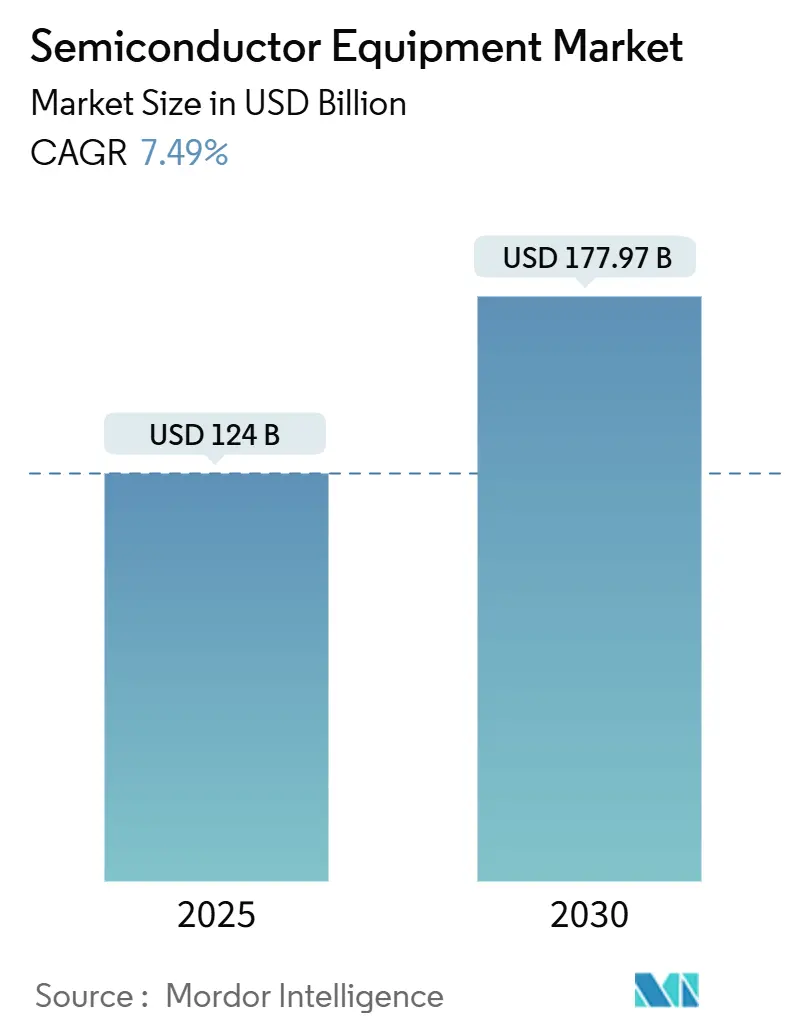
| Market Size (2025) | USD 124 Billion |
| Market Size (2030) | USD 177.97 Billion |
| Growth Rate (2025 - 2030) | 7.49% CAGR |
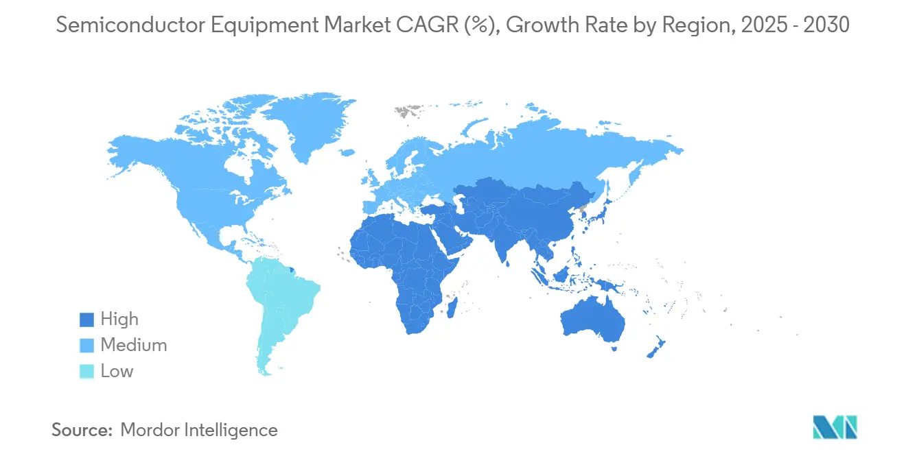
| Fastest Growing Market | Middle East and Africa |
| Largest Market | Asia-Pacific |
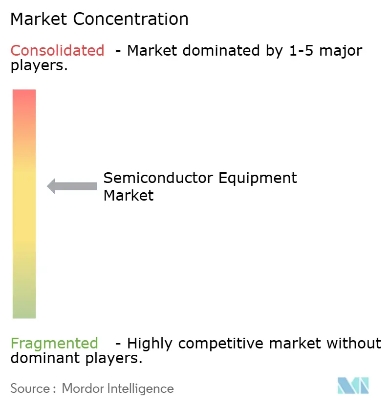
| Market Concentration | Medium |
Major Players*Disclaimer: Major Players sorted in no particular order Image © Mordor Intelligence. Reuse requires attribution under CC BY 4.0. |
|

Semiconductor Equipment Market Analysis by Mordor Intelligence
The semiconductor equipment market size was valued at USD 124.00 billion in 2025 and is forecast to reach USD 177.97 billion by 2030, at a 7.49% CAGR. Robust fab construction, record equipment backlogs, and a wave of government incentives underpin this trajectory. Foundries are accelerating capacity at 2 nm and below, while Outsourced Semiconductor Assembly and Test (OSAT) players scale advanced-package lines to serve artificial-intelligence (AI) demand. Geopolitical efforts to achieve technological sovereignty are shaping capital-spending patterns, forcing tool vendors to juggle export controls in China with subsidy-fuelled opportunities in North America, Europe, and the Middle East. Equipment makers that bundle process breadth, software analytics, and service coverage are securing multi-year purchase commitments from the sector’s largest investors.
Key Report Takeaways
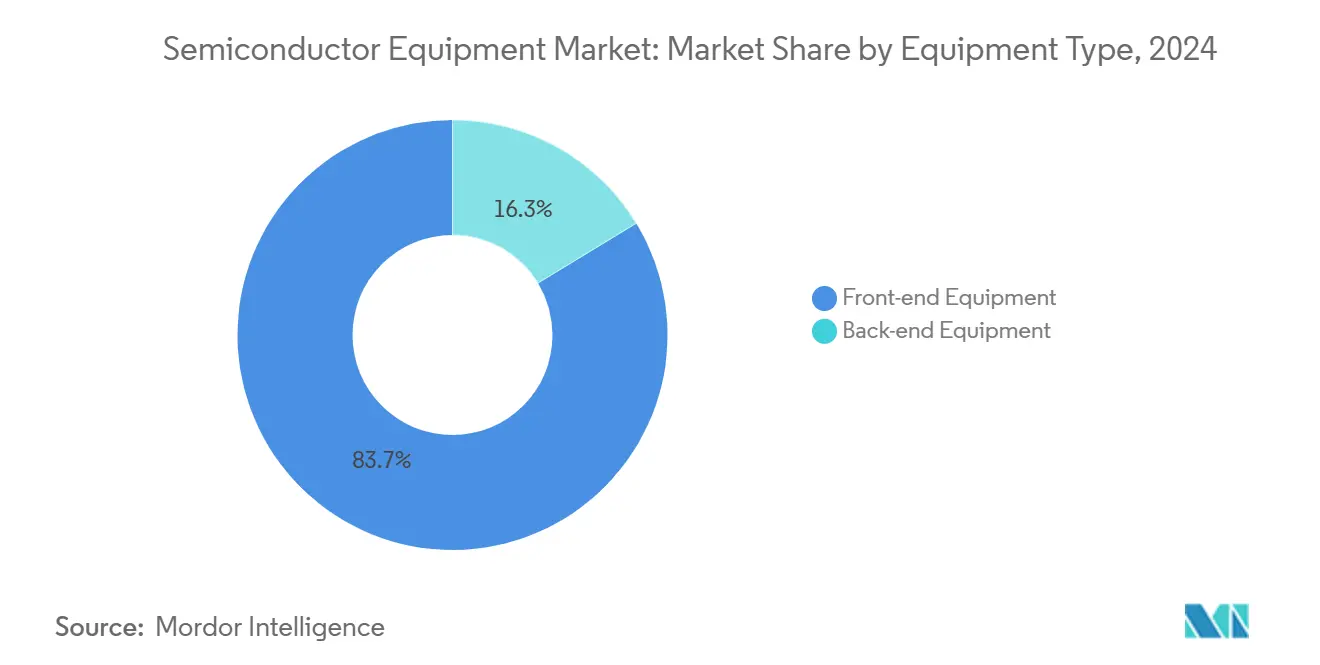
- By equipment type, front-end wafer-processing tools commanded 83.7% of the semiconductor equipment market share in 2024; High-NA EUV systems are projected to expand at a 21.1% CAGR through 2030.
- By supply-chain participant, foundries led with 52.2% revenue share in 2024, while OSAT providers are advancing at a 12.2% CAGR to 2030.
- By wafer size, 300 mm tools accounted for 62.2% of the semiconductor equipment market size in 2024; ≤150 mm SiC/GaN power-wafer tools are growing at 11.1% CAGR.
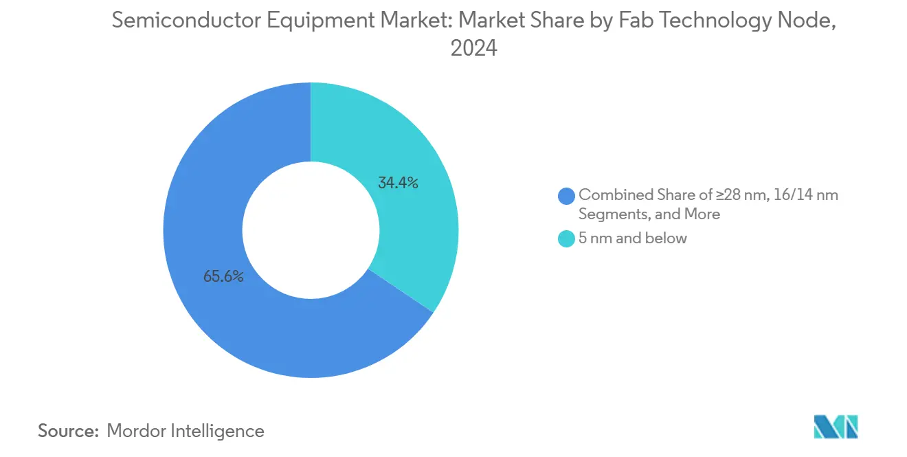
- By technology node, 5 nm-and-below processes held 34.4% share of the semiconductor equipment market size in 2024, whereas 2 nm-and-below tools exhibit a 21.5% CAGR outlook.
- By end-user industry, computing and data-center applications captured 29.9% of the semiconductor equipment market share in 2024; automotive and mobility remain the fastest-growing end-market with a 13.8% CAGR to 2030.
- By geography, Asia-Pacific retained 72% semiconductor equipment market share in 2024, whereas the Middle East and Africa market is expanding at a 9.9% CAGR.
Global Semiconductor Equipment Market Trends and Insights
Drivers Impact Analysis
| Driver | (~) % Impact on CAGR Forecast | Geographic Relevance | Impact Timeline |
|---|---|---|---|
| Surging demand for advanced consumer electronics and smartphones | +1.4% | Global, with a concentration in Asia-Pacific | Medium term (2-4 years) |
| Rapid AI-, IoT- and edge-device node investments | +1.8% | North America, Asia-Pacific, Europe | Long term (≥ 4 years) |
| Government subsidy waves (CHIPS, EU Chips Act, etc.), boosting the tool CAPEX | +1.6% | North America, Europe, Asia-Pacific | Medium term (2-4 years) |
| Transition to GAA and High-NA EUV necessitates new toolsets | +1.2% | Asia-Pacific, North America | Long term (≥ 4 years) |
| Sustainability mandates driving "green fab" retrofit tools | +0.7% | Europe, North America, Asia-Pacific | Medium term (2-4 years) |
| 3D heterogeneous-integration packaging demand spike | +0.5% | Global | Medium term (2-4 years) |
Source: Mordor Intelligence
Surging demand for advanced consumer electronics and smartphones
Smartphones, wearables, and mixed-reality devices keep adding logic, memory, and analog content that must be built at ever-smaller nodes, pushing foundries to accelerate capacity on 28 nm–7 nm lines.[1]Taiwan Semiconductor Manufacturing Company, “2 nm Technology,” tsmc.com Advanced packaging that miniaturizes high-bandwidth functions without raising power budgets drove a sizable share of early-2025 revenue, triggering an upgrade wave in bumping, test, and lithography equipment. Heterogeneous-integration lines stacking chiplets vertically are expanding at double-digit rates, lifting shipments of flip-chip bonders and wafer-level inspection tools. Tool makers offering modular deposition chambers with rapid recipe switching are winning orders as consumer-product cycles tighten. Strong handset refresh rates across India and Southeast Asia keep mature-node tools running near full utilization, proving that resilient billings are achievable even during premium-device launches.
Rapid AI-, IoT- and edge-device node investments
Data-center operators seek chips that offer higher TOPS-per-watt, boosting procurement of extreme ultraviolet (EUV) scanners and atomic-layer deposition modules used at 3 nm and below. AI accelerator start-ups in the United States and Europe are signing capacity reservation agreements that tie multi-year HBM purchases to guaranteed access to leading-edge lithography, shifting demand risk from chip designers to equipment makers. Edge AI devices for factory automation and smart-city deployments accelerate 16 nm–12 nm demand, spurring fresh orders for 300 mm etch systems tailored to embedded non-volatile memory. Tool suppliers deploy AI in situ process-monitoring algorithms, shortening recipe-development cycles and improving chamber uptime. The self-reinforcing loop between AI workload growth and smarter tools bolsters the semiconductor equipment market well past 2030.
Government subsidy waves are boosting the tool CAPEX
The United States CHIPS and Science Act, the European Chips Act, and comparable Asian funds are underwriting at least 18 fab ground-breakings in 2025. Tax credits slash payback times for lithography, chemical-vapor-deposition (CVD), and metrology assets, prompting IDMs to green-light capacity that pure economics once made marginal. Equipment providers are tailoring service contracts and spare-part depots to regional support requirements embedded in grant agreements. National security clauses often mandate local sourcing of subsystems such as vacuum pumps and positioning stages, giving rise to micro-supply chains near new fabs in Texas, Saxony, and Kumamoto. Subsidies are also steering tool development toward lower-carbon footprints, helping vendors secure procurement preference lists tied to greenhouse-gas reduction benchmarks.
Transition to GAA and High-NA EUV necessitates new toolsets
Gate-all-around (GAA) nanosheet transistors introduce vertical channel structures that demand sub-angstrom control in epitaxy, spacer deposition, and selective wet cleaning. High-NA EUV lithography slices exposure footprints by 70%, but requires reticle-handling, contamination-control, and resist-processing equipment newly certified for tighter overlay budgets. Early tool shipments to Albany NanoTech and leading foundry pilot lines have triggered follow-on metrology demand, especially for 3-D atomic-force and optical scatterometry systems. Suppliers of dielectric deposition systems are redesigning hardware to accommodate the thermal budget constraints of GAA stacks. The interplay of novel materials and extreme numerical-aperture optics establishes a multiyear equipment refresh cycle that favors vendors with deep subsystem integration know-how.
Restraints Impact Analysis
| Restraint | (~) % Impact on CAGR Forecast | Geographic Relevance | Impact Timeline |
|---|---|---|---|
| Extremely high CAPEX and long pay-back cycles | -1.1% | Global | Long term (≥ 4 years) |
| Specialty-material supply bottlenecks are delaying tool shipments | -0.8% | Global, with acute impact in North America and Europe | Short term (≤ 2 years) |
| Export-control restrictions on China-bound tools | -0.4% | China, with implications for global supply chains | Medium term (2-4 years) |
| Acute shortage of skilled field-service engineers | -0.6% | Global, particularly North America | Medium term (2-4 years) |
Source: Mordor Intelligence
Extremely high CAPEX and long pay-back cycles
A single advanced-logic fab now costs well above USD 20 billion, making the customer base for leading-edge tools increasingly concentrated. Lengthy depreciation periods stretch procurement scrutiny, compelling toolmakers to demonstrate multi-node extendibility before purchase orders are released. Vendors respond with upgrade-ready platforms, modular vacuum geometries, and subscription-based process-control software that spreads cost over a tool’s life span. Some IDMs delay capacity expansions, which defers installations and shifts revenue recognition to late project phases. Nevertheless, the relentless need for performance-per-watt keeps road maps intact, limiting the overall drag on the semiconductor equipment market.
Specialty-material supply bottlenecks are delaying tool shipments
Gallium, germanium, and other high-purity compounds face export restrictions that elongate tool-building lead times beyond 12 months. Shortages of extreme-vacuum valves and electrostatic chucks add complexity for suppliers of etch and deposition platforms. Some vendors have launched dual-source strategies, qualifying non-Chinese alternatives for rare-earth magnets used in stepper stages. Others build buffer inventories to cover six-month production windows, tying up working capital and raising unit costs. Although governments are financing new rare-earth processing plants, commercial supply will trail demand through at least 2027, weighing on the semiconductor equipment industry’s near-term delivery cadence.
Segment Analysis
By Equipment Type: High-NA EUV Drives Premium Tool Demand
Front-end wafer-processing instruments captured 83.7% of the semiconductor equipment market share in 2024, underscoring the central role of lithography, etch, and deposition in yield improvement. Within this segment, High-NA EUV scanners post a 21.1% CAGR to 2030 because they are indispensable for patterning 2 nm logic and 3-D DRAM structures; multi-system orders from fabs in Taiwan and New York already total several billion USD.[2]Center for Strategic and International Studies, “Albany NanoTech’s Potential to Support the National Semiconductor Technology Center,” csis.org
Backend complexity fuels innovations such as thermo-compression bonders with sub-2 µm alignment accuracy and fan-out wafer-level packaging that leverages front-end lithographic precision. Vendors that combine lithography optics, placement robotics, and high-frequency test modules into unified platforms are capturing a growing share of advanced-package budgets, extending lithography-grade investments further down the supply chain.
Note: Segment shares of all individual segments available upon report purchase
By Supply-Chain Participant: Foundries Lead Capacity Expansion
Foundries accounted for 52.2% of semiconductor equipment market revenue in 2024 as fabless chip firms concentrate orders on TSMC, Samsung Foundry, and GlobalFoundries. Mega-projects in Arizona, Dresden, and Kaohsiung each feature clusters of EUV scanners, multi-chamber etch stacks, and atomic-layer deposition tools configured for rapid recipe swaps, reflecting the foundry model’s need to host diverse customer process flows. Strict uptime commitments drive bundled service contracts that now equal 25–30% of tool acquisition value, creating annuity streams for equipment suppliers.
OSAT houses emerge as the fastest-growing customer category at a 12.2% CAGR, propelled by 2.5-D and 3-D package architectures required for AI accelerators and automotive domain controllers. New capex lines include laser-drilling for through-silicon vias, high-density flip-chip bonders, and molded-underfill dispense systems. Integrated device manufacturers (IDMs) retain a sizeable but declining share as they pursue fab-lite strategies that outsource leading-edge logic while investing selectively in power, analog, and sensor lines.
By Wafer Size: 300 mm Dominates While SiC/GaN Spurs Niche Tool Orders
The 300 mm node retained 62.2% semiconductor equipment market share in 2024, supported by record fab utilizations and new green-field projects in the United States, Japan, and Singapore. SEMI projects global 300 mm capacity to exceed 10 million wafer starts per month in 2025, sustaining brisk demand for batch-production etchers, CMP units, and automated material-handling systems. Yield-critical process-control tools that monitor defectivity across the larger surface area now command premium pricing.
Smaller-diameter tools are experiencing a renaissance as silicon-carbide (SiC) and gallium-nitride (GaN) power devices move toward 150 mm and, in select pilot lines, 300 mm production. ≤150 mm SiC/GaN equipment is advancing at 11.1% CAGR, led by high-temperature epitaxy reactors and ultra-clean implant systems. Infineon’s demonstration of 300 mm GaN wafers signals a future crossover where specialty-material fabs adopt mainstream automation platforms, opening a fresh opportunity set for tool suppliers attuned to wide-bandgap process requirements.
By Fab Technology Node: 2 nm and Below Ignites New Equipment Cycles
Logic at 5 nm and below captured 34.4% share of the semiconductor equipment market size in 2024, and the ramp to 2 nm is driving a 21.5% CAGR for the sub-2 nm tool segment. TSMC plans to start high-volume 2 nm production in late 2025, blending nanosheet transistors with backside power delivery to slash resistance losses. The node demands quadruple-pattern EUV, atomic-layer etch, and cryogenic ion implantation—all areas where only a handful of vendors qualify. Foundries hedge risk by ordering overlapping tool generations, keeping 3 nm lines warm for volume products while pilot-running 2 nm, thereby enlarging total addressable spend.
Mature nodes such as 28 nm remain vital for display drivers, microcontrollers, and analog ICs, supporting steady bookings for i-line steppers and wet-bench cleans. Specialty lithography road-maps track automotive quality-control standards, ensuring demand diversity across the entire node spectrum and stabilizing the semiconductor equipment market against isolated node slowdowns.
Note: Segment shares of all individual segments available upon report purchase
By End-User Industry: AI Accelerates Computing Segment Growth
Computing and data-center customers consumed 29.9% of semiconductor equipment market revenue in 2024, reflecting the insatiable need for graphics processing units (GPUs) and AI accelerators. Hyperscale operators pre-purchase capacity slots at 2 nm and negotiate direct wafer allocation with foundries, effectively pulling equipment shipments forward. High-bandwidth-memory demand forces upgrades in flip-chip ball-grid-array assembly lines and X-ray inspection tools that guarantee interposer reliability.
Automotive and mobility applications lead growth with a 13.8% CAGR through 2030 as electric-vehicle inverters, battery-management ICs, and advanced-driver-assistance systems (ADAS) proliferate. Wide-bandgap power devices rely on 150 mm–200 mm SiC epitaxial reactors, while radar and LiDAR modules stimulate orders for compound-semiconductor deposition and etch tools. Communications infrastructure continues to absorb RF-front-end and millimeter-wave device capacity, sustaining lithography and metrology demand at 28 nm–14 nm nodes. Consumer electronics maintains volume shipments at sub-10 nm nodes for flagship mobile SoCs, whereas industrial IoT drives incremental demand for ruggedized microcontrollers built on 40 nm platforms.
Geography Analysis
Asia-Pacific retained 72.2% semiconductor equipment market share in 2024, powered by dense ecosystems in Taiwan, South Korea, and mainland China; Taiwan’s foundry cluster alone ran above 90% utilization, sustaining EUV and metrology orders.[3]Pamir LLC, “Asia is set to power the global semiconductor market,” pamirllc.com South Korea intensified spending on 1-beta DRAM and gate-all-around logic, while China’s drive for self-reliance lifted domestic etcher and deposition installations even under export-control pressure.
North America’s renaissance stems from CHIPS Act grants; Albany NanoTech took delivery of the world’s first High-NA EUV tool, creating a cornerstone for a domestic lithography ecosystem. Simultaneous investments by TSMC and Intel in Arizona form a corridor stretching from equipment assembly in Oregon to materials supply in Texas, re-balancing regional demand.
Europe sharpened its specialty-technology focus—automotive power devices, RF front-ends, and advanced sensors—using the European Chips Act to target a doubling of regional capacity by 2030; Saxony’s dual 300 mm lines already combine logic, analog, and power processing.
The Middle East and Africa logged the fastest growth at 9.9% CAGR, fuelled by Saudi Arabia’s USD 9 billion fab plan and UAE feasibility studies, which require turnkey tool-support contracts spanning training, refurbishment, and logistics. South America remains niche; Brazil is investing selectively in automotive and industrial chips that rely on mature-node 200 mm tools.
Competitive Landscape
The five largest equipment suppliers hold a significant share of global revenue, a moderate concentration built on proprietary lithography optics, vacuum science, and vast patents. Tokyo Electron’s pledge to invest JPY 1.5 trillion (USD 10 billion) in R&D across five years signals a platform-integration strategy that binds hardware, software, and services into long-term agreements. ASML preserves near-monopoly status in EUV yet broadens into High-NA analytics and stochastic-defect mitigation as Chinese competitors target mature-node lithography.
White-space opportunities cluster around wide-bandgap materials and advanced packaging: Infineon’s 300 mm GaN breakthrough expands demand for epi reactors, MOCVD sources, and high-temperature anneal furnaces.[4]Infineon Technologies, “Infineon 2025 Predictions – Gallium Nitride (GaN),” infineon.com Backend specialists develop copper-clip attach lines and warpage-control ovens optimized for chiplet packages, while Chinese vendors leverage policy support and aggressive pricing to gain domestic etch and wet-clean share.
Export-control scrutiny heightens strategic risk; U.S. legislators have asked tool makers to detail China revenue, prompting firms to craft dual-compliance product lines that balance market access with regulatory limits.
Semiconductor Equipment Industry Leaders
-
ASML Holding NV
-
Applied Materials Inc.
-
Lam Research Corp.
-
Tokyo Electron Ltd.
-
KLA Corp.
- *Disclaimer: Major Players sorted in no particular order
Recent Industry Developments
- May 2025: TSMC confirmed volume production of 2 nm N2 logic in late 2025, introducing nanosheet transistors with backside power delivery.
- May 2025: Qualcomm and HUMAIN agreed to build AI data centers and a design hub in Saudi Arabia, creating fresh equipment demand for leading-edge logic and advanced packaging.
- April 2025: SEMI reported 2.2% YoY growth in worldwide silicon-wafer shipments, with 300 mm slices up 6% YoY, underscoring sustained equipment utilization.
- March 2025: Albany NanoTech became the first National Semiconductor Technology Center site for EUV lithography, backed by USD 825 million federal and USD 1 billion state funds.
Global Semiconductor Equipment Market Report Scope
A semiconductor is an essential electronic equipment component, enabling advances in telecommunications, computing, biotechnology, weapon technology, aviation, renewable energy, and various other industries. Semiconductors, also known as integrated circuits (ICs) or microchips, are made from pure materials, such as silicon and germanium, and composite materials, such as gallium arsenide.
The scope of the study for the semiconductor equipment market is structured to track the spending on equipment types, i.e., front-end and back-end equipment. The market is further segmented into supply chain participants, i.e., IDM, OSAT, and foundry. The market is also segmented by geography. All the data presented in this study is as per recent information. All the market projections are adjusted to reflect the impact of COVID-19 on the semiconductor equipment market. The market sizes and forecasts are provided in terms of value (USD billion) for all the above segments.
| By Equipment Type | Front-end Equipment | Lithography Equipment | ||
| Etch Equipment | ||||
| Deposition Equipment | ||||
| Metrology / Inspection Equipment | ||||
| Cleaning Equipment | ||||
| Photoresist Processing Equipment | ||||
| Other Front-end Types | ||||
| Back-end Equipment | Test Equipment | |||
| Assembly and Packaging Equipment | ||||
| By Supply-Chain Participant | IDM | |||
| Foundry | ||||
| OSAT | ||||
| By Wafer Size | 300 mm | |||
| 200 mm | ||||
| ≤150 mm | ||||
| By Fab Technology Node | ≥28 nm | |||
| 16/14 nm | ||||
| 10/7 nm | ||||
| 5 nm and below | ||||
| By End-user Industry | Computing and Data-Center | |||
| Communications (5G, RF) | ||||
| Automotive and Mobility | ||||
| Consumer Electronics | ||||
| Industrial and Others | ||||
| By Geography | North America | United States | ||
| Canada | ||||
| Mexico | ||||
| South America | Brazil | |||
| Argentina | ||||
| Rest of South America | ||||
| Europe | Germany | |||
| United Kingdom | ||||
| France | ||||
| Italy | ||||
| Spain | ||||
| Rest of Europe | ||||
| Asia-Pacific | China | |||
| Japan | ||||
| South Korea | ||||
| India | ||||
| Rest of Asia-Pacific | ||||
| Middle East and Africa | Middle East | Saudi Arabia | ||
| United Arab Emirates | ||||
| Turkey | ||||
| Rest of Middle East | ||||
| Africa | South Africa | |||
| Nigeria | ||||
| Egypt | ||||
| Rest of Africa | ||||
| Front-end Equipment | Lithography Equipment |
| Etch Equipment | |
| Deposition Equipment | |
| Metrology / Inspection Equipment | |
| Cleaning Equipment | |
| Photoresist Processing Equipment | |
| Other Front-end Types | |
| Back-end Equipment | Test Equipment |
| Assembly and Packaging Equipment |
| IDM |
| Foundry |
| OSAT |
| 300 mm |
| 200 mm |
| ≤150 mm |
| ≥28 nm |
| 16/14 nm |
| 10/7 nm |
| 5 nm and below |
| Computing and Data-Center |
| Communications (5G, RF) |
| Automotive and Mobility |
| Consumer Electronics |
| Industrial and Others |
| North America | United States | ||
| Canada | |||
| Mexico | |||
| South America | Brazil | ||
| Argentina | |||
| Rest of South America | |||
| Europe | Germany | ||
| United Kingdom | |||
| France | |||
| Italy | |||
| Spain | |||
| Rest of Europe | |||
| Asia-Pacific | China | ||
| Japan | |||
| South Korea | |||
| India | |||
| Rest of Asia-Pacific | |||
| Middle East and Africa | Middle East | Saudi Arabia | |
| United Arab Emirates | |||
| Turkey | |||
| Rest of Middle East | |||
| Africa | South Africa | ||
| Nigeria | |||
| Egypt | |||
| Rest of Africa | |||
Key Questions Answered in the Report
What is driving the current growth of the semiconductor equipment market?
Surging AI workloads, government semiconductor incentives, and foundry expansions at 3 nm and below are the primary growth catalysts, lifting global equipment billings toward USD 170 billion by 2030.
Why are High-NA EUV tools considered critical for next-generation chips?
High-NA EUV scanners enable sub-2 nm patterning with tighter line-edge control, making them essential for the performance gains promised by nanosheet transistors and backside power delivery.
How are government subsidies affecting tool spending patterns?
Programs such as the CHIPS Act and the European Chips Act shorten payback times, accelerate fab timelines, and localize supply chains, leading to concentrated regional surges in equipment orders.
Which end market is growing fastest for semiconductor equipment?
The automotive and mobility segment shows the highest CAGR at 13.8% through 2030, propelled by electric-vehicle power electronics and advanced driver-assistance semiconductors.
What challenges could dampen equipment market growth over the next five years?
Multi-billion-dollar fab costs, specialty-material shortages, and stricter export controls can delay tool installations and lengthen ROI periods, tempering otherwise strong demand.
Page last updated on: June 26, 2025

