Semiconductor Bonding Market Size and Share
Market Overview
| Study Period | 2021 - 2031 |
|---|---|
| Market Size (2026) | USD 1.19 Billion |
| Market Size (2031) | USD 1.45 Billion |
| Growth Rate (2026 - 2031) | 4.04% CAGR |
| Fastest Growing Market | Asia-Pacific |
| Largest Market | Asia-Pacific |
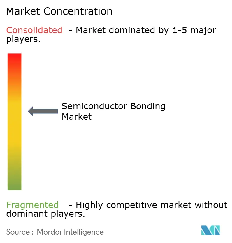
| Market Concentration | Medium |
Major Players *Disclaimer: Major Players sorted in no particular order Image © Mordor Intelligence. Reuse requires attribution under CC BY 4.0. | |
Semiconductor Bonding Market Analysis by Mordor Intelligence
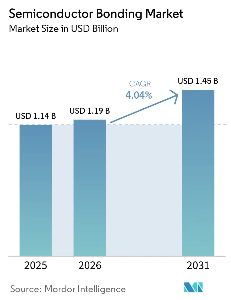
The Semiconductor Bonding Market size is expected to grow from USD 1.14 billion in 2025 to USD 1.19 billion in 2026 and is forecast to reach USD 1.45 billion by 2031 at 4.04% CAGR over 2026-2031. Government subsidies, chiplet architectures, and 3D integration are reshaping capital-spending priorities, moving bonding demand away from traditional fab cycles and toward advanced-packaging lines in Asia-Pacific, North America, and Europe. Die-to-die bonding already captures 53.91% of interconnect-level revenue because heterogeneous integration delivers higher yield and faster time-to-market than monolithic SoCs. Equipment makers that combine plasma activation, inline metrology, and thermocompression within a single cluster tool shorten cycle time by 40%, raising tool utilization above 70% and accelerating payback for outsourced assembly and test providers. Subsidy races in the United States, the European Union, South Korea, and Japan now channel more than USD 80 billion toward bonding capacity, decoupling equipment demand from lithography investment and softening exposure to front-end node delays.
Key Report Takeaways
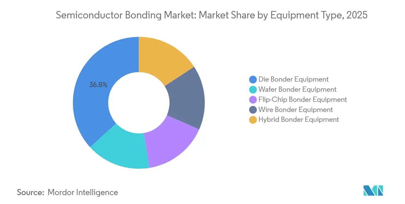
- By equipment type, die bonder equipment captured 36.77% of the Semiconductor Bonding market share in 2025; hybrid bonder equipment is projected to rise at a 4.27% CAGR through 2031.
- By interconnect level, die-to-die bonding accounted for 53.91% share of the Semiconductor Bonding market size in 2025, whereas wafer-to-wafer bonding is on course for a 4.52% CAGR to 2031.
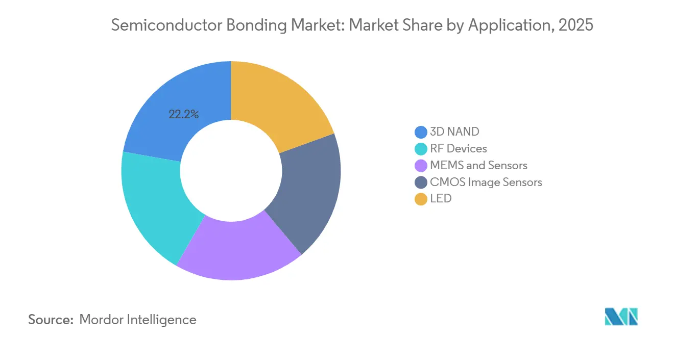
- By application, 3D NAND commanded 22.21% of the Semiconductor Bonding market size in 2025, while CMOS image sensors are set to expand at a 4.67% CAGR during 2026-2031.
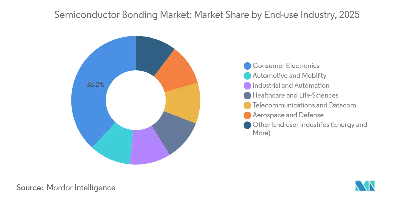
- By end-use industry, consumer electronics led with 38.23% revenue share in 2025; automotive and mobility is forecast to post the fastest 5.01% CAGR through 2031.
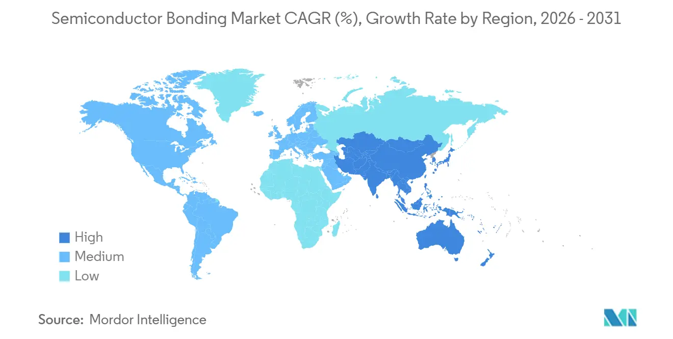
- By geography, Asia-Pacific contributed 41.53% to 2025 revenue and is projected to advance at a 4.91% CAGR to 2031.
Note: Market size and forecast figures in this report are generated using Mordor Intelligence’s proprietary estimation framework, updated with the latest available data and insights as of January 2026.
Global Semiconductor Bonding Market Trends and Insights
Drivers Impact Analysis*
| Driver | (~) % Impact on CAGR Forecast | Geographic Relevance | Impact Timeline |
|---|---|---|---|
| Growing demand for advanced packaging and miniaturization | +1.2% | Global, APAC core with 60% of capacity additions | Medium term (2-4 years) |
| Expansion of consumer electronics and automotive sectors | +0.9% | APAC (consumer), North America & Europe (automotive) | Short term (≤ 2 years) |
| Rising adoption of 3D integration and MEMS devices | +0.8% | APAC manufacturing hubs, North America design centers, Europe industrial automation | Medium term (2-4 years) |
| AI-driven heterogeneous integration for edge computing | +0.7% | Global, led by North America hyperscalers and APAC foundries | Long term (≥ 4 years) |
| Government semiconductor subsidy races | +0.5% | North America, Europe, South Korea, Japan, Taiwan | Long term (≥ 4 years) |
| Source: Mordor Intelligence | |||
Growing Demand for Advanced Packaging and Miniaturization
Heterogeneous chiplets allow foundries to stack logic, memory, and analog dies at sub-10 micrometer pitches, removing micro-bumps and lowering parasitic capacitance by 80%[1]TSMC Technology Symposium, “SoIC Roadmap,” tsmc.com. UCIe 3.0 enables 64 GT/s links, giving AI accelerators up to 4 TB/s bandwidth per square millimeter. Intel Foveros Direct reaches 15 times the interconnect density of flip-chip packaging, supporting 300 W thermal-design envelopes for datacenter tiles. Glass substrates enter pilot production with 10-times lower warpage than organic materials and cut panel-level cost by 30%. As a result, the semiconductor bonding market attracts record orders for hybrid bonders that integrate plasma activation, alignment, and thermocompression in one tool cluster.
Expansion of Consumer Electronics and Automotive Sectors
Wafer-level chip-scale packaging shrinks CMOS (Complementary Metal-Oxide-Semiconductor) image-sensor height by 40%, enabling thinner phones and multi-camera vehicles. Automotive CIS shipments are projected to hit 1.2 billion units by 2029, equivalent to USD 8.4 billion in revenue. Silicon carbide traction inverters need die-attach that survives 200°C, pushing adoption of sintered silver past 50% share in new EV platforms. Copper wire already represents 38% of automotive bonds and will pass 45% by 2027 as AEC-Q006 processes mature. These trends expand the market by drawing high-power and optical modules into advanced-packaging flows.
Rising Adoption of 3D Integration and MEMS Devices
Samsung V10 NAND stacks 420-plus layers using wafer-to-wafer hybrid bonding that demands surface roughness below 5 nm. Kioxia BiCS8 moves peripheral logic beneath 332-layer memory arrays, boosting per-die density to 2 Tbit. MEMS inertial sensors achieve leak rates under 1×10⁻¹¹ mbar·L/s with gold-indium bonding at 280°C, lowering per-unit cost by 40% versus die-level capping. Plasma-activated direct bonding removes adhesives, raises bond strength above 20 MPa, and enters mass production for pressure sensors in industrial automation. Together, these moves enlarge the semiconductor bonding market by opening new vertical-stack architectures.
AI-Driven Heterogeneous Integration for Edge Computing
Co-packaged optics hybrid-bond silicon-photonics dies to switch ASICs (Application-Specific Integrated Circuits) at 5 µm pitch, cutting latency by 60% for 800G Ethernet[2]Intel Newsroom, “Foveros Direct Technology Brief,” intel.com. UCIe chiplet ecosystems allow hyperscalers to select best-in-class tiles across foundries, improving yield by 40% on die sizes above 600 mm². Thermal-compression bonding at 300°C replaces mass reflow for HBM4 stacks, enabling void-free joints below 40 µm pitch. Fan-out wafer-level packages integrate LPDDR5X in foldable phones and drop package thickness by 30%. These breakthroughs lift the market by merging optical, logic, and memory elements within sub-5 W envelopes.
Restraints Impact Analysis*
| Restraint | (~) % Impact on CAGR Forecast | Geographic Relevance | Impact Timeline |
|---|---|---|---|
| High capital investment and operational costs | -0.6% | Global, more acute in North America & Europe | Short term (≤ 2 years) |
| Process complexity at advanced nodes | -0.4% | APAC foundries and OSATs | Medium term (2-4 years) |
| Limited availability of ultra-flat wafers for hybrid bonding | -0.3% | Global supply chain, concentrated in Japan & Taiwan | Medium term (2-4 years) |
| Source: Mordor Intelligence | |||
High Capital Investment and Operational Costs
Hybrid-bonding tools cost USD 5-8 million each, and a full line tops USD 30 million, straining OSAT (Outsourced Semiconductor Assembly and Test) margins that average 10%. Early utilization stays near 50% because design rules evolve alongside customer qualifications, stretching payback beyond three years. Labor in the United States and Europe is 40-50% pricier than in Asia, and CMP consumables run USD 15-20 per wafer, triple flip-chip underfill expense, pressuring opex. These factors temper near-term expansion of the semiconductor bonding market.
Process Complexity at Advanced Nodes
Sub-3 nm logic requires less than 1 µm pitch and 200 nm alignment tolerance; plasma activation must remove oxides without harming low-k dielectrics within a ±5°C window. Void formation cuts thermal conductivity by 30% and escapes acoustic detection below 10 µm in size. HBM4 stacks scrap entirely if one die misaligns, erasing cost gains at yields below 95%. Extra on-chip test circuits occupy up to 12% die area, adding mask costs. High complexity flattens the semiconductor bonding market growth curve.
*Our forecasts treat driver/restraint impacts as directional, not additive. The impact forecasts reflect baseline growth, mix effects, and variable interactions.
Segment Analysis
By Equipment Type: Hybrid Bonding Pulls Investment Despite Die Bonder Dominance
Die Bonder Equipment retained 36.77% of 2025 revenue as high-precision eutectic and epoxy attach remain core for power and RF components. Flip-chip bonders address 40-150 µm pitches at volumes over 5,000 units per hour, while wire bonders dominate cost-sensitive assemblies. Wafer bonders enable MEMS and 3D NAND with 30-40% cost savings over die-level capping, anchoring the semiconductor bonding market size for legacy devices.
Hybrid bonders will post the quickest 4.27% CAGR through 2031 because HBM4, chiplets, and co-packaged optics require less than 10 µm pitches. EV Group’s GEMINI platform applies 350 kN forces for flux-free bonding, and the Applied–Besi Kinex cluster cuts cycle time by 40%. TSMC’s CoWoS ramp consumed about 250 tools valued at nearly USD 1.5 billion, confirming capital appetite. The market reallocates spend toward hybrid cluster tools even while die-attach lines run at high utilization.


By Interconnect Level: Die-to-Die Captures Chiplet Wave
Die-to-die bonding controlled 53.91% of 2025 revenue because UCIe standards lift bandwidth to 4 TB/s mm², letting AI accelerators pair logic with HBM4 tiles. Intel EMIB connects dies at 55 µm pitch without full interposers, and Amkor now offers EMIB in Arizona and Korea. This topology anchors 2026-2029 roadmaps and secures the largest semiconductor bonding market share.
Wafer-to-wafer hybrid bonding is projected to grow at 4.52% CAGR during the forecast period (2026-2031) as 3D NAND sails past 400 layers and targets 1,000-layer stacks. Samsung, YMTC, and Kioxia all bond CMOS logic under memory at the wafer level, improving yield by 25%. Die-to-wafer bonding supports CIS and RF devices where known-good dies mount onto passive wafers. These combined flows reinforce the semiconductor bonding market breadth across memory, logic, and sensor nodes.
By Application: CMOS Image Sensors Accelerate on Automotive Demand
3D NAND already supplies 22.21% of 2025 revenue, and hybrid bonding remains the only interface that reaches inside 400-plus-layer stacks. MEMS inertial and pressure sensors adopt hermetic wafer bonding, while RF front-ends rely on flip-chip GaN dies on copper–tungsten carriers for mmWave. LED micro-arrays use laser-assisted bonding to attach 25,600 dies in adaptive headlights, widening semiconductor bonding industry exposure to diversified optoelectronics.
CMOS image sensors are set to expand at 4.67% CAGR to 2031, driven by multi-camera ADAS (Advanced Driver Assistance Systems) that integrates 8-12 modules per vehicle and pushes resolution from 2 MP to 8 MP. Wafer-level TSV packages shrink height by 40% and boost thermal performance, uplifting the semiconductor bonding market size in optical segments.
By End-use Industry: Automotive Electrification Outpaces Consumer Electronics
Consumer electronics still delivered 38.23% of 2025 revenue on smartphone cameras, wearables, and earbuds using fan-out wafer-level packages. Industrial automation depends on hermetic MEMS (Micro-Electro-Mechanical Systems), telecom needs co-packaged optics, and healthcare implants use gold–tin eutectic attach. Aerospace keeps wire bonding for radiation tolerance. These diverse verticals insulate the semiconductor bonding market against single-segment slumps while automotive leads growth.
Automotive and mobility will post a 5.01% CAGR through 2031 because silicon-carbide inverters need sintered-silver attach that withstands 800-V drivetrains. Copper wire bonding will cross 45% of automotive assemblies by 2027, and wafer-level CIS adoption cuts module height for slim A-pillars. MEMS mirror LiDAR (Light Detection and Ranging) modules rely on fluxless thermocompression, cementing the sector’s pull on the semiconductor bonding market.
Geography Analysis
Asia-Pacific generated 41.53% of 2025 revenue and is forecast to grow 4.91% CAGR through 2031, the highest regional pace. TSMC raised CoWoS capacity from 12,000 to 50,000 wafers per month by 2026 and broke ground on a Chiayi fab aimed at AI accelerators. South Korea’s USD 230 billion plan funds Samsung Yongin and SK Hynix P&T7, tripling domestic HBM output by 2028. China’s XTacking 232-layer NAND avoids restricted tools, while Japan funnels JPY 1.5 trillion (USD 9.3 billion) into Tokyo Electron research and development. Regional supply concentration feeds the semiconductor bonding market by pooling skilled labor, suppliers, and subsidies.
North America benefits from USD 36.4 billion CHIPS Act grants, with Amkor’s Arizona plant and SK Hynix’s Indiana HBM line anchoring advanced-packaging capacity. Intel outsources EMIB packaging to Amkor, and Micron paid USD 1.8 billion for PSMC’s P5 fab to expand DRAM volume. Mexico draws nearshoring wire-bonding jobs at 60% lower labor cost, trimming logistics times to Texas fabs by 40%. The policy focuses on packaging, versus lithography, and positions the market for resilient North American growth.
Europe secured EUR 43 billion (USD 48.62 billion) under IPCEI-ME, with EUR 2.5 billion (USD 2.83 billion) for NanoIC hybrid-bonding kits. TSMC commits EUR 10 billion (USD 11.31 billion) for a 300 mm fab in Dresden, starting 2027, and Intel’s Magdeburg site targets initial output by 2029. Although timelines extend 18-24 months longer than in Asia due to permitting, the capital inflow enlarges local bonding demand. South America remains legacy-focused, and Middle East projects are exploratory. Net impact keeps the semiconductor bonding market concentrated in Asia yet diversifies geopolitical footprints.

Competitive Landscape
The Semiconductor Bonding market is moderately concentrated. Export controls split the market: Chinese OSATs depend on domestic die-attach and wire bonders from HANMI and Shinkawa that cost 30% less but lack the less than 5 µm alignment needed for hybrid bonding. Overall, the semiconductor bonding market shows moderate concentration, shaped by IP races around alignment metrology and plasma chemistry.
Semiconductor Bonding Industry Leaders
ASMPT
Besi
Kulicke and Soffa Industries, Inc.
Applied Materials, Inc.
Tokyo Electron Limited
- *Disclaimer: Major Players sorted in no particular order

Recent Industry Developments
- March 2026: Adeia Inc. announced that it has expanded and renewed its intellectual property (IP) licensing relationship with United Microelectronics Corporation (UMC). The new agreement provided UMC with continued access to Adeia’s semiconductor portfolio, including hybrid bonding technologies.
- April 2025: Applied Materials has acquired a 9% stake in BE Semiconductor Industries, aiming to strengthen its collaboration in hybrid bonding technology. This strategic investment highlights their dedication to developing integrated equipment solutions for die-based hybrid bonding applications.


Global Semiconductor Bonding Market Report Scope
The semiconductor bonding encompasses the equipment, materials, and processes used to connect semiconductor dies to substrates, packages, or other wafers, ensuring electrical connectivity, mechanical stability, and thermal management.
The Semiconductor Bonding market is segmented by equipment type, interconnect level, application, end-use industry, and geography. By equipment type, the market is segmented into die bonder equipment, wafer bonder equipment, flip-chip bonder equipment, wire bonder equipment, and hybrid bonder equipment. By interconnect level, the market is segmented into die-to-die bonding, die-to-wafer bonding, and wafer-to-wafer bonding. By application, the market is segmented into RF devices, MEMS and sensors, CMOS image sensors, LED, and 3D NAND. By end-use industry, the market is segmented into consumer electronics, automotive and mobility, industrial and automation, healthcare and life-sciences, telecommunications and datacom, aerospace and defense, and other end-user industries (energy and more). The report also covers the market size and forecasts for semiconductor bonding in 17 countries across major regions. The market sizes and forecasts are provided in terms of value (USD).
| Die Bonder Equipment |
| Wafer Bonder Equipment |
| Flip-Chip Bonder Equipment |
| Wire Bonder Equipment |
| Hybrid Bonder Equipment |
| Die-to-Die Bonding |
| Die-to-Wafer Bonding |
| Wafer-to-Wafer Bonding |
| RF Devices |
| MEMS and Sensors |
| CMOS Image Sensors |
| LED |
| 3D NAND |
| Consumer Electronics |
| Automotive and Mobility |
| Industrial and Automation |
| Healthcare and Life-Sciences |
| Telecommunications and Datacom |
| Aerospace and Defense |
| Other End-user Industries (Energy and More) |
| Asia-Pacific | China |
| Japan | |
| India | |
| South Korea | |
| Taiwan | |
| Rest of APAC | |
| North America | United States |
| Canada | |
| Mexico | |
| South America | Brazil |
| Argentina | |
| Rest of South America | |
| Europe | Germany |
| United Kingdom | |
| France | |
| Italy | |
| Russia | |
| Rest of Europe | |
| Middle-East and Africa | Saudi Arabia |
| South Africa | |
| Rest of Middle-East and Africa |
| By Equipment Type | Die Bonder Equipment | |
| Wafer Bonder Equipment | ||
| Flip-Chip Bonder Equipment | ||
| Wire Bonder Equipment | ||
| Hybrid Bonder Equipment | ||
| By Interconnect Level | Die-to-Die Bonding | |
| Die-to-Wafer Bonding | ||
| Wafer-to-Wafer Bonding | ||
| By Application | RF Devices | |
| MEMS and Sensors | ||
| CMOS Image Sensors | ||
| LED | ||
| 3D NAND | ||
| By End-use Industry | Consumer Electronics | |
| Automotive and Mobility | ||
| Industrial and Automation | ||
| Healthcare and Life-Sciences | ||
| Telecommunications and Datacom | ||
| Aerospace and Defense | ||
| Other End-user Industries (Energy and More) | ||
| By Geography | Asia-Pacific | China |
| Japan | ||
| India | ||
| South Korea | ||
| Taiwan | ||
| Rest of APAC | ||
| North America | United States | |
| Canada | ||
| Mexico | ||
| South America | Brazil | |
| Argentina | ||
| Rest of South America | ||
| Europe | Germany | |
| United Kingdom | ||
| France | ||
| Italy | ||
| Russia | ||
| Rest of Europe | ||
| Middle-East and Africa | Saudi Arabia | |
| South Africa | ||
| Rest of Middle-East and Africa | ||


Key Questions Answered in the Report
What is the projected value of the Semiconductor Bonding market in 2031?
The Semiconductor Bonding Market size is expected to grow from USD 1.14 billion in 2025 to USD 1.19 billion in 2026 and is forecast to reach USD 1.45 billion by 2031 at 4.04% CAGR over 2026-2031.
Which bonding equipment segment will grow the fastest?
Hybrid bonders are expected to post the quickest 4.27% CAGR through 2031 as sub-10 µm pitches become mandatory for HBM4 and chiplets.
Why is Asia-Pacific leading revenue share?
TSMC, Samsung, and SK Hynix are expanding CoWoS and HBM lines, and regional subsidies reduce capital costs, lifting Asia-Pacific to 41.53% share in 2025.
How will automotive trends influence bonding demand?
Silicon-carbide power modules, multi-camera ADAS, and LiDAR systems require high-reliability die-attach and wafer-level packaging, driving a 5.01% CAGR for the forecast period (2026-2031) in automotive applications.
Page last updated on:


