Patterning Materials Market Size and Share
Market Overview
| Study Period | 2021 - 2031 |
|---|---|
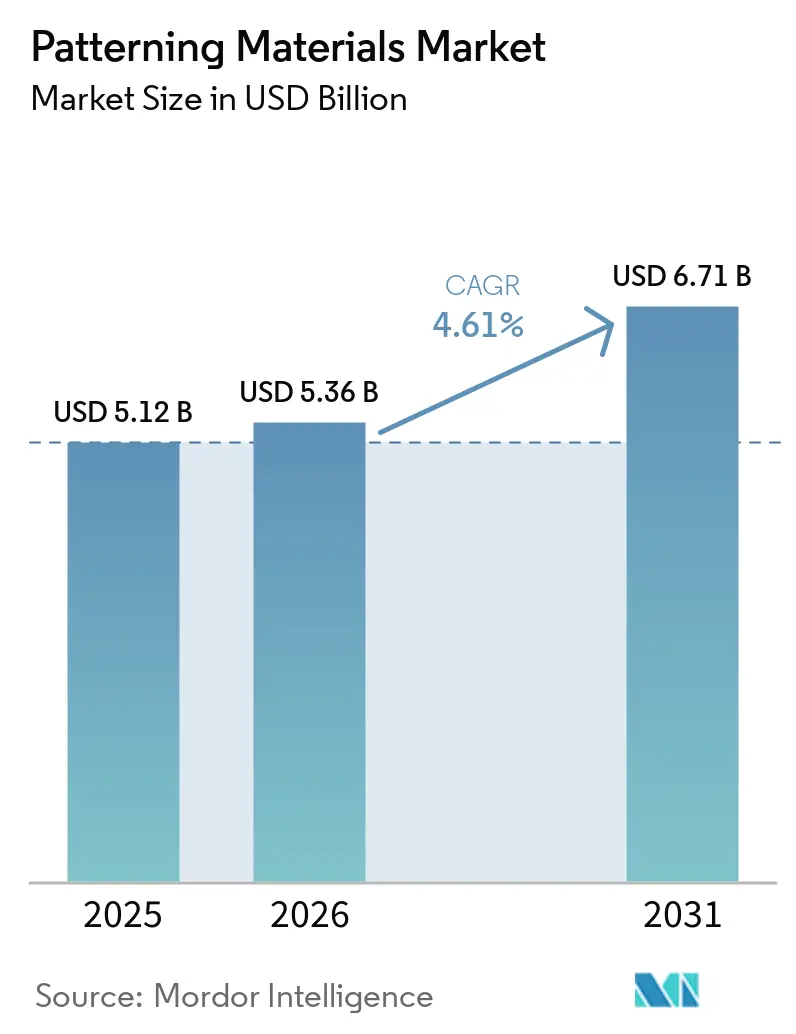
| Market Size (2026) | USD 5.36 Billion |
| Market Size (2031) | USD 6.71 Billion |
| Growth Rate (2026 - 2031) | 4.61% CAGR |
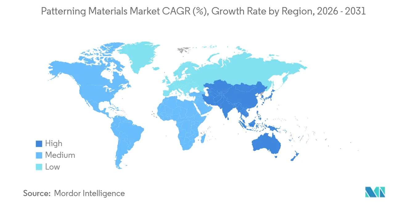
| Fastest Growing Market | Asia Pacific |
| Largest Market | Asia Pacific |
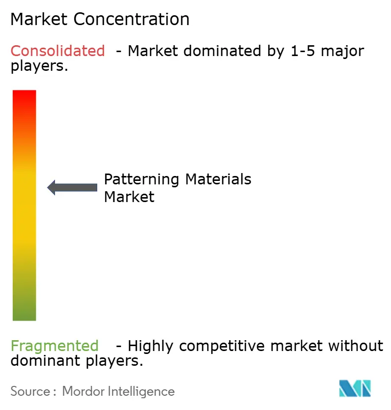
| Market Concentration | Medium |
Major Players *Disclaimer: Major Players sorted in no particular order Image © Mordor Intelligence. Reuse requires attribution under CC BY 4.0. | |
Patterning Materials Market Analysis by Mordor Intelligence
The Patterning Materials Market size is expected to grow from USD 5.12 billion in 2025 to USD 5.36 billion in 2026 and is forecast to reach USD 6.71 billion by 2031 at 4.61% CAGR over 2026-2031. At the sub-3 nm nodes, premium extreme-ultraviolet (EUV) and high-numerical-aperture (high-NA) photoresists are capturing significant value. In contrast, legacy 193 nm dry and immersion chemistries continue to dominate, serving as the high-volume workhorses for mature nodes. These mature nodes primarily cater to sectors such as automotive, industrial, and the Internet of Things. The Asia-Pacific region, bolstered by subsidy-driven expansions in Japan and the establishment of new fabs in China, now accounts for a significant portion of global wafer starts. This dominance ensures a consistent demand for mainstream resists and premium anti-reflective coatings. Geopolitical tensions are reshaping the landscape of patterning materials. Notably, Japan's state-backed acquisition of JSR and its export restrictions have heightened dependency concerns for international buyers. On another front, trends such as automotive electrification, the adoption of back-side power delivery, and the emergence of chiplet packaging are not only modifying resist film thickness requirements but also broadening revenue prospects for specialty formulations. This shift is helping to mitigate unit-price declines in the mature-node segment.
Key Report Takeaways
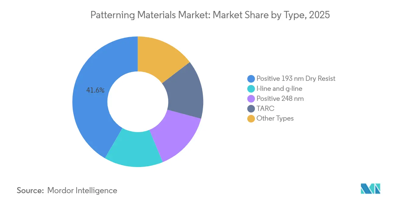
- By type, positive 193 nm dry resist led with 41.62% of the patterning materials market share in 2025. Top anti-reflective coatings are projected to post a 6.54% CAGR to 2031, the fastest among all chemistries.
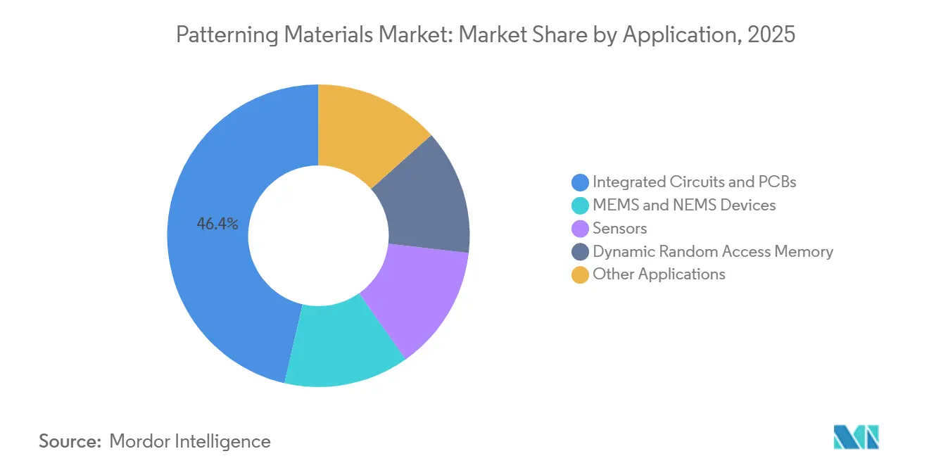
- By application, integrated circuits and PCBs held 46.37% revenue share in 2025, while sensors are forecast to advance at a 7.12% CAGR through 2031.
- By geography, Asia-Pacific accounted for 68.44% of the patterning materials market size in 2025 and is poised for a 6.83% CAGR over 2026-2031.
Note: Market size and forecast figures in this report are generated using Mordor Intelligence’s proprietary estimation framework, updated with the latest available data and insights as of January 2026.
Global Patterning Materials Market Trends and Insights
Drivers Impact Analysis*
| Driver | (~) % Impact on CAGR Forecast | Geographic Relevance | Impact Timeline |
|---|---|---|---|
| Rapid semiconductor fab expansion in Asia-Pacific | +1.80% | China, Japan, South Korea, Taiwan; spill-over to ASEAN | Medium term (2-4 years) |
| EUV and high-NA transition driving advanced resist demand | +1.20% | South Korea, Taiwan, United States | Long term (≥ 4 years) |
| Automotive electronics-led surge in specialty sensors | +0.90% | China, Germany, United States | Medium term (2-4 years) |
| Back-side power delivery and GAA devices altering resist specs | +0.60% | Taiwan, South Korea, United States | Long term (≥ 4 years) |
| On-shoring incentives creating local supply pools | +0.50% | North America, Europe | Medium term (2-4 years) |
| Source: Mordor Intelligence | |||
Rapid Semiconductor Fab Expansion in Asia-Pacific
Between 2026 and 2029, dozens of subsidy-backed fabs, currently under construction in China, Japan, and South Korea, are poised to ramp up monthly production by millions of 300 mm wafer starts. This surge will heighten the structural demand for 193 nm dry, immersion, and top anti-reflective coatings, which are pivotal to the patterning materials market. TSMC has earmarked substantial capital for 2026, with a significant portion aimed at upgrading its Kumamoto campus to 3 nm lines. These advanced lines require both EUV and conventional resists in their multi-layer stacks. In a strategic initiative, Japan’s Ministry of Economy, Trade and Industry has introduced incentives to strengthen local materials manufacturers. This move guarantees a consistent, short-haul supply of high-purity polymers and solvents. On the other hand, China is swiftly establishing 28 nm and 40 nm sites as a countermeasure to export controls. This strategy not only mitigates the impact of these controls but also ensures that positive 193 nm chemistries operate at peak capacity, even as EUV lithography gains traction. The implications of this strategy extend to thick-film resists, which are vital for advanced packaging redistribution layers. This is crucial since every newly designed logic die eventually integrates into a multichip module, demanding a finer RDL pitch.
EUV and High-NA Transition Driving Advanced Resist Demand
By early 2026, ASML’s debut high-NA scanners showcased impressive uptime, efficiently processing a substantial number of wafers[1]ASML Holding NV, “High-NA EUV System Performance,” asml.com . This milestone highlights their commercial viability for nodes at 2 nm and below. The high-NA optics, which reduce the depth of focus by half, require a transition from chemically amplified resists to metal oxide and other high-absorption alternatives. This shift is essential to uphold pattern fidelity in films under 30 nm. ADEKA’s Kashima line, slated to commence in 2028, will supply precursors to industry titans Samsung and SK Hynix. At the same time, Imec has successfully showcased 16 nm pitch capabilities, indicating readiness for mass production. This technology features a shortened exposure time, with metal atoms absorbing significantly more EUV photons. This enhancement not only reduces exposure duration but also lessens the stochastic defect rates typically seen with carbon-based polymers. However, due to capacity constraints, foundries are increasingly securing multi-year supply contracts. While these agreements raise immediate unit costs, they play a crucial role in safeguarding the essential high-NA ramp schedules.
Automotive Electronics-Led Surge in Specialty Sensors
Electric vehicles now house thousands of chips, tripling the count found in traditional internal-combustion models. Most of these chips operate on nodes between 65 nm and 28 nm, leveraging established resist families. Advanced Driver-Assistance Systems (ADAS) demand high-resolution LiDAR, 77 GHz radar, and image sensors. Each component boosts wafer volumes, heightening the demand for thick photoresists designed for high-aspect-ratio MEMS structures. India's Semicon India initiative is enhancing regional capabilities for specialty analog and sensor chips. Concurrently, foundries in Taiwan and South Korea are launching specialty lines tailored for silicon photonics. Moreover, patterned thick films are crucial for creating redistribution layers. These layers seamlessly link sensor dies to compute chiplets in self-driving vehicles, highlighting a cross-industry demand. This expansion broadens the potential market for patterning materials, reaching beyond traditional core logic nodes.
Back-Side Power Delivery and GAA Devices Altering Resist Thickness Specs
Intel’s 18A, TSMC’s upcoming A16, and Samsung’s SF2Z nodes are spearheading a trend by shifting power rails to the wafer's back. This architectural shift demands extra lithography steps on thinned wafers post-bonding, tightening overlay bars to under 5 nm. These back-side contacts necessitate ultra-thin, high-selectivity resists. Such resists must withstand plasma etching while ensuring pristine development on fragile silicon. Simultaneously, the gate-all-around nanosheets are pushing limits, reducing line width roughness budgets to below 2 nm. Lam Research has unveiled a vapor-deposited dry resist prototype, meeting these exacting standards. This prototype offers single-print EUV capabilities at doses under 20 mJ/cm², avoiding the wet processing phase that can distort patterns. Together, these innovations signal a growing revenue stream for metal-organic resists, as the patterning materials market shifts towards cutting-edge sub-1 nm device topologies.
Restraints Impact Analysis*
| Restraint | (~) % Impact on CAGR Forecast | Geographic Relevance | Impact Timeline |
|---|---|---|---|
| High cost and limited capacity of EUV-grade photoresists | -0.80% | South Korea, Taiwan, United States | Short term (≤ 2 years) |
| Stringent solvent-emission regulations | -0.50% | Europe, North America; spill-over to Asia-Pacific | Medium term (2-4 years) |
| Metrology bottlenecks causing defect-related rework | -0.30% | Global; acute at leading-edge fabs | Short term (≤ 2 years) |
| Source: Mordor Intelligence | |||
High Cost and Limited Capacity of EUV-Grade Photoresists
Prices for EUV photoresist are several times higher than those for their 193 nm immersion counterparts. Additionally, EUV photoresists require specialized fluoride-free supply chains, which are rare among industry players. While only ADEKA and Inpria have publicly acknowledged their commercial-scale metal-oxide production, ADEKA's first production line is projected to reach its full capacity only by 2029. Currently, scanner shipments are limited, and orders for each high-NA tool heavily depend on a few long-term supply agreements. In light of this, foundries are overbooking their resist allocations, driving up costs per wafer during initial production ramps. This pricing pressure is underscored by Samsung's 2025 decision to reduce resist dispense per coat, revealing the revenue volatility in the patterning materials market.
Stringent Solvent-Emission Regulations
The European Chemicals Agency (ECHA) is advocating for limits on individual PFAS compounds[2]European Chemicals Agency, “PFAS Restriction Proposal V14,” echa.europa.eu . Such a move could threaten fluoropolymer-rich photoresist topcoats, which might face bans as early as 2028. An analysis by the European Parliament warned that a sweeping ban could lead to substantial losses for the semiconductor sector. As a result, industry lobbyists are pushing for exemptions based on controlled use. Although Fujifilm's fluorine-free ArF Resist and Oji's biomass-based EUV Polymer show technical promise, they consume only a fraction of the liquid volume usually required for spin-coating. This constraint limits supplier revenues and extends the time needed to recoup costs on capital equipment. On top of that, the financial burden of compliance pulls resources away from research and development, hindering innovation in the short term.
*Our forecasts treat driver/restraint impacts as directional, not additive. The impact forecasts reflect baseline growth, mix effects, and variable interactions.
Segment Analysis
By Type: High-Volume 193 nm Platforms Maintain the Revenue Core
In 2025, the market for patterning materials saw a significant contribution from positive 193 nm dry resist, which commanded a 41.62% share. This segment is poised for steady growth, fueled by new Chinese fabs targeting 28 nm and 40 nm lines. On another front, top anti-reflective coatings are projected to grow at a rate of 6.54% during the forecast period of 2026-2031. This growth is largely attributed to the demands of EUV scanners, which require multilayer stacks to reduce reflective notching in high-NA optics. Brewer Science's anti-reflective technology has found a partner in Nissan Chemical. While positive 248 nm resists support legacy logic and thick-film MEMS, their growth is outpaced by the surging demand for newer chemistries. Metal oxide and vapor-deposited dry resists, while leading the pack, face significant uncertainties. Their future hinges on scalable deposition techniques and the regulatory green light for innovative photo-acid generators.
From 2026 to 2031, the competitive landscape is set to heat up. Incumbents in spin-coating are curbing dispense volumes to counter the threat of dry resist disruption. Meanwhile, endorsements from Lam Research and IBM for plasma-developed films, which promise advantages like triple photon absorption and single-print economics, are reshaping the patterning materials market. Once Europe establishes its thresholds, resists devoid of per- and polyfluoroalkyl substances might trigger a similar transformation for 248 nm and i-line materials. Suppliers proficient in both metal-oxide and fluorine-free polymers are poised to capture additional revenue streams by 2030.


By Application: Sensors Accelerate, IC Revenue Holds Dominance
In 2025, integrated circuits and PCBs accounted for 46.37% of the revenue, driven by logic and memory devices. These devices managed to stabilize average selling prices, countering a slowdown in wafer-start growth. As dynamic random-access memory (DRAM) increasingly adopts EUV lithography, Samsung's introduction of HBM4 raises the stakes for ultra-thin wafer resists in 16-layer 3D stacks. The patterning materials market for the IC segment is on a steady growth trajectory during the forecast period of 2026-2031. However, sensors are outpacing all other applications, boasting a 7.12% CAGR. This surge is fueled by the growing integration of radar, LiDAR, and high-resolution imaging in advanced driver-assistance systems. As thick-film chemistries find applications in MEMS mirrors and pressure diaphragms, niche suppliers are discovering avenues beyond the saturated logic market.
Geographic diversification is on the rise: India is championing mature-node fabs for sensors and analog outputs, while ASEAN nations are bolstering assembly plants for redistribution layers. There is a notable uptick in demand for chemically amplified resists, particularly for patterned RDL lines under 2 µm. These are being tailored for wafer-level fan-out, in line with the burgeoning trend of chiplet architecture. The emergence of multi-application modules means that every camera or radar board now mandates at least two lithography passes at the package level. This requirement not only amplifies the total resist volume per IC but also highlights the diversification within the patterning materials market.
Geography Analysis
Asia-Pacific, accounting for 68.44% of global consumption in 2025, is projected to grow at a 6.83% CAGR through 2031. This growth is largely fueled by subsidy pools in Japan, China, and South Korea, bolstering their foundry and material ecosystems. In this region, JSR, Tokyo Ohka Kogyo, and Shin-Etsu Chemical dominate, leading the export of merchant photoresists. These companies strategically wield export licenses, enabling them to influence global wafer-start plans within weeks. While China's new fabs are set to outpace Taiwan in mature-node output by 2027, they still heavily depend on high-purity resist imports from Japan. This reliance makes China's national champions vulnerable to disruptions, especially given the current geopolitical climate.
North America, buoyed by the CHIPS Act, is witnessing a flurry of activity: Intel's mega-site in Ohio, TSMC's campus in Arizona, and Samsung's project in Taylor are all gearing up for substantial monthly wafer starts by 2030. DuPont is aggressively expanding, doubling its resist capacity at the Sasakami plant and debuting an advanced pilot line in Texas. Lam Research is making waves, introducing its Aether dry resist to U.S. logic producers. Despite facing approval backlogs for new photo-acid generators, multi-agency task forces, with defense funding backing, are hastening reviews, underscoring the region's commitment to the patterning materials market.
Europe, the smallest of the three core demand zones, is witnessing a surge in legislative activity. ESMC's Dresden fab, under the aegis of the EU Chips Act 2.0, is locally producing nodes for automotive applications. This has prompted Merck and BASF to boost their regional high-purity solvent output. However, ongoing discussions around PFAS cast a shadow on long-term prospects; a stringent threshold might necessitate a complete reformulation of every resist family. Suppliers are preemptively co-locating research and development in Japanese cleanrooms, where PFAS restrictions are more lenient. This move, while safeguarding their interests, inadvertently shifts intellectual property away from Europe, even as the wafer starts expanding within the continent.

Competitive Landscape
The patterning materials market is moderately consolidated. Three Japanese giants - JSR, Tokyo Ohka Kogyo, and Shin-Etsu Chemical - dominate the merchant photoresist landscape. Concurrently, four upstream vendors of resin and photo-acid generators command a significant share of the specialty monomer market. In a strategic move, Japan's state-backed acquisition of JSR in 2025 not only secures national control but also facilitates selective export curbs, a tactic already employed to halt shipments to China in late 2025. South Korea, through initiatives like SK Hynix and Dongjin Semichem's EUV program, is ambitiously targeting a reduction in import dependence by 2030. However, achieving full substitution remains a challenge, especially with qualification hurdles at the 2 nm nodes.
Disruption is anticipated in the realms of metal-oxide resists and fluorine-free polymers. ADEKA's Kashima plant is set to unveil the first high-volume metal-oxide line in 2028. Yet, with limited capacity, scarcity looms for at least the subsequent three years. Lam Research is betting on its vapor-deposited dry resist, positioning it as a process-integrated alternative. By bundling etch tools and deposition chambers into turnkey modules, they aim to capture a significant market share of advanced-node coatings by 2031, contingent on adoption rates. Incumbents are diversifying through strategic alliances: TSMC is channeling resources into joint research and development with Shin-Etsu and JSR, aiming to pioneer 2 nm resists. Simultaneously, Tokyo Ohka Kogyo is investing in a South Korean facility, a move to appease local clientele amidst export tensions.
Regulatory landscapes are intensifying the competitive race. Fujifilm's fluorine-free ArF and nanoimprint offerings have secured early environmental nods, providing fabs with compliance assurance, albeit at a slight performance trade-off. Oji's biomass EUV resist, showcasing sensitivity boosts in lab evaluations, still faces the hurdle of passing comprehensive stochastic variability assessments. The Ministry of Economy, Trade and Industry is spearheading an open development hub for high-NA EUV in Hokkaido, slated for 2029. This initiative, pooling national expertise, holds the potential to set global standards, further cementing Japan's stature as a pivotal technology gatekeeper in the patterning materials arena.
Patterning Materials Industry Leaders
DuPont
Fujifilm Holdings Corporation
JSR Corporation
Shin-Etsu Chemical Co., Ltd
- *Disclaimer: Major Players sorted in no particular order

Recent Industry Developments
- March 2026: Lam Research and IBM Research began a five-year collaboration at Albany NanoTech Complex to integrate Aether vapor-deposited dry resist with high-NA EUV process flows, targeting sub-1 nm nodes
- March 2026: JK Materials Co., one of the leading providers of specialty semiconductor materials, has completed the construction of a new manufacturing facility. This plant is set to produce a comprehensive range of semiconductor patterning materials.


Global Patterning Materials Market Report Scope
Patterning is a photolithography technique essential for creating integrated circuits on wafers during the electronic device fabrication process. Patterning materials refer to polymer films, also known as photoresists, which are patterned by exposing them to light of specific wavelengths. These materials are primarily used in the manufacturing of printed circuit boards.
The Patterning Materials Market is segmented by type, application, and geography. By type, the market is segmented into I-line and G-line, positive 248 nm, positive 193 nm dry resist, TARC, and other types. By application, the market is segmented into integrated circuits and PCBs, MEMS and NEMS devices, sensors, dynamic random access memory, and other applications. The report also covers the market size and forecasts for patterning materials in 11 countries across major regions. For each segment, the market sizing and forecasts have been done on the basis of value (USD).
| I-line and g-line |
| Positive 248 nm |
| Positive 193 nm Dry Resist |
| TARC |
| Other Types |
| Integrated Circuits and PCBs |
| MEMS and NEMS Devices |
| Sensors |
| Dynamic Random Access Memory |
| Other Applications |
| Asia-Pacific | China |
| India | |
| Japan | |
| South Korea | |
| ASEAN Countries | |
| Rest of Asia-Pacific | |
| North America | United States |
| Canada | |
| Mexico | |
| Europe | Germany |
| United Kingdom | |
| France | |
| Italy | |
| Rest of Europe | |
| Rest of the World |
| By Type | I-line and g-line | |
| Positive 248 nm | ||
| Positive 193 nm Dry Resist | ||
| TARC | ||
| Other Types | ||
| By Application | Integrated Circuits and PCBs | |
| MEMS and NEMS Devices | ||
| Sensors | ||
| Dynamic Random Access Memory | ||
| Other Applications | ||
| By Geography | Asia-Pacific | China |
| India | ||
| Japan | ||
| South Korea | ||
| ASEAN Countries | ||
| Rest of Asia-Pacific | ||
| North America | United States | |
| Canada | ||
| Mexico | ||
| Europe | Germany | |
| United Kingdom | ||
| France | ||
| Italy | ||
| Rest of Europe | ||
| Rest of the World | ||


Key Questions Answered in the Report
What is the projected value of the patterning materials market in 2031?
The patterning materials market size stands at USD 5.36 billion in 2026, and it is projected to reach USD 6.71 billion by 2031 at a 4.61% CAGR.
Which resist chemistry currently holds the largest share?
Positive 193 nm dry resist accounted for 41.62% of global revenue in 2025.
Which application segment will grow the fastest through 2031?
Sensors are forecast to post a 7.12% CAGR, outpacing all other end-uses.
Why are metal-oxide resists important for next-generation lithography?
They absorb 3-5 times more EUV photons than carbon-based polymers, enabling single-print patterning at sub-2 nm nodes.
How will PFAS regulation influence suppliers?
Stricter limits may force rapid transition to fluorine-free resists, compelling suppliers to overhaul product lines or risk market access.
Page last updated on:


