
Technology, Media and Telecom
5th MayPricing Strategy for Semiconductor Components
3 Min Read
North America Atomic Layer Deposition Market Segmented by Application (Semiconductor & Electronics, Healthcare & Biomedical, and More), Deposition Method (Thermal ALD, Plasma-Enhanced ALD and More), Equipment Type (Batch Reactors, Single-Wafer Reactors and More), Precursor Chemistry (Metal Oxides, Metal Nitrides, and More), and Geography. The Market Forecasts are Provided in Terms of Value (USD).
Market Overview
| Study Period | 2019 - 2030 |
|---|---|
| Base Year For Estimation | 2024 |
| Forecast Data Period | 2025 - 2030 |
| Market Size (2025) | USD 0.74 Billion |
| Market Size (2030) | USD 1.23 Billion |
| Growth Rate (2025 - 2030) | 10.64 % CAGR |
| Market Concentration | High |
Major Players *Disclaimer: Major Players sorted in no particular order. Image © Mordor Intelligence. Reuse requires attribution under CC BY 4.0. |
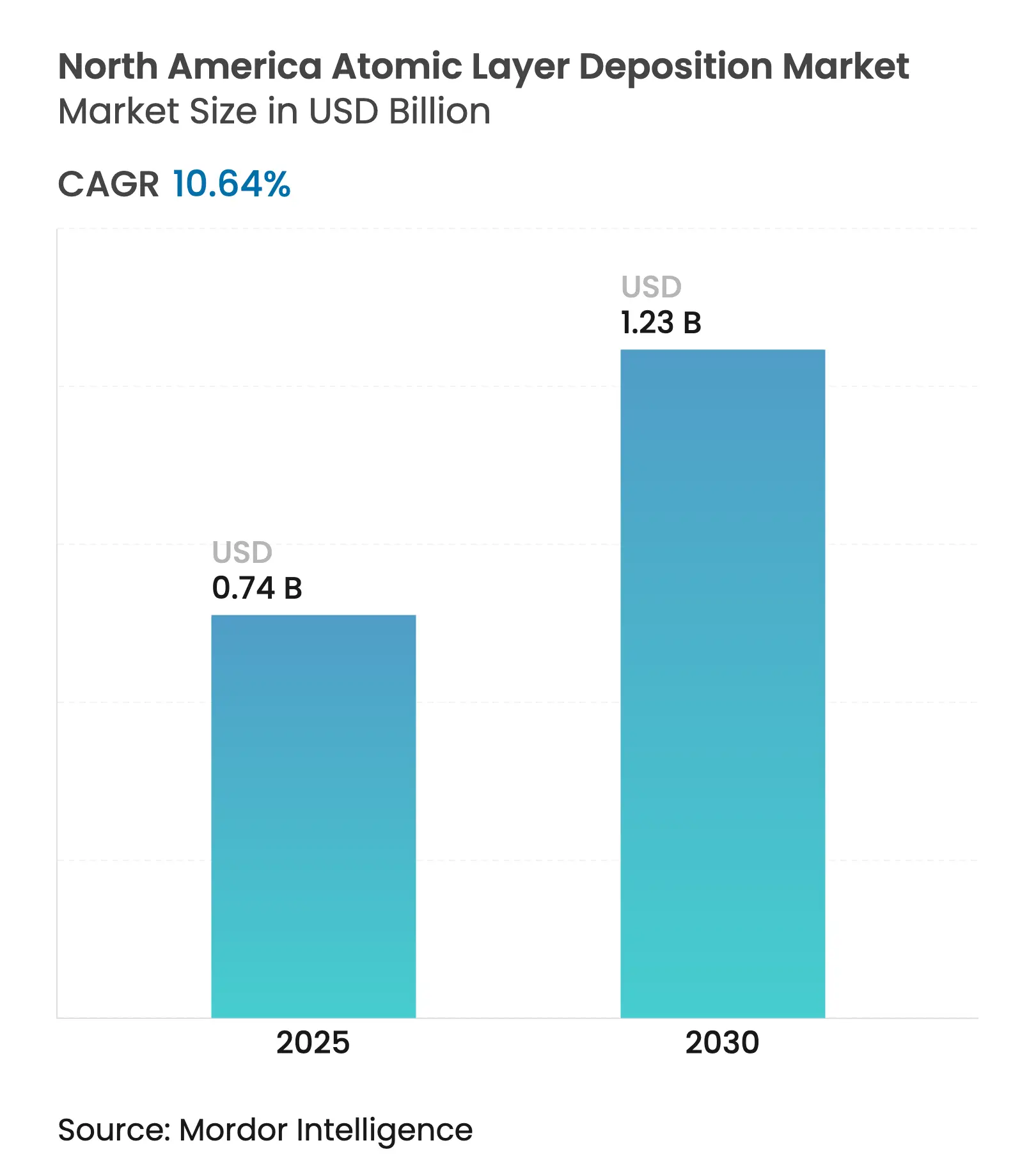
The North America atomic layer deposition market reached USD 0.74 billion in 2025 and is forecast to attain USD 1.23 billion by 2030, rising at a 10.64% CAGR. This growth rests on the region’s position as a front-line semiconductor manufacturing hub, with state incentives, expanding fab footprints and rising demand for atomic-scale precision across batteries, photovoltaics and flexible electronics. Major foundries are shifting sub-3 nm logic and 3D-NAND memory to high-volume runs, pulling in new ALD tool orders even before clean-room construction is complete. The United States captures the bulk of regional revenue thanks to the USD 52 billion CHIPS Act, while Mexico’s near-shoring wave fuels the fastest growth. Thermal ALD retains process leadership, yet spatial ALD and roll-to-roll systems attract outsized capital as producers weigh throughput gains against higher capex. Supply chain gaps around ultra-high-purity valves and precursor chemistry linger, but joint ventures between tool makers, gas suppliers and chemical companies aim to localize critical inputs.[1]Applied Materials, “Applied Materials Reports Second Quarter 2025 Results,” appliedmaterials.com
Key Report Takeaways
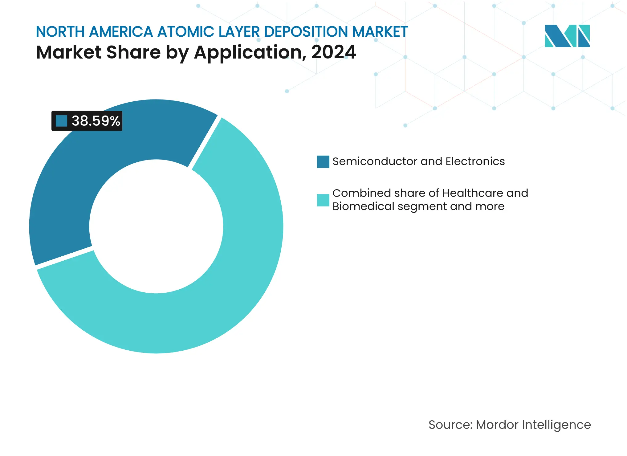
By application, semiconductor and electronics led with 38.59% revenue share in 2024; energy and solar is projected to expand at a 13.99% CAGR to 2030.
By deposition method, thermal ALD held 40.23% of the North America atomic layer deposition market share in 2024, while spatial ALD is on track for 15.40% CAGR through 2030.
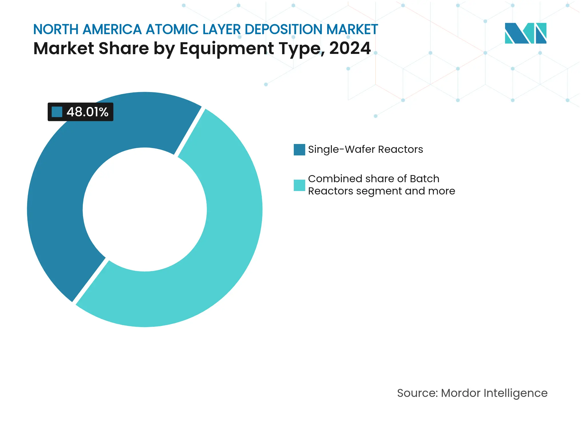
By equipment type, single-wafer reactors accounted for 48.01% share of the North America atomic layer deposition market size in 2024; roll-to-roll tools are advancing at a 14.20% CAGR between 2025-2030.
By precursor chemistry, metal oxides captured 65.10% share in 2024; metal nitrides are positioned for 16.72% CAGR to 2030.
By geography, the United States commanded 84.60% share of regional revenue in 2024; Mexico posts the strongest 2025-2030 CAGR at 15.51%.
ASM International and Tokyo Electron jointly controlled 48% of the North America atomic layer deposition market share in 2024.
Drivers Impact Analysis
| Driver | (~) % Impact on CAGR Forecast | Geographic Relevance | Impact Timeline | |||
|---|---|---|---|---|---|---|
Semiconductor capacity race drives ALD tool installs Semiconductor capacity race drives ALD tool installs | 2.50% | United States, with spillover to Mexico | Medium term (2-4 years) | (~) % Impact on CAGR Forecast:2.50% | Geographic Relevance:United States, with spillover to Mexico | Impact Timeline:Medium term (2-4 years) |
U.S. CHIPS Act cap-ex incentives accelerate fab spend U.S. CHIPS Act cap-ex incentives accelerate fab spend | 1.80% | United States primarily, indirect benefits to Canada | Short term (≤ 2 years) | |||
Rise of 3D-NAND & GAA transistors increases ALD steps Rise of 3D-NAND & GAA transistors increases ALD steps | 2.10% | North America, concentrated in advanced fab locations | Long term (≥ 4 years) | |||
Accelerated R&D in solid-state batteries (protective films) Accelerated R&D in solid-state batteries (protective films) | 1.60% | United States and Canada, emerging in Mexico | Medium term (2-4 years) | |||
Under-reported: Roll-to-roll ALD lines for flexible sensors Under-reported: Roll-to-roll ALD lines for flexible sensors | 0.90% | United States, with pilot programs in Canada | Long term (≥ 4 years) | |||
Under-reported: Low-temp PEALD for packaging barrier films Under-reported: Low-temp PEALD for packaging barrier films | 0.50% | North America, driven by consumer electronics demand | Medium term (2-4 years) | |||
| Source: Mordor Intelligence | ||||||
Semiconductor capacity race drives ALD tool installs
Foundries racing toward sub-3 nm nodes are locking in multi-year supply agreements for high-throughput reactors, lifting order backlogs for Applied Materials and Lam Research. Tokyo Electron has committed JPY 1.5 trillion to expand process-equipment RandD, with significant allocations to ALD platforms. Device complexity, multilayer gate stacks and 200-plus deposition cycles for 3D-NAND push ALD tool time to more than 40% of total wafer hours, embedding the technology deeper into fab process flows.[2]Entegris, “Entegris Announces Expansion to Support Semiconductor Materials,” entegris.com
U.S. CHIPS Act cap-ex incentives accelerate fab spend
Federal grants and tax credits pull forward build-outs in Arizona, Ohio and Idaho, where Intel, Micron and TSMC are adding capacity that mandates new ALD chambers for logic, memory and advanced packaging. Entegris expanded a USD 75 million facility to supply ultra-high-purity materials, while Air Liquide committed over USD 250 million for high-purity gas plants linked to Micron’s memory project. The incentive window compresses typical procurement cycles, prompting equipment reservations years ahead of tool move-in milestones.
Rise of 3D-NAND and GAA transistors increases ALD steps
Transitioning from FinFET to gate-all-around structures multiplies conformal dielectric and metal layers per device, with some GAA flows exceeding 50 individual ALD cycles. In 3D-NAND, >200 active layers each demand angstrom-level uniformity, driving wafer-per-year forecasts for ALD equipment to new highs. The requirement for perfect step coverage on deep, high-aspect features cements ALD as irreplaceable in future nodes.
Accelerated RandD in solid-state batteries (protective films)
Argonne National Laboratory demonstrated ALD-deposited lithium phosphorus oxynitride films that improve cycle life and thermal stability in solid-state cells. Automakers target commercial launches by 2028, prompting equipment makers to customize reactors for battery-scale substrates. Altech’s EUR 684 million coating facility illustrates commercial momentum, citing 30% energy-retention gains from ALD layers.[4]Argonne National Laboratory, “ALD-Developed Protective Layers Advance Solid-State Batteries,” anl.gov
Restraints Impact Analysis
| Restraint | (~) % Impact on CAGR Forecast | Geographic Relevance | Impact Timeline | |||
|---|---|---|---|---|---|---|
High cost of halide & metal-organic precursors High cost of halide & metal-organic precursors | -1.80% | North America, with acute impact in Canada and Mexico | Short term (≤ 2 years) | (~) % Impact on CAGR Forecast:-1.80% | Geographic Relevance:North America, with acute impact in Canada and Mexico | Impact Timeline:Short term (≤ 2 years) |
Tool throughput limits vs. CVD/Sputter alternatives Tool throughput limits vs. CVD/Sputter alternatives | -1.20% | United States primarily, affecting high-volume applications | Medium term (2-4 years) | |||
Under-reported: Scarcity of UHP valve/liner supply chain Under-reported: Scarcity of UHP valve/liner supply chain | -0.90% | North America, concentrated in advanced fab locations | Short term (≤ 2 years) | |||
Under-reported: Tight patent pool blocking start-ups Under-reported: Tight patent pool blocking start-ups | -0.60% | United States, with spillover effects to innovation hubs | Long term (≥ 4 years) | |||
| Source: Mordor Intelligence | ||||||
High cost of halide and metal-organic precursors
Advanced precursors often exceed USD 10,000 per kilogram, squeezing margins for cost-sensitive photovoltaic and flexible-electronics producers. Limited qualified suppliers strengthen pricing power; Air Liquide’s new Idaho plant seeks to localize capacity and moderate price swings. Recycling and alternative chemistries are under exploration, yet broad commercial roll-out remains several years away.
Tool throughput limits vs. CVD/Sputter alternatives
Classic thermal ALD struggles to top 20 wafers per hour, versus 100+ for CVD. Spatial ALD now delivers 3-5× higher rates, but capex premiums delay adoption outside leading-edge fabs. Roll-to-roll lines show promise for foils and polymers, though recipe transfer from vacuum batch systems requires extensive re-qualification.
By Application: Semiconductor leadership anchors expansion
The semiconductor and electronics segment secured 38.59% of 2024 revenue, underscoring ALD’s indispensable role in logic scaling, memory stacking and advanced packaging within the North America atomic layer deposition market. Capital inflows from AI accelerators and edge devices magnify layer counts, locking in tool demand grounded in strict defectivity limits. Energy and solar post the fastest projected 13.99% CAGR, lifted by solid-state battery commercialization timelines and next-generation tandem PV designs that need pinhole-free passivation.
Healthcare coatings, implantable devices and diagnostic optics add complementary growth paths. Automotive power electronics gain from ALD-derived high-k dielectrics that suppress leakage currents. These cross-industry pull factors diversify revenue and insulate the North America atomic layer deposition market from single-sector downturns.
Note: Segment shares of all individual segments available upon report purchase
By Deposition Method: Thermal ALD keeps process share
Thermal activation retained 40.23% of 2024 spending by delivering proven conformality and broad materials libraries, preserving its seat in every leading-edge fab recipe. Nonetheless, spatial ALD’s 15.40% forecast CAGR highlights a throughput-driven pivot, especially where panel-scale or polymer substrates dominate. Plasma-enhanced ALD fills the low-temperature niche for OLEDs and advanced packaging, while roll-to-roll pilots address volume economics for flexible barriers.
Higher productivity variants shift cost curves, yet incremental learning cycles and spare-parts ecosystems favor entrenched thermal platforms for the near term. As spatial reactors mature, producers anticipate hybrid lines that merge spatial pre-fill and thermal finish steps to balance rate, uniformity and particle performance.
By Equipment Type: Single-wafer reactors dominate installations
Single-wafer tools represented 48.01% of installed base in 2024 because fabs prize tight thickness control, chamber-to-chamber tuning and recipe flexibility across multiple device nodes. Their prevalence reinforces service-network density and second-hand market liquidity, anchoring vendor lock-in within the North America atomic layer deposition market size.
Batch reactors retain momentum in back-end processes and cost-centric analog lines. Roll-to-roll systems, growing at 14.20% CAGR, appeal to flexible electronics and moisture-barrier packaging, where substrate form factors demand continuous transport. Modular pilot tools facilitate recipe proof-of-concept, mitigating risk before full capital commitments.
Note: Segment shares of all individual segments available upon report purchase
By Precursor Chemistry: Metal oxides set the baseline
Metal oxides delivered 65.10% revenue in 2024, led by Al₂O₃, HfO₂ and ZrO₂ layers etched into every advanced transistor and DRAM capacitor. Their mature supply chain and well-mapped process windows keep cost profiles predictable. Metal nitrides rise at 16.72% CAGR through 2030, propelled by work-function tuning in GAA gates and diffusion barriers in copper-interconnect replacements.
Sulfides and fluorides support memory select layers and extreme-optic coatings. Hybrid organic and ternary systems gain mindshare as area-selective ALD enables molecule-level patterning, an emerging differentiator for next-decade logic nodes.
The United States held 84.60% of 2024 spending, underpinned by multi-billion-dollar fab expansions, robust RandD infrastructure and a dense ecosystem of tool, gas and precursor suppliers. Federal incentives accelerate time-to-ramp and enhance service-logistics footprints that anchor the North America atomic layer deposition market. State-level grants in Arizona, Ohio and Texas complement federal funding and foster a self-reinforcing cluster of skills, suppliers and pilot lines.
Canada contributes niche growth through aerospace coatings, quantum-computing devices and government-funded battery pilots. Partnerships between universities and small tool builders nurture novel PEALD recipes targeting low-temperature substrates. Provincial clean-energy mandates further lift demand for ALD-enabled PV passivation.
Mexico registers the highest 15.51% CAGR as EMS firms and automotive Tier 1s bring packaging, sensor and power-module assembly closer to final vehicle lines. Incentives within industrial parks near the U.S. border, coupled with skill-development programs, shorten supply chains and spread ALD know-how across the broader North America atomic layer deposition market.
Market Concentration
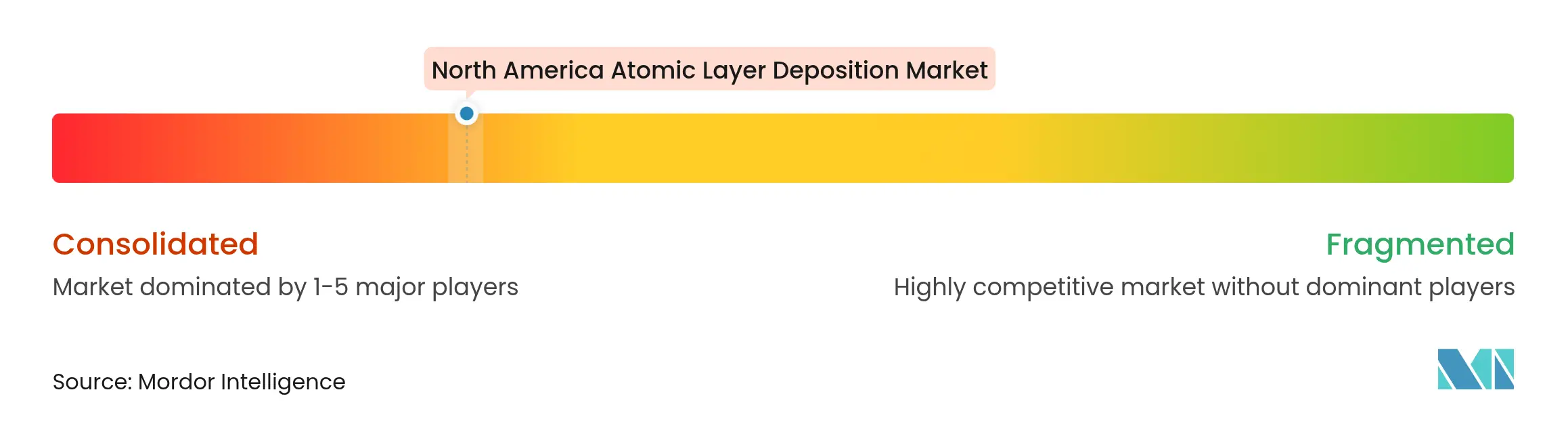
Market concentration is moderate. ASM International led with roughly 30% share in 2024, benefiting from deep IP portfolios and early engagement in GAA tool co-development. Tokyo Electron followed at 18%, leveraging cross-platform synergies with etch and clean equipment. Applied Materials and Lam Research compete for advanced memory slots, each citing record ALD revenue in recent filings.
Emerging specialists such as Forge Nano target particle-coating systems for battery powders, while Picosun USA advances compact cluster tools for pilot fabs. Patent thickets around valve geometry, precursor trapping and in-situ metrology constrain new entrants, steering many toward niche chemistries or flexible substrates.
Service models shift from transaction to outcome-based contracts. Vendors bundle AI-driven recipe optimization and predictive maintenance to secure multi-year deals. Partnerships between tool makers and gas suppliers co-locate spare-part depots near new fabs, reducing mean-time-to-repair and improving uptime metrics critical to the expanding North America atomic layer deposition industry.[3]Phys.org, “Machine Learning Accelerates ALD Precursor Design,” phys.org

*Disclaimer: Major Players sorted in no particular order
1. INTRODUCTION
2. RESEARCH METHODOLOGY
3. EXECUTIVE SUMMARY
4. MARKET LANDSCAPE
5. MARKET SIZE and GROWTH FORECASTS
6. COMPETITIVE LANDSCAPE
7. MARKET OPPORTUNITIES and FUTURE OUTLOOK
The report on the North American atomic layer deposition market is limited to the semiconductor and electronics, healthcare and biomedical, automotive, and other applications in the United States and Canada.
Pricing Strategy for Semiconductor Components
3 Min Read
Accelerating Additive Manufacturing Adoption in India
3 Min Read
When decisions matter, industry leaders turn to our analysts. Let’s talk.