
Lensless Industrial Imaging Market Size and Share
Market Overview
| Study Period | 2020 - 2031 |
|---|---|
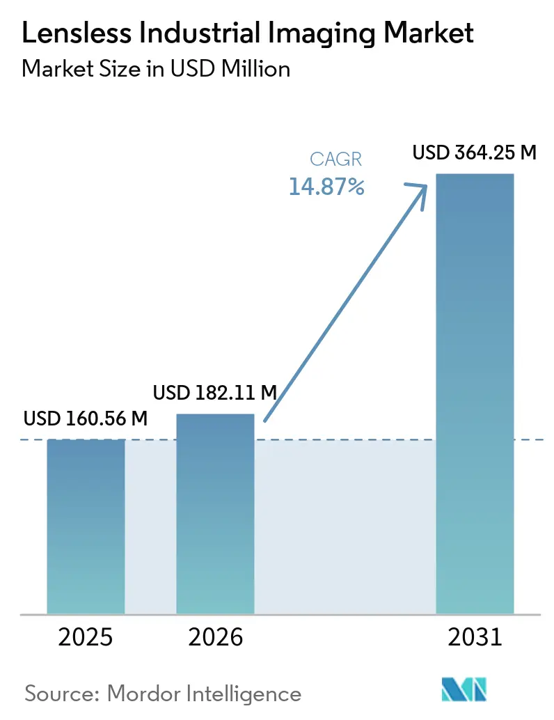
| Market Size (2026) | USD 182.11 Million |
| Market Size (2031) | USD 364.25 Million |
| Growth Rate (2026 - 2031) | 14.87 % |
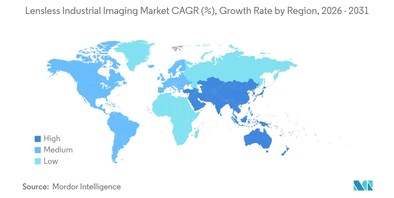
| Fastest Growing Market | Asia-Pacific |
| Largest Market | Asia-Pacific |
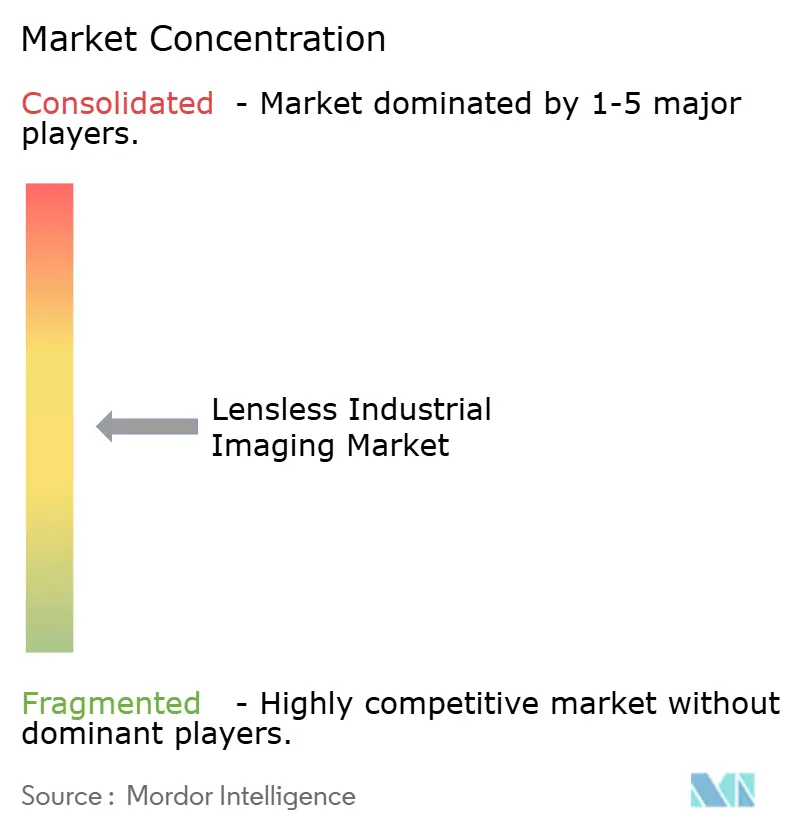
| Market Concentration | Medium |
Major Players *Disclaimer: Major Players sorted in no particular order Image © Mordor Intelligence. Reuse requires attribution under CC BY 4.0. | |
Lensless Industrial Imaging Market Analysis by Mordor Intelligence
The lensless industrial imaging market size is projected to expand from USD 160.56 million in 2025 and USD 182.11 million in 2026 to USD 364.25 million by 2031, registering a CAGR of 14.87% between 2026 and 2031. Software that reconstructs usable images from encoded light patterns is becoming more practical for factory environments. Advanced semiconductor packaging needs inspection methods that can operate in confined spaces and capture phase information. Robotics designers also need thin sensors that fit within grippers, joints, and other tight spaces. These conditions move the Lensless industrial imaging market beyond laboratory use and into manufacturing qualification programs. Adoption will still depend on computing capacity, validation data, and integration with established machine-vision workflows.
Key Report Takeaways
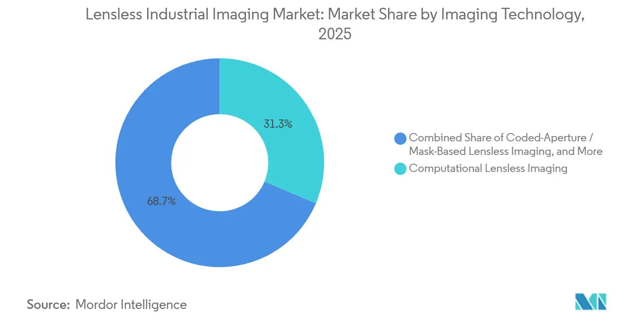
- By imaging technology, computational lensless imaging held 31.34% of the Lensless industrial imaging market share in 2025, while metasurface and metalens-enabled lensless imaging is projected to expand at a 15.67% CAGR through 2031.
- By application, machine vision and quality inspection held 27.78% of the Lensless industrial imaging market share in 2025, while robotics and automated systems is projected to expand at a 15.54% CAGR through 2031.
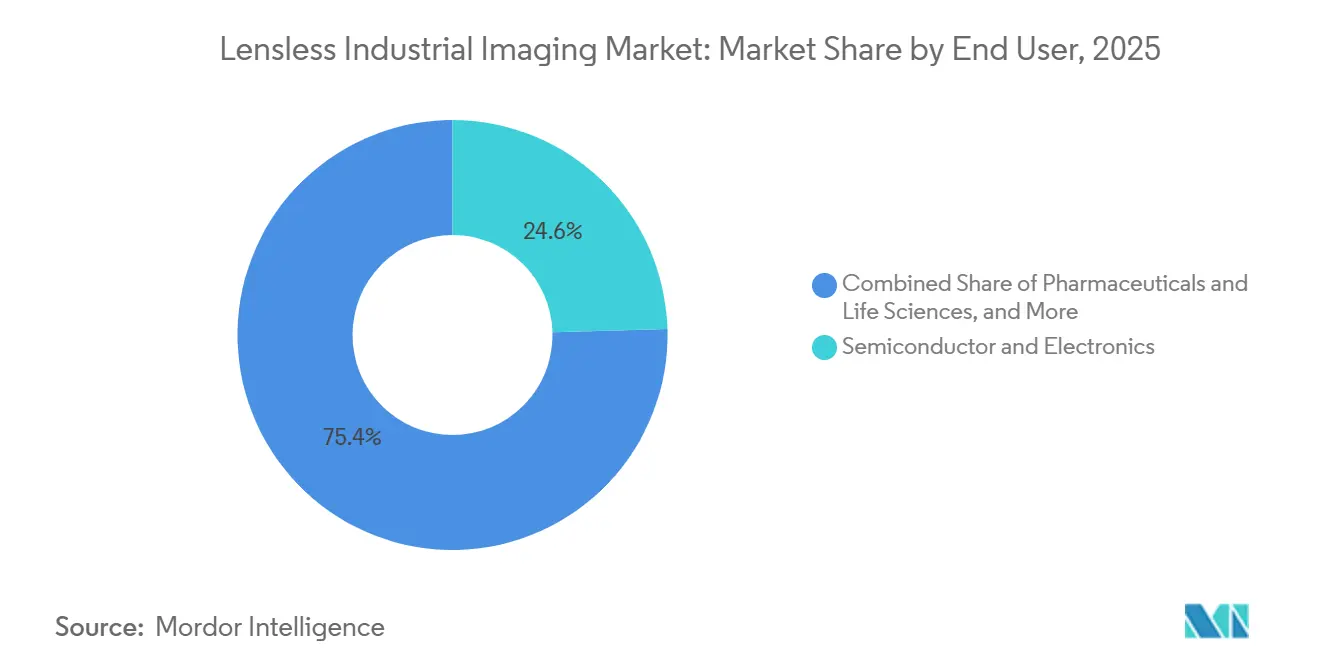
- By end user, semiconductor and electronics held 24.56% of the Lensless industrial imaging market share in 2025 and is projected to expand at a 15.89% CAGR through 2031.
- By form factor, inline machine-mounted systems held 27.72% of revenue in 2025, while sub-millimeter embedded modules are projected to expand at a 15.41% CAGR through 2031.
- By geography, Asia-Pacific held 36.42% of revenue in 2025 and is projected to expand at a 15.32% CAGR through 2031.
Key Report Takeaways
| Segmentation | Segment | Metric | Year | Value |
|---|---|---|---|---|
| By Imaging Technology | Computational Lensless Imaging | Market Share | 2025 | 31.34% |
| By Imaging Technology | Metasurface and Metalens-Enabled Lensless Imaging | CAGR | 2031 | 15.67% |
| By Application | Machine Vision and Quality Inspection | Market Share | 2025 | 27.78% |
| By Application | Robotics and Automated Systems | CAGR | 2031 | 15.54% |
| By End User | Semiconductor and Electronics | Market Share | 2025 | 24.56% |
| By End User | Semiconductor and Electronics | CAGR | 2031 | 15.89% |
| By Form Factor | Inline Machine-Mounted Systems | Market Share | 2025 | 27.72% |
| By Form Factor | Sub-Millimeter Embedded Modules | CAGR | 2031 | 15.41% |
| By Geography | Asia-Pacific | Market Share | 2025 | 36.42% |
| By Geography | Asia-Pacific | CAGR | 2031 | 15.32% |
| Source: Mordor Intelligence | ||||
Note: Market size and forecast figures in this report are generated using Mordor Intelligence’s proprietary estimation framework, updated with the latest available data and insights as of January 2026.
Global Lensless Industrial Imaging Market Trends and Insights
Drivers Impact Analysis*
| Driver | (~) % Impact on CAGR Forecast | Geographic Relevance | Impact Timeline |
|---|---|---|---|
| AI-Assisted Image Reconstruction and Defect Classification | +3.0% | Global, concentrated in North America and East Asia | Short term (≤ 2 years) |
| Semiconductor and Advanced Display Inspection Complexity | +1.8% | Asia-Pacific core, with spillover to North America | Medium term (2-4 years) |
| Demand for Ultra-Compact Imaging at Robotic End Effectors | +1.4% | Global, with strength in Germany, Japan, China, and the United States | Short term (≤ 2 years) |
| Growth of Inline, Non-Contact Metrology | +0.8% | North America and Europe, expanding to Asia-Pacific | Medium term (2-4 years) |
| Confidentiality Benefits of Encoded Sensor Outputs | +0.2% | Aerospace and defense corridors in North America and Europe | Long term (≥ 4 years) |
| Reduced Calibration and Maintenance from Passive Optics | +0.1% | Global | Medium term (2-4 years) |
| Source: Mordor Intelligence | |||
AI-Assisted Image Reconstruction and Defect Classification
The Lensless industrial imaging market depends on software that converts a diffraction pattern into a usable image and defect map. Physics-guided neural networks combine a physical forward model with learned reconstruction steps to improve results under model uncertainty. Reflective through-silicon phase imaging resolved 2.19-µm features using a lensless approach, which supports inspection where mechanically driven focusing adds alignment risk.[1] Self-supervised methods can train without paired reference images from lensed cameras, reducing dependence on calibration setups that may introduce bias. These methods can make reconstruction more suitable for embedded industrial controllers. Cognex introduced an embedded AI vision system powered by Qualcomm Dragonwing in May 2026, showing that industrial vision platforms are adding more local processing capacity. Physics-guided reconstruction also helps systems separate meaningful process variation from optical artifacts without adding moving optical assemblies. This can reduce alignment-related interruptions in high-throughput packaging cells where each inspection stage must fit into a tightly controlled process flow.
Semiconductor and Advanced Display Inspection Complexity
The Lensless industrial imaging market benefits from tighter dimensions in semiconductor and display manufacturing. Gate-all-around nodes below 2 nm and hybrid-bonding pitches below 10 µm increase the difficulty of achieving resolution, working distance, and throughput in one inspection step. Reflective lensless phase imaging can create micrometer-scale alignment maps from a single diffraction capture for die-to-wafer stacking. This removes a mechanical focus step that can limit bonding-tool throughput. Hamamatsu began accepting orders for a ThermoDynamic imaging module for its PHEMOS-X series in May 2025, focused on generative AI chip structures with small, three-dimensional geometries. Equipment choices will also need to meet semiconductor safety and operating requirements, including the standards used by fabrication facilities. Coherent diffraction methods are relevant because they can recover information from complex surfaces and confined interfaces without the mechanical arrangement required by objective lenses. Semiconductor suppliers in Japan and South Korea are therefore important early users, while safety and equipment requirements continue to influence how these systems are configured.
Demand for Ultra-Compact Imaging at Robotic End Effectors
The Lensless industrial imaging market is gaining support from robotic applications where conventional camera housings cannot fit. Collaborative robots and humanoid platforms require sensors for fingertip, joint-pocket, and suction-cup locations. ThinTact, a lensless tactile sensor, demonstrated a 200-mm² sensing field in a structure under 10 mm thick.[2] The study used a discrete cosine transform-based method for real-time reconstruction, showing how sensor geometry and processing design must work together. Such modules can be specified during robot design rather than installed later by integrators. That shift can increase unit volumes while placing pressure on component pricing and qualification cycles. Event-based sensing can further reduce the data transferred to robot controllers by recording pixel-level changes rather than complete frames during idle movement. This makes lensless architectures more relevant for robotic systems that must balance compact hardware, power limits, and prompt control responses.
Growth of Inline, Non-Contact Metrology
The Lensless industrial imaging market is also supported by the move from laboratory measurement to permanent inline inspection. Lensless systems can reduce the need for objective lenses, autofocus actuators, and mechanical scanning stages. A metalens-based Fizeau interferometer reported a 6.5 × 10 × 5 mm package and 44-nm step-height measurement fidelity.[3] A separate computational metrology method reported nanometer-scale accuracy across a 40-mm² field of view for freeform optical testing. Park Systems acquired LyncéeTec in January 2025 to add digital holographic microscopy to its measurement portfolio for advanced packaging applications. Traceability requirements under ISO and VDI/VDE frameworks will shape the pace of replacement for offline measurement systems. Digital holographic microscopy can support camera-rate three-dimensional profiling without physical scanning, which is useful for advanced packaging and MEMS work. The Lensless industrial imaging market can gain from these capabilities where permanent measurement integration is more valuable than a standalone laboratory instrument.
Restraints Impact Analysis*
| Restraint | (~) % Impact on CAGR Forecast | Geographic Relevance | Impact Timeline |
|---|---|---|---|
| Reconstruction Latency and Edge-Compute Requirements | -1.8% | Global, acute in high-throughput North American and East Asian fabs | Short term (≤ 2 years) |
| Limited Validation Against Conventional Inspection Standards | -1.4% | Global, most acute in regulated sectors | Medium term (2-4 years) |
| Sensitivity to Illumination, Speckle, and Noise Conditions | -0.9% | Global, amplified in food and beverage and outdoor NDT settings | Medium term (2-4 years) |
| Fragmented Supply of Specialized Masks, Sensors, and Algorithms | -0.5% | Global, most pronounced in South America, Middle East and Africa | Long term (≥ 4 years) |
| Source: Mordor Intelligence | |||
Reconstruction Latency and Edge-Compute Requirements
Lensless imaging records a multiplexed diffraction pattern before it creates a usable image. That image must be reconstructed, which adds a processing step not found in conventional frame cameras. At electronics assembly speeds above 1,000 parts per minute, latency below 5 ms can be necessary to avoid slowing the line. ConvNeXt-based reconstruction approaches reported a 6.68 dB improvement in peak signal-to-noise ratio over attention approaches with lower computing cost. Buyers still lack normalized comparison data under EMVA 1288 for many configurations. High-value and lower-throughput work, including semiconductor defect review and tablet inspection, can therefore move ahead before high-speed packaging lines. The gap is more pronounced when lighting conditions vary, speckle is present, or process noise affects a coded image. Specialized masks, image sensors, and reconstruction software also have a fragmented supply base, especially in South America, the Middle East, and Africa.
Limited Validation Against Conventional Inspection Standards
Validation remains a material restraint for the Lensless industrial imaging market in aerospace, pharmaceutical, and automotive settings. These sectors use documented procedures connected to FDA requirements, ISO 9001 systems, and automotive qualification practices. Lensless systems generate reconstructed images rather than direct optical measurements, so they cannot simply replace a camera in an already qualified inspection cell. Pharmaceutical packaging is especially demanding because finished dosage forms require complete visual inspection with controlled false-accept and false-reject results. Published production-speed cross-validation against established reference instruments remains limited. Technology developers, the Association for Advancing Automation, and the European Machine Vision Association will need to align methods before wider use in regulated facilities. New inference hardware can narrow this gap, but performance must be demonstrated on the actual line rather than only in a laboratory model. The Lensless industrial imaging market therefore faces a two-speed adoption path between high-value inspection and high-volume production.
*Our forecasts treat driver/restraint impacts as directional, not additive. The impact forecasts reflect baseline growth, mix effects, and variable interactions.
Segment Analysis
By Imaging Technology: Metalens Adoption Gains Momentum
Computational lensless imaging held 31.34% of the Lensless industrial imaging market share in 2025. Its position reflected the longer commercial availability of diffuser-based and mask-based reconstruction systems in semiconductor inspection and laboratory measurement. Metasurface and metalens-enabled imaging is projected to expand at a 15.67% CAGR through 2031, the fastest rate within this segmentation. Metalens manufacturing is moving from research demonstrations toward scalable production methods. NIL Technology launched its metaCamera NIR family in January 2025 for object distances from 2 mm to infinity. This product line shows how meta-optics can reduce module size while supporting different working distances.
On-chip lensless imaging is established in contact-mode inspection of printed circuit boards, thin-film stacks, and tablet surfaces. Near-zero working distance can support high resolution without added optical elements. Holographic lensless imaging is used where quantitative phase information matters in semiconductor packaging and MEMS inspection. LyncéeTec’s digital holographic microscopy and Tomocube’s holotomography platforms illustrate this higher-value use case. Coded-aperture and mask-based approaches remain useful in NDT, aerospace, and research, where configurable encoding can justify mask cost. Interface practices from groups such as EMVA and the Japan Industrial Imaging Association can reduce interoperability barriers as coded-sensor formats gain acceptance.

By Application: Robotics Builds on Machine Vision Revenue
Machine vision and quality inspection accounted for 27.78% of the Lensless industrial imaging market size in 2025. Long-running automation investment in electronics production supported replacement demand in East Asia and North America. Robotics and automated systems is projected to expand at a 15.54% CAGR through 2031. The segment needs vision that works within mechanical structures instead of beside them. The 2025 ThinTact research placed a 200-mm² lensless tactile sensor in a robotic gripper while maintaining a structure under 10 mm thick. Its real-time reconstruction approach supports the use of thin sensor assemblies in automated handling tasks.
Semiconductor and electronics inspection is the second-largest application and has strong demand from 2.5D and 3D integrated circuit packaging. Sub-10-µm hybrid-bonding pitches require non-contact, phase-sensitive measurement at difficult interfaces. Tomocube launched its HT-T1 Desktop holotomography system for glass substrate defect analysis in July 2026. Industrial microscopy, metrology, NDT, and process monitoring address a broader range of manufacturing settings. Their appeal comes from lower footprint and maintenance needs compared with some confocal and white-light interferometry systems. Atmospheric particle monitoring and bioprocess imaging remain early-stage application areas through 2031.
By End User: Semiconductor and Electronics Leads Demand
Semiconductor and electronics held 24.56% of the Lensless industrial imaging market share in 2025. It is also projected to expand at a 15.89% CAGR through 2031, the fastest rate among end-user categories. Chiplets, heterogeneous integration, and 3D NAND create inspection needs at interfaces that are difficult to access with conventional optics. Computational and holographic methods can address those measurements without physical contact. Sony Semiconductor Solutions released the IMX908 4K CMOS sensor in March 2026 with 1.45-µm LOFIC pixels for high dynamic range settings. Sensor advances provide a component base for compact lensless modules as packaging density rises.
Automotive and mobility is the second-largest end-user area, supported by inspection of electric vehicle battery cells and inverter assemblies. Reflective metallic surfaces and internal structures can make those checks difficult for standard imaging setups. Pharmaceuticals and life sciences use lensless methods for tablet surfaces and microfluidic quality control. Large fields of view and non-contact operation can reduce sample preparation work in those settings. Food and beverage, manufacturing and machinery are earlier in adoption because they must complete validation and pilot work. Aerospace and defense, together with chemicals and materials, remain smaller but higher-value areas where encoded outputs can protect sensitive process signatures.
By Form Factor: Embedded Modules Expand the Addressable Use Cases
Inline machine-mounted systems held 27.72% of the Lensless industrial imaging market size in 2025. Their design fits existing production-line rails and conveyor systems. Sub-millimeter embedded modules are projected to expand at a 15.41% CAGR through 2031. Robot manufacturers can specify these sensors for fingertips, wrists, and joint pockets during system design. Research on thin lensless cameras has demonstrated the feasibility of wide-angle imaging within very limited depth. This supports distributed sensing designs that do not increase the mechanical cross-section of an end effector.
Compact fixed-field cameras serve machine-vision replacements where low weight and short working distance are key requirements. Benchtop metrology instruments remain suited to failure analysis and MEMS characterization where high-resolution quantitative phase data matters more than footprint. OEM sensor heads are strategically relevant because they let machine builders add 3D inspection without developing optical hardware internally. LyncéeTec’s holographic technology is one example of a capability that can be incorporated into broader metrology platforms. The OEM channel can account for a large share of new deployments as integrators add lensless functions to modular systems. This approach also enables industrial customers to retain familiar equipment suppliers during adoption.
Geography Analysis
Asia-Pacific held 36.42% of the Lensless industrial imaging market share in 2025 and is projected to expand at a 15.32% CAGR through 2031. Taiwan, South Korea, Japan, and China have a dense base of semiconductor fabrication and electronics manufacturing. Tomocube launched the HT-T1 Desktop system for glass substrate defect analysis in July 2026, aimed at advanced packaging work. Hamamatsu launched the Solid Cold Emmi-X camera for semiconductor failure analysis in July 2026 at JPY 130 million (USD 875,000). China’s industrial automation programs can add volume demand for computational configurations used in automated optical inspection equipment.
North America is the second-largest geography in the Lensless industrial imaging market. Robotics investment, semiconductor equipment suppliers, and advanced-manufacturing reshoring support demand. Cognex launched the In-Sight 6900 Vision Controller powered by NVIDIA Jetson in April 2026. It then launched the In-Sight 3900 embedded AI vision system powered by Qualcomm Dragonwing in May 2026. University of Connecticut researchers reported a multiscale aperture synthesis imager with sub-micron resolution across a wide field of view in December 2025. Pharmaceutical suppliers will need to consider FDA guidance and quality-system requirements when qualifying reconstructed-image inspection methods.
Europe draws demand from German machinery and automotive production, Swiss precision instrumentation, and Nordic photonics suppliers. Basler reported EUR 152.4 million (USD 168 million) in first-half 2026 revenue, up 36% year over year, and raised its 2026 guidance to EUR 270-290 million (USD 298-320 million). That recovery in the wider machine-vision sector can improve the environment for lensless alternatives seeking OEM designs. Park Systems’ acquisition of LyncéeTec adds digital holography to a European metrology supply base. Prophesee and IDS signed a letter of intent in March 2026 for industrial cameras that use event-based sensing. South America, the Middle East, and Africa remain early-stage markets, where distributor coverage and local technical support limit adoption more than awareness.
Competitive Landscape
The Lensless industrial imaging market includes large imaging and metrology companies alongside specialized lensless developers. Cognex, Keyence, Teledyne Technologies, Carl Zeiss, and Hamamatsu have broad machine-vision or measurement portfolios. Tomocube, NIL Technology, LyncéeTec, and Angstrom Vision focus more closely on holography, meta-optics, or related sensor architectures. This structure favors companies that can combine industrial distribution with specialist reconstruction and hardware expertise. Teledyne completed its USD 710 million acquisition of select Excelitas aerospace and defense electronics businesses under the Qioptiq brand in February 2025. The transaction added precision optical and advanced electronics capabilities to its portfolio.
Carl Zeiss presented ZEISS INSPECT Optical 3D 2026 and virtual clamping for digital 3D metrology at Hannover Messe 2026. The company’s work on software-led metrology supports workflows that could use lensless sensor inputs. NIL Technology launched its metaCamera product line in January 2025, offering ultra-compact NIR camera configurations based on meta-optics. Park Systems acquired LyncéeTec in January 2025 to combine digital holographic microscopy with its atomic force microscopy portfolio. These moves show a focus on adding specialized measurement capabilities through product development and acquisition. They also make it harder for smaller suppliers to compete only on generic camera hardware.
Specialist developers are pursuing OEM design wins with established machine-vision integrators instead of relying only on direct end-user sales. They also protect reconstruction methods and mask designs through patents and technical know-how. Prophesee and IDS expanded their collaboration in March 2026 to develop industrial cameras with event-based sensing. Food and beverage inspection, pharmaceutical visual inspection, and aerospace NDT remain open areas because fully qualified systems are still limited. These applications require evidence against ISO, FDA, or military requirements before procurement can scale. No combined share for leading companies was provided, so a concentration assessment cannot be assigned without creating unsupported data.
Lensless Industrial Imaging Industry Leaders
-
LyncéeTec SA
-
NIL Technology ApS
-
Yodo Labs
-
Angstrom Vision Inc.
-
Tomocube Inc.
- *Disclaimer: Major Players sorted in no particular order
Recent Industry Developments
- July 2026: Hamamatsu Photonics K.K. launched the Solid Cold Emmi-X camera for semiconductor device failure analysis, priced at JPY 130 million (USD 875,000), targeting advanced logic and memory device inspection in PHEMOS-X emission microscopy platforms. The system uses solid-state thermoelectric cooling and eliminates liquid nitrogen, raising fab uptime and reducing hazardous materials handling.
- July 2026: Tomocube launched the HT-T1 Desktop holotomography system for high-resolution 3D defect analysis of glass substrates used in next-generation semiconductor packaging, targeting through-glass-via crack detection with refractive-index sensitivity of 10⁻⁴ and an engagement model spanning glass-substrate manufacturers and advanced-packaging integrators.
- June 2026: Sony Semiconductor Solutions announced the upcoming LYTIA 610, a 1/2-type 64-megapixel CMOS sensor featuring the industry-first RB2×2 OCL pixel structure, delivering over 20% improvement in spatial resolution and 4K 120 fps video, a specification that establishes the sensor substrate baseline for next-generation high-throughput on-chip lensless imaging modules.
- May 2026: Cognex Corporation launched the In-Sight 3900 Vision System, powered by Qualcomm Dragonwing platforms with a dedicated AI processor delivering up to 4× faster processing than the prior generation and resolutions up to 25 MP, enabling lensless-pipeline-compatible edge AI inference without external PC infrastructure.
Global Lensless Industrial Imaging Market Report Scope
The Lensless Industrial Imaging Market refers to the industry focused on the development, production, and deployment of imaging systems that capture and reconstruct visual information without the use of conventional optical lenses.
The Lensless Industrial Imaging Market Report is Segmented by Imaging Technology (Computational Lensless Imaging, On-Chip Lensless Imaging, Metasurface / Metalens-Enabled Lensless Imaging, Holographic Lensless Imaging, Coded-Aperture / Mask-Based Lensless Imaging, and Other Imaging Technologies), Application (Machine Vision and Quality Inspection, Semiconductor and Electronics Inspection, Industrial Microscopy and Metrology, NDT and Inspection, Robotics and Automated Systems, Process Monitoring and Control, and Other Applications), End User (Semiconductor and Electronics, Automotive and Mobility, Pharmaceuticals and Life Sciences, Food and Beverage, Manufacturing and Machinery, Aerospace and Defense, Chemicals and Materials, and Other End-User Industries), Form Factor (Sub-Millimeter Embedded Modules, Compact Fixed-Field Cameras, Benchtop Metrology Instruments, Inline Machine-Mounted Systems, and OEM Sensor Heads), and Geography (North America, South America, Europe, Asia-Pacific, and Middle East and Africa). The Market Forecasts are Provided in Terms of Value (USD).
| Computational Lensless Imaging |
| On-Chip Lensless Imaging |
| Metasurface / Metalens-Enabled Lensless Imaging |
| Holographic Lensless Imaging |
| Coded-Aperture / Mask-Based Lensless Imaging |
| Other Imaging Technologies |
| Machine Vision and Quality Inspection |
| Semiconductor and Electronics Inspection |
| Industrial Microscopy and Metrology |
| NDT and Inspection |
| Robotics and Automated Systems |
| Process Monitoring and Control |
| Other Applications |
| Semiconductor and Electronics |
| Automotive and Mobility |
| Pharmaceuticals and Life Sciences |
| Food and Beverage |
| Manufacturing and Machinery |
| Aerospace and Defense |
| Chemicals and Materials |
| Other End-User Industries |
| Sub-Millimeter Embedded Modules |
| Compact Fixed-Field Cameras |
| Benchtop Metrology Instruments |
| Inline Machine-Mounted Systems |
| OEM Sensor Heads |
| North America | United States | |
| Canada | ||
| Mexico | ||
| South America | Brazil | |
| Argentina | ||
| Rest of South America | ||
| Europe | Germany | |
| United Kingdom | ||
| France | ||
| Italy | ||
| Spain | ||
| Rest of Europe | ||
| Asia-Pacific | China | |
| Japan | ||
| India | ||
| South Korea | ||
| ASEAN | ||
| Rest of Asia-Pacific | ||
| Middle East and Africa | Middle East | Saudi Arabia |
| United Arab Emirates | ||
| Rest of the Middle East | ||
| Africa | Egypt | |
| South Africa | ||
| Rest of Africa | ||
| By Imaging Technology | Computational Lensless Imaging | ||
| On-Chip Lensless Imaging | |||
| Metasurface / Metalens-Enabled Lensless Imaging | |||
| Holographic Lensless Imaging | |||
| Coded-Aperture / Mask-Based Lensless Imaging | |||
| Other Imaging Technologies | |||
| By Application | Machine Vision and Quality Inspection | ||
| Semiconductor and Electronics Inspection | |||
| Industrial Microscopy and Metrology | |||
| NDT and Inspection | |||
| Robotics and Automated Systems | |||
| Process Monitoring and Control | |||
| Other Applications | |||
| By End User | Semiconductor and Electronics | ||
| Automotive and Mobility | |||
| Pharmaceuticals and Life Sciences | |||
| Food and Beverage | |||
| Manufacturing and Machinery | |||
| Aerospace and Defense | |||
| Chemicals and Materials | |||
| Other End-User Industries | |||
| By Form Factor | Sub-Millimeter Embedded Modules | ||
| Compact Fixed-Field Cameras | |||
| Benchtop Metrology Instruments | |||
| Inline Machine-Mounted Systems | |||
| OEM Sensor Heads | |||
| By Geography | North America | United States | |
| Canada | |||
| Mexico | |||
| South America | Brazil | ||
| Argentina | |||
| Rest of South America | |||
| Europe | Germany | ||
| United Kingdom | |||
| France | |||
| Italy | |||
| Spain | |||
| Rest of Europe | |||
| Asia-Pacific | China | ||
| Japan | |||
| India | |||
| South Korea | |||
| ASEAN | |||
| Rest of Asia-Pacific | |||
| Middle East and Africa | Middle East | Saudi Arabia | |
| United Arab Emirates | |||
| Rest of the Middle East | |||
| Africa | Egypt | ||
| South Africa | |||
| Rest of Africa | |||
Key Questions Answered in the Report
What is the size of the Lensless industrial imaging market?
The Lensless industrial imaging market size is USD 182.11 million in 2026 and is projected to reach USD 364.25 million by 2031 at a 14.87% CAGR.
Which imaging technology leads current demand?
Computational lensless imaging led with 31.34% of revenue in 2025 because it has the longest commercial presence in inspection and metrology.
Which application is projected to expand fastest through 2031?
Robotics and automated systems is projected to expand at a 15.54% CAGR as manufacturers require compact vision systems for end effectors.
Why is semiconductor and electronics important for lensless imaging?
Semiconductor and electronics held 24.56% of revenue in 2025 and is projected to expand at a 15.89% CAGR through 2031 because advanced packaging needs non-contact inspection.
Which region is expected to lead demand?
Asia-Pacific held 36.42% of revenue in 2025 and is projected to expand at a 15.32% CAGR through 2031, supported by its semiconductor and electronics base.
What limits wider deployment in production lines?
Reconstruction latency, edge-compute requirements, and limited validation against conventional inspection standards can delay adoption in high-speed and regulated operations.