Market Overview
| Study Period | 2020 - 2031 |
|---|---|
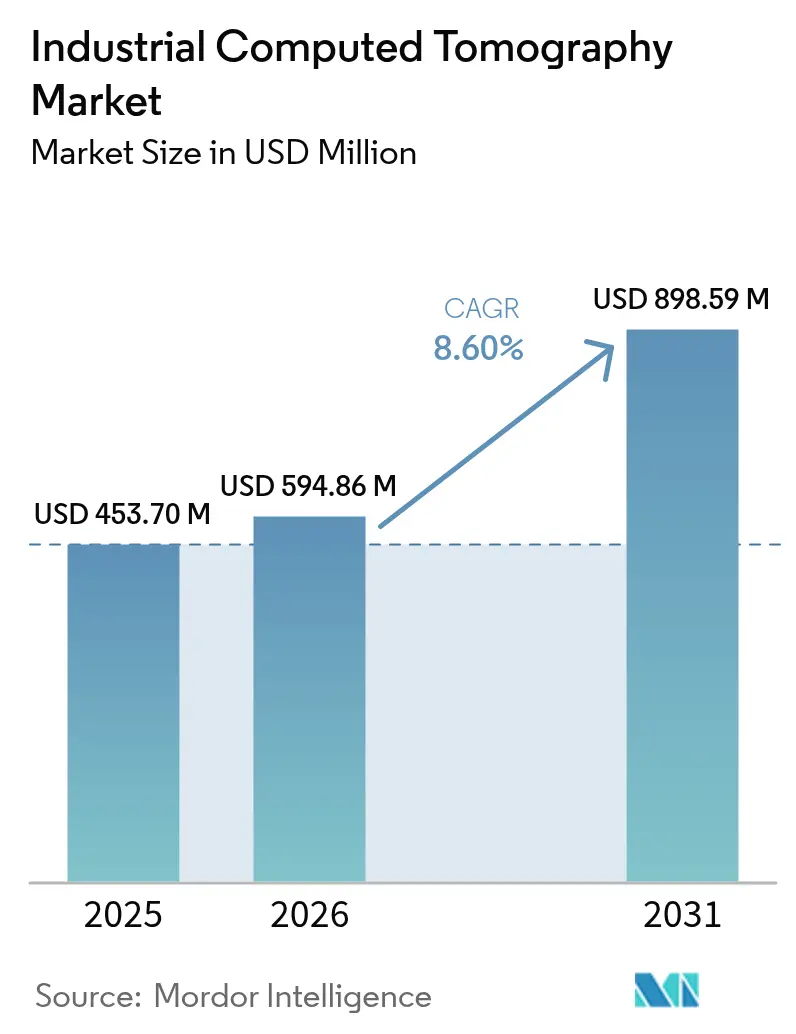
| Market Size (2026) | USD 594.86 Million |
| Market Size (2031) | USD 898.59 Million |
| Growth Rate (2026 - 2031) | 8.60% CAGR |
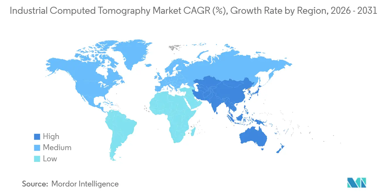
| Fastest Growing Market | Asia Pacific |
| Largest Market | Asia Pacific |
| Market Concentration | Medium |
Major Players *Disclaimer: Major Players sorted in no particular order Image © Mordor Intelligence. Reuse requires attribution under CC BY 4.0. | |
Industrial Computed Tomography Market Analysis by Mordor Intelligence
The industrial computed tomography market size is expected to increase from USD 543.70 million in 2025 to USD 594.86 million in 2026 and reach USD 898.59 million by 2031, growing at a CAGR of 8.6% over 2026-2031. Growing preference for inline volumetric inspection, rapid detector innovations, and artificial-intelligence reconstruction engines are reshaping quality-assurance practices in aerospace, automotive, electronics, and medical-device production. High-voltage platforms remain essential for thick-wall castings, yet low-medium voltage systems are expanding swiftly as semiconductor packaging and micro-electronics manufacturers prioritize compact footprints. Cone-beam technology dominates adoption because single-rotation acquisitions compress scan cycles to well under 10 seconds, a prerequisite for high-volume automotive and battery lines. Geographically, China, Japan, and South Korea drive orders in Asia-Pacific, while Africa posts the fastest growth as exporters seek certification for European and North American customers.
Key Report Takeaways
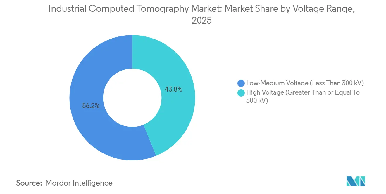
- By voltage range, high-voltage systems led with 56.19% of the industrial computed tomography market share in 2025, while low-medium voltage platforms are projected to expand at a 8.96% CAGR through 2031.
- By application, flaw detection accounted for 44.31% of 2025 revenue, whereas assembly analysis is forecast to grow at a 8.89% CAGR to 2031.
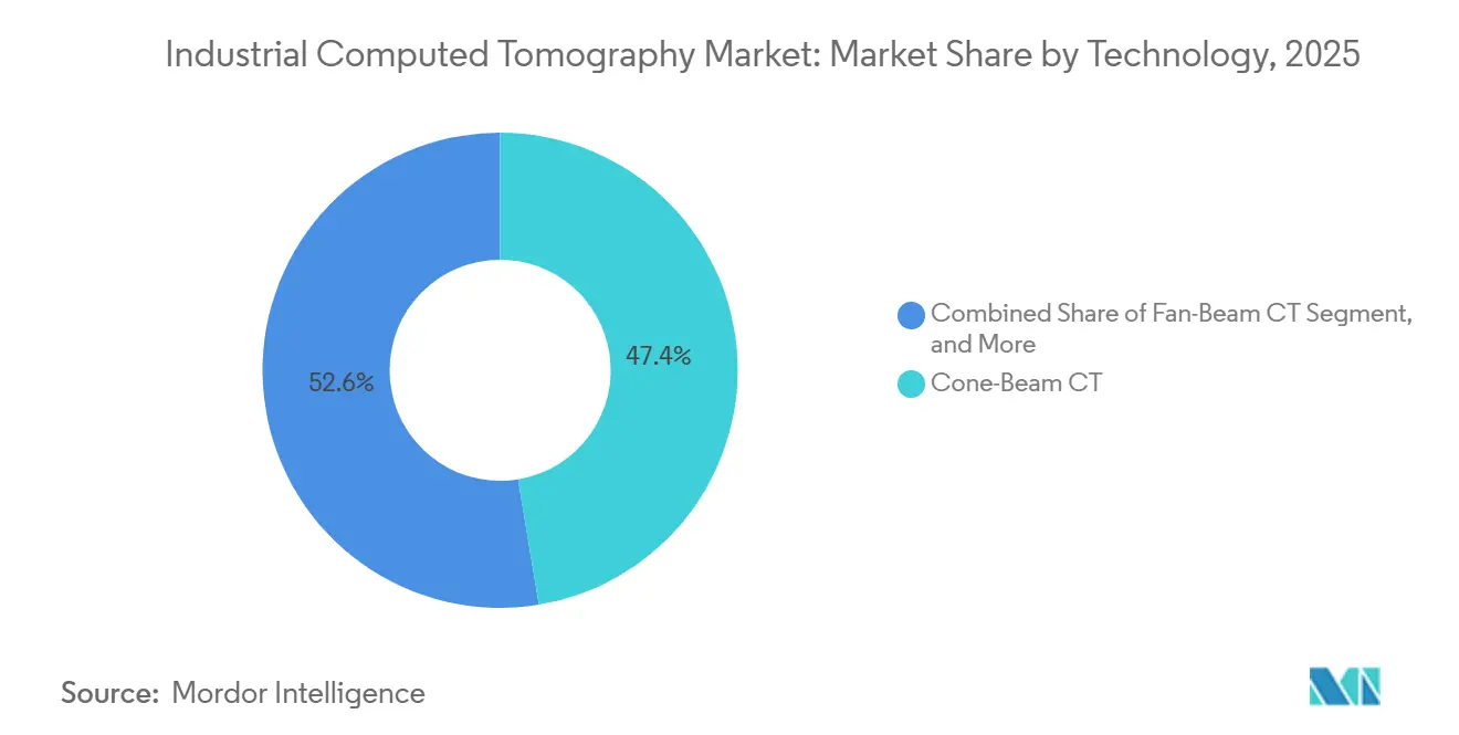
- By technology, cone-beam scanners held 47.39% of 2025 spending and are set to advance at a 9.53% CAGR during 2026-2031.
- By end-user industry, aerospace and defense represented 29.75% of demand in 2025, while medical-device manufacturers are tracking a 9.21% CAGR through 2031.
- By geography, Asia-Pacific captured 34.49% of 2025 value; the region is also poised for a 9.15% CAGR to 2031.
Note: Market size and forecast figures in this report are generated using Mordor Intelligence’s proprietary estimation framework, updated with the latest available data and insights as of 2026.
Global Industrial Computed Tomography Market Trends and Insights
Drivers Impact Analysis*
| Driver | (~) % Impact on CAGR Forecast | Geographic Relevance | Impact Timeline |
|---|---|---|---|
| Rising Demand for Non-Destructive Testing in Aerospace and Automotive | +2.10% | Global, concentrated in North America, Europe, and Asia-Pacific | Medium term (2-4 years) |
| Growing Adoption of Additive Manufacturing Quality Control | +1.80% | North America and Europe core, expanding to Asia-Pacific | Medium term (2-4 years) |
| Advances in Detector Resolution and Image Reconstruction | +1.50% | Global | Long term (≥ 4 years) |
| Miniaturization of Electronics Necessitating Micro-CT Inspection | +1.20% | Asia-Pacific core, spillover to North America | Short term (≤ 2 years) |
| AI-Driven Automated Defect Recognition Reducing Cycle Time | +1.40% | Global, early adoption in North America and Europe | Short term (≤ 2 years) |
| Battery-Safety Regulations Across Electric-Vehicle Supply Chains | +0.60% | Global, concentrated in Europe, China, and North America | Medium term (2-4 years) |
| Source: Mordor Intelligence | |||
Rising Demand for Non-Destructive Testing in Aerospace and Automotive
Aerospace original-equipment manufacturers mandate 100% volumetric inspection of safety-critical castings to comply with AS9100, replacing legacy sampling that could overlook sub-surface porosity. Turbine-blade producers now scan every airfoil to capture micro-cracks below 50 µm, a resolution conventional radiography cannot meet.[1]SAE International, “AS9100 Aerospace Quality Standards,” sae.org Automotive platforms that blend aluminium extrusions with carbon-fiber panels also need volumetric data because ultrasound coupling fails at dissimilar interfaces. Gigacast battery enclosures require exhaustive porosity mapping, prompting leading electric-vehicle makers to install inline CT cells at casting exits. The European Union Battery Regulation enforces defect traceability throughout the pack lifecycle, embedding CT data archiving into supplier contracts.
Growing Adoption of Additive Manufacturing Quality Control
Layer-by-layer deposition traps gas porosity that surface inspection misses, positioning CT as the only viable certification path for metallic additive parts. NASA’s injector-qualification program cemented 10 µm CT as a de-facto aerospace baseline. ASTM E2934, released in 2024, standardized voxel sizes and algorithms, enabling cross-laboratory correlation of powder-bed-fusion defects.[2]ASTM International, “ASTM E2934 Standard for Additive Manufacturing CT Inspection,” astm.org Medical-device firms rely on CT to verify lattice implants against design intent, ensuring osseointegration performance under FDA oversight. First-article inspection savings exceed USD 100,000 per rejected aerospace part, reinforcing CT’s role in additive-manufacturing workflows.
AI-Driven Automated Defect Recognition Reducing Cycle Time
Manual slice review historically limited throughput to 10–15 parts per shift, but deep-learning models now deliver 82% intersection-over-union on porosity segmentation, automating pass-fail calls. ZEISS Automated Defect Detection trims false positives by 60% in die-casting lines.[3]ZEISS, “Automated Defect Detection for Industrial CT,” zeiss.com Nikon’s December 2025 AI Reconstruction cuts turbine-blade scan time from 45 minutes to 90 seconds by predicting missing angles. Oak Ridge’s Simurgh framework demonstrates 12-20× faster reconstruction on GPU clusters, delivering fourfold accuracy gains, and is being commercialized by multiple vendors. Integrated edge computing now triggers automatic part ejection within 5 seconds of scan completion on battery lines.
Battery-Safety Regulations Across Electric-Vehicle Supply Chains
UNECE Regulation 100.03 compels thermal-propagation tests for lithium-ion packs and indirectly mandates CT verification of busbar welds and cell-spacing uniformity. China’s GB 38031 obliges suppliers to document internal defect populations, accelerating micro-CT deployments at domestic cell factories. Phase-contrast CT is emerging to visualize dendrite growth in solid-state designs, a metric unavailable to conventional absorption imaging. The European Battery Alliance positions internal-defect characterization as essential for second-life certification, sustaining used-system demand among recyclers.
High Acquisition and Operating Cost of High-Power CT Systems
Penetrating 300 mm steel requires 450 kV platforms priced up to USD 2 million, excluding annual service contracts that add 15-20% of capital outlay. Reinforced-concrete bunkers exceeding 1 m walls can push facility upgrades above USD 500,000 and extend deployment by a year. Subscription models, such as Lumafield’s USD 3,000-per-month offering, lower the entry barrier but cap penetration depth at aluminium components due to 150 kV tubes. The absence of standardized ROI calculators prolongs procurement cycles, especially for small-batch contract manufacturers.
Radiation-Safety Compliance Burden and Facility Upgrades
IEC 61010 mandates annual dose surveys and interlocked shielding, imposing recurrent costs on small shops. EU Directive 2013/59/Euratom obliges employers to archive dose records for 30 years, escalating administrative overhead. In the United States, Nuclear Regulatory Commission licensing can stretch to 18 months, delaying revenue realization for service bureaus. Enhanced shielding above 200 kV adds USD 200,000-400,000 in retrofit expense, while a shrinking pool of certified radiographers pushes wages up 8% annually in North America.
*Our forecasts treat driver/restraint impacts as directional, not additive. The impact forecasts reflect baseline growth, mix effects, and variable interactions.
Segment Analysis
By Voltage Range: Compact Systems Gain Traction
Low-medium voltage units below 300 kV are projected to outpace the broader industrial computed tomography market at a 9.96% CAGR as electronics and medical-device producers favour benchtop formats requiring only lead-lined cabinets for compliance. Conversely, high-voltage scanners retained 56.19% of 2025 revenue because aerospace foundries still need 450 kV penetration for titanium castings.
Regulatory pressure also shapes buying patterns: systems above 200 kV face stricter IEC 61010 interlock requirements, adding USD 100,000 in hardware while stretching commissioning by six months. Micro-CT platforms under 100 kV continue carving niches in semiconductor packaging, where 1 µm resolution identifies void clusters within solder balls. Carbon-nanotube sources operating at 150 kV promise 225 kV-class penetration with instant-on tubes, signalling potential realignment of voltage-range preferences after 2028.


By Application: Assembly Verification Accelerates
Assembly analysis, projected to post a 9.89% CAGR, is emerging as the fastest-growing application. Electric-vehicle producers now inspect busbar welds and thermal-interface-material coverage in three-second cycles, embedding CT directly onto battery lines. Flaw detection anchored 44.31% of 2025 spending, with established acceptance criteria in turbine-blade and aluminium-casting programs.
AI classifiers embedded in flaw-detection workflows reduce false positives by 60%, allowing aerospace suppliers to tighten acceptance thresholds without higher scrap rates. Failure-analysis adoption is also broadening because warranty costs push automakers to CT-scan returned components, correlating defect signatures with supplier deviations. Adoption of phase-contrast CT in research environments visualizes crack-tip stress fields for in-depth forensic studies.
By Technology: Cone-Beam Dominance Persists
Cone-beam systems captured 47.39% of revenue in 2025 and are expanding at 9.53% through 2031 as high-dynamic-range flat-panel detectors enable single-rotation scans that finish in under 10 seconds. Fan-beam architectures, though slower, remain indispensable where isotropic voxel resolution under 5 µm is mandatory, especially for turbine-blade metrology.
Iterative reconstruction algorithms suppress metal artifacts in cone-beam images, delivering 30-fold cycle-time reductions without compromising defect sensitivity. Laminography continues to serve flat-panel PCB inspection, mitigating scatter from multilayer copper traces. Photon-counting detectors that bucket X-ray energies into discrete channels will soon allow single-scan material discrimination, expanding cone-beam applicability into composite interiors.

By End-User Industry: Medical Devices Surge
Medical-device manufacturers are poised for a 9.21% CAGR as ISO 13485 traceability rules tighten and patient-matched implants require 100%-dimensional verification. Aerospace and defense retained 29.75% of demand in 2025, sustained by AS9100 mandates for volumetric inspection of safety-critical castings.
Automotive battery-pack assemblers integrate inline CT at casting exits to detect gigacast porosity in near-real time, cutting scrap detection from days to seconds. Electronics manufacturers deploy sub-micrometer micro-CT to inspect ball-grid arrays, because conventional radiography cannot detect voiding below 10%. Academic institutes leverage in-situ CT for materials research, seeding industrial best practices in future standards.
Geography Analysis
Asia-Pacific held 34.49% of 2025 revenue, anchored by China’s subsidized casting-inspection upgrades under the 14th Five-Year Plan, Japan’s 50% grant for semiconductor micro-CT, and South Korea’s shipbuilding mandates for LNG carrier welds. Suppliers such as BYD and SAIC now deploy inline CT on battery lines, while Japanese electronics corridors scan every ball-grid array before substrate attach.
North America maintains solid demand, driven by FAA additive-manufacturing guidance and battery gigafactory buildouts. Tesla, General Motors, and Ford each operate multiple inline CT cells, and Canada’s Montreal cluster houses service bureaus supporting Pratt and Whitney and Bombardier suppliers. Licensing delays at the Nuclear Regulatory Commission remain a deployment bottleneck, though reciprocity agreements are easing interstate transfers.
Middle East and Africa, albeit from a small base, is the fastest-growing geography with a 5.15% CAGR as South African mining-equipment exporters and Nigerian oil-and-gas component shops adopt CT to meet European and API standards. BMW and Mercedes-Benz assembly plants in Pretoria now require volumetric porosity reports from local foundries, while Kenya pilot’s turbine-blade scans to service regional carriers.

Competitive Landscape
The top five vendors ZEISS, Nikon Metrology, Baker Hughes Waygate Technologies, Yxlon International, and North Star Imaging collectively hold roughly 45-50% share, characterizing the industrial computed tomography market as moderately concentrated. Competitive focus is shifting from hardware to AI-enabled reconstruction and automated defect detection: Nikon’s AI Reconstruction enables 30-fold scan-time reductions, while ZEISS defect analytics cut false positives by 60% in die-casting lines.
Chinese suppliers such as Sanying Precision and Seamark ZM offer 225 kV systems at 40-50% discounts but face export hurdles over detector consistency and after-sales support. Subscription-based newcomers like Lumafield lower capital barriers with USD 3,000-per-month scanners bundled with cloud reconstruction, targeting job shops and product-development teams.
Mergers and technology alliances accelerate capability building: Comet Group’s EUR 85 million (USD 90 million) detector acquisition vertically integrates Yxlon, while Baker Hughes partners with AI start-ups to embed real-time classification into Waygate platforms. Vendors increasingly bundle operator training to address the global shortage of certified radiographers, creating sticky service revenue streams.
Industrial Computed Tomography Industry Leaders
Baker Hughes Company (Waygate Technologies)
Carl Zeiss AG
Nikon Corporation – Nikon Metrology NV
Comet Group – Yxlon International GmbH
Wenzel Group GmbH and Co. KG
- *Disclaimer: Major Players sorted in no particular order


Recent Industry Developments
- September 2025: Nikon Metrology opened a USD 30 million plant in Tennessee to localize production of cone-beam CT tubes for U.S. aerospace and automotive clients. The move shortens lead times to eight weeks and sidesteps the volatility of trans-Pacific freight.
- April 2025: Carl Zeiss unveiled the VoluMax Ultra, a high-throughput CT cell equipped with dual-energy sources and AI-driven defect mapping, targeting battery-cell lines at 15 ppm yield targets. The launch aims to convert EV suppliers that are reliant on 2D radiography.
- February 2025: Lumafield introduced Nebula Cloud, a SaaS analytics suite offering automated CAD-to-CT deviation reports, creating a recurring-revenue layer atop its desktop hardware base.
- December 2024: Waygate Technologies partnered with BMW to pilot in-line CT at the automaker’s German EV battery plant, integrating robotic loading and 30-second scan cycles for prismatic cells.


Global Industrial Computed Tomography Market Report Scope
The Industrial Computed Tomography Market Report is Segmented by Voltage Range (Low-Medium Voltage, High Voltage), Application (Flaw Detection, Failure Analysis, Assembly Analysis, Other Applications), Technology (Fan-Beam CT, Cone-Beam CT, Others), End-User Industry (Aerospace and Defense, Automotive, Electronics and Semiconductors, Medical Devices, Academic and Research Institutes, Other Industries), and Geography (North America, South America, Europe, Asia-Pacific, Middle East, Africa). The Market Forecasts are Provided in Terms of Value (USD).
By Voltage Range
| Low-Medium Voltage (Less Than 300 kV) |
| High Voltage (Greater Than or Equal To 300 kV) |
By Application
| Flaw Detection / Inspection |
| Failure Analysis |
| Assembly Analysis |
| Other Applications |
By Technology/Scanning Technique
| Fan-Beam CT |
| Cone-Beam CT |
| Others Technology/Scanning Technique |
By End-User Industry
| Aerospace and Defense |
| Automotive |
| Electronics and Semiconductors |
| Medical Devices |
| Academic and Research Institutes |
| Other End-User Industry |
By Geography
| North America | United States |
| Canada | |
| Mexico | |
| South America | Brazil |
| Argentina | |
| Rest of South America | |
| Europe | Germany |
| United Kingdom | |
| France | |
| Italy | |
| Spain | |
| Russia | |
| Rest of Europe | |
| Asia-Pacific | China |
| Japan | |
| India | |
| South Korea | |
| Rest of Asia-Pacific | |
| Middle East | Saudi Arabia |
| United Arab Emirates | |
| Turkey | |
| Rest of Middle East | |
| Africa | South Africa |
| Nigeria | |
| Rest of Africa |
| By Voltage Range | Low-Medium Voltage (Less Than 300 kV) | |
| High Voltage (Greater Than or Equal To 300 kV) | ||
| By Application | Flaw Detection / Inspection | |
| Failure Analysis | ||
| Assembly Analysis | ||
| Other Applications | ||
| By Technology/Scanning Technique | Fan-Beam CT | |
| Cone-Beam CT | ||
| Others Technology/Scanning Technique | ||
| By End-User Industry | Aerospace and Defense | |
| Automotive | ||
| Electronics and Semiconductors | ||
| Medical Devices | ||
| Academic and Research Institutes | ||
| Other End-User Industry | ||
| By Geography | North America | United States |
| Canada | ||
| Mexico | ||
| South America | Brazil | |
| Argentina | ||
| Rest of South America | ||
| Europe | Germany | |
| United Kingdom | ||
| France | ||
| Italy | ||
| Spain | ||
| Russia | ||
| Rest of Europe | ||
| Asia-Pacific | China | |
| Japan | ||
| India | ||
| South Korea | ||
| Rest of Asia-Pacific | ||
| Middle East | Saudi Arabia | |
| United Arab Emirates | ||
| Turkey | ||
| Rest of Middle East | ||
| Africa | South Africa | |
| Nigeria | ||
| Rest of Africa | ||


Key Questions Answered in the Report
How fast is inline CT scanning in modern battery lines?
Edge-enabled cone-beam systems now complete pouch-cell weld inspection in about 3 seconds, matching automotive assembly takt times.
What makes cone-beam CT the dominant technology?
Single-rotation acquisition captures an entire part volume quickly, and iterative reconstruction suppresses artifacts, yielding sub-10-second scans for automotive castings.
Why are medical-device firms increasing CT adoption?
ISO 13485 traceability rules and the rise of patient-matched implants require 100% volumetric verification of internal geometries.
Which regions are growing the quickest in CT adoption?
Asia-Pacific posts a 9.15% CAGR through 2031 as exporters seek certification for European and North American markets.
How does AI reduce CT inspection cycle times?
Deep-learning models reconstruct missing angles and classify defects automatically, cutting blade scans from 45 minutes to 90 seconds and slashing manual review hours.
What cost barriers limit high-voltage CT deployment?
Acquisition prices up to USD 2 million plus reinforced-concrete shielding and yearly service contracts raise total cost of ownership beyond many small manufacturers.
Page last updated on:


