Hybrid Memory Cube Market Size and Share
Market Overview
| Study Period | 2020 - 2031 |
|---|---|
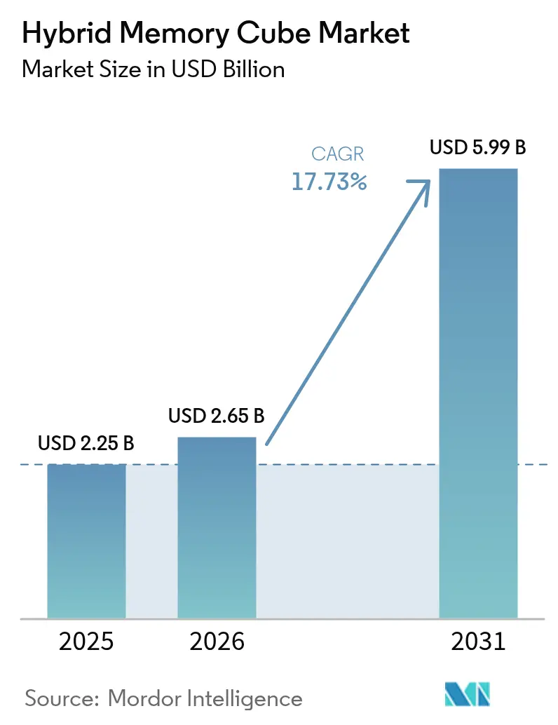
| Market Size (2026) | USD 2.65 Billion |
| Market Size (2031) | USD 5.99 Billion |
| Growth Rate (2026 - 2031) | 17.73% CAGR |
| Fastest Growing Market | Asia Pacific |
| Largest Market | Asia Pacific |
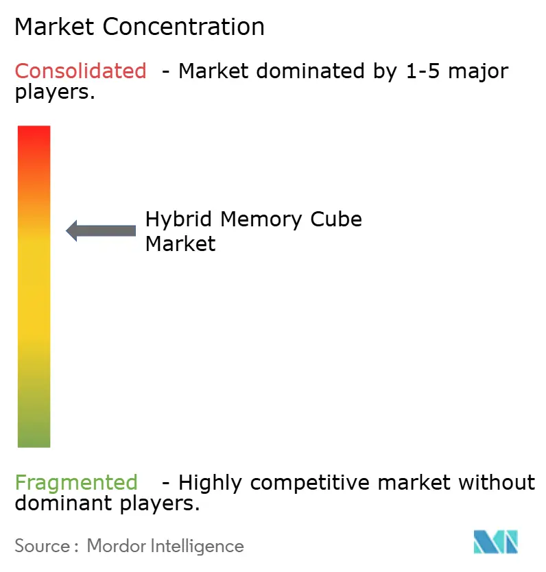
| Market Concentration | Medium |
Major Players *Disclaimer: Major Players sorted in no particular order Image © Mordor Intelligence. Reuse requires attribution under CC BY 4.0. | |
Hybrid Memory Cube Market Analysis by Mordor Intelligence
The Hybrid Memory Cube market size is expected to grow from USD 2.25 billion in 2025 to USD 2.65 billion in 2026 and is forecast to reach USD 5.99 billion by 2031 at 17.73% CAGR over 2026-2031. Enterprise storage upgrades, chiplet-based heterogeneous integration, and the rollout of exascale supercomputers are widening the total addressable opportunity, while the manufacturing scale in the Asia-Pacific positions the region at the center of supply and demand. Technology competition is intensifying as optical-interconnect prototypes and universal chiplet interconnect standards reduce vendor lock-in and expand the potential customer base. At the same time, yield headwinds in through-silicon-via (TSV) processes and thermal-management complexity threaten to restrain near-term unit cost improvements.
Key Report Takeaways
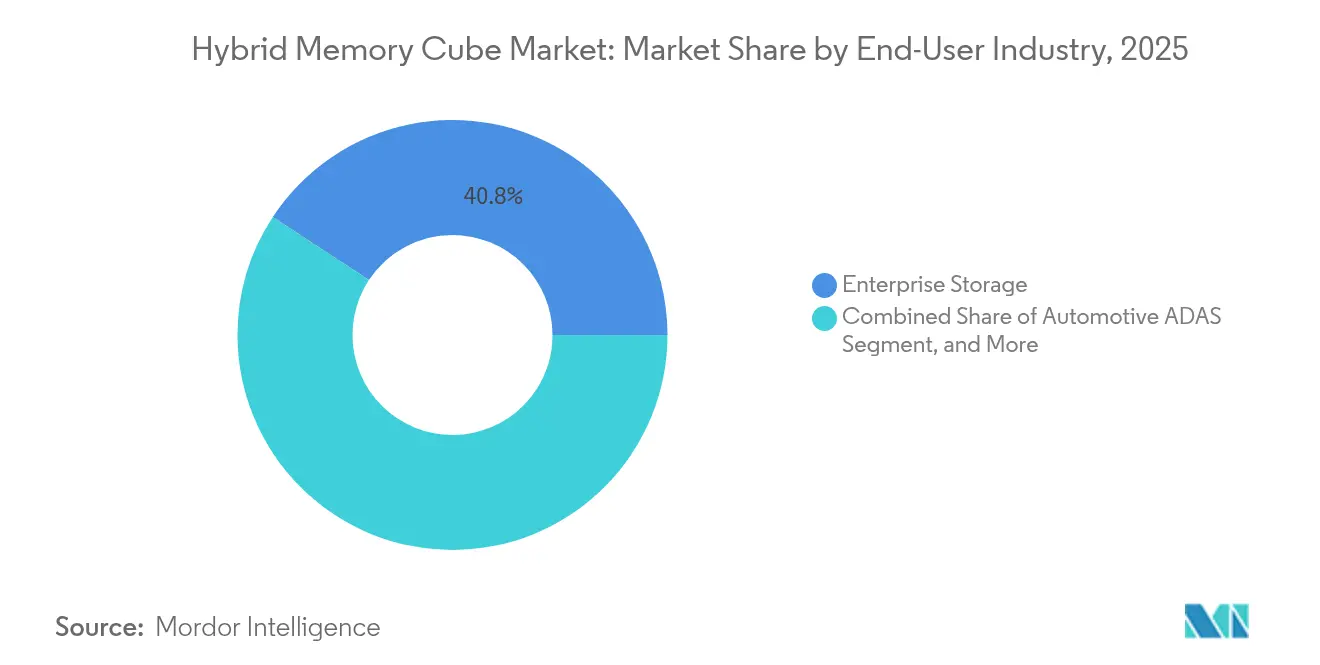
- By end-user industry, enterprise storage led with a 40.75% market share of the hybrid memory cube market in 2025, whereas automotive ADAS is forecast to expand at a 20.42% CAGR through 2031.
- By memory capacity, the 16 GB to 32 GB tier accounted for 37.15% of the hybrid memory cube market share in 2025. Modules larger than 32 GB are expected to grow at a 19.62% CAGR to 2031.
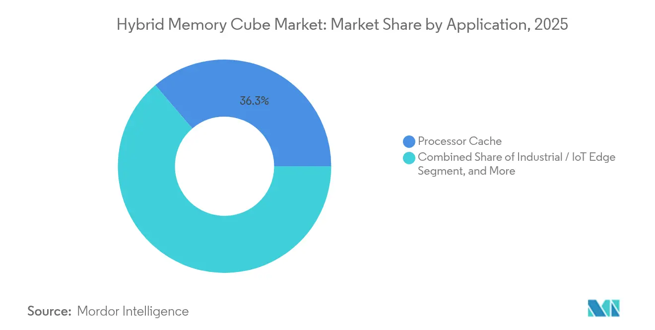
- By application, processor-cache deployments accounted for 36.25% of the hybrid memory cube market size in 2025, and industrial and IoT edge nodes are projected to advance at a 20.15% CAGR during 2026-2031.
- By technology node, TSV-based second-generation products commanded a 47.35% of the hybrid memory cube market share in 2025; however, optical-interconnect variants are projected to advance at a 19.28% CAGR over the forecast horizon.
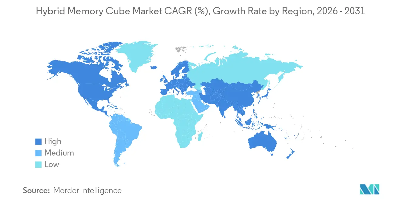
- By geography, the Asia-Pacific region contributed 41.05% of the hybrid memory cube market share in 2025 and is projected to grow at a 19.93% CAGR through 2031, outpacing all other regions.
Note: Market size and forecast figures in this report are generated using Mordor Intelligence’s proprietary estimation framework, updated with the latest available data and insights as of 2026.
Global Hybrid Memory Cube Market Trends and Insights
Drivers Impact Analysis*
| Driver | (~) % Impact on CAGR Forecast | Geographic Relevance | Impact Timeline |
|---|---|---|---|
| Rapid uptake of AI / HPC workloads demanding high-bandwidth memory | +4.2% | Global, with concentration in North America and Asia Pacific | Medium term (2-4 years) |
| Growing enterprise storage and hyperscale datacenter refresh cycles | +3.8% | North America and Europe, spill-over to Asia Pacific | Short term (≤ 2 years) |
| Expanding 5G core and edge networking equipment deployments | +2.5% | Asia Pacific core, spill-over to Middle East and Africa | Medium term (2-4 years) |
| Government-backed exascale computing initiatives in the United States, China and Europe | +2.9% | United States, China, European Union | Long term (≥ 4 years) |
| Chiplet-based heterogeneous integration architectures gaining traction | +2.7% | Global, with early gains in Taiwan, South Korea, United States | Medium term (2-4 years) |
| Shift toward composable and disaggregated server architecture in cloud platforms | +2.1% | North America and Europe hyperscale operators | Long term (≥ 4 years) |
| Source: Mordor Intelligence | |||
Rapid Uptake of AI and HPC Workloads Demanding High-Bandwidth Memory
Large-language-model training has underscored the memory wall, where compute stalls before arithmetic units saturate, and Hybrid Memory Cube packages deliver up to 320 GB/s to keep GPUs and tensor cores fed.[1]Institute of Electrical and Electronics Engineers, “Energy Efficiency in 3-D Memory Interconnects,” ieee.org Edge inference for real-time language translation and autonomous perception now mandates low-latency DRAM alternatives, cementing demand for vertically stacked memory. Micron reported that AI server memory content doubled relative to traditional enterprise nodes in fiscal 2024, with high-bandwidth products capturing a rising percentage mix. IEEE research has found that 3-D interconnects lower energy per bit by 40% compared to DDR5, thereby reducing operating costs in megawatt-scale clusters. Continuous fine-tuning and retrieval-augmented generation extend memory footprints beyond terabyte levels, and modular scalability makes Hybrid Memory Cube attractive for such regimes. Early adopters also note latency determinism advantages, which improve quality-of-service metrics for conversational AI workloads.
Growing Enterprise Storage and Hyperscale Datacenter Refresh Cycles
Hyperscalers are replacing HDD arrays with all-flash nodes that integrate computational storage processors, and these chips demand bandwidth to manage parallel NAND channels with minimal queue depth.[2]Intel Corporation, “Investor Presentation 2024,” intc.com Intel highlighted that next-generation storage controllers rely on high-bandwidth memory to accelerate inline deduplication, erasure coding, and encryption. Enterprise refresh cycles are compressing as organizations adopt composable infrastructure, further emphasizing the need for packet-based memory interfaces that Hybrid Memory Cube supports. Samsung disclosed that enterprise SSD attach rates for stacked memory doubled year-over-year in 2024, reflecting this migration. Regulatory frameworks such as ISO 27001 intensify bandwidth needs by requiring always-on encryption and audit logging. Hyperscale operators also seek ways to reduce total rack count, and high-bandwidth memory reduces per-node latency, enabling denser deployments.
Government-Backed Exascale Computing Initiatives in the United States, China, and Europe
The U.S. Department of Energy’s Frontier and Aurora systems achieve sustained exaflop performance by utilizing 3D stacked memory, which provides consistent bandwidth to thousands of accelerators. China’s National Supercomputing Centers in Wuxi and Guangzhou deployed pilot systems with domestic stacked memory to sidestep import risks, backed by the National Integrated Circuit Fund’s CNY 15 billion allocation in 2024. The EuroHPC Joint Undertaking earmarked EUR 1.2 billion for pre-exascale projects, specifying high-bandwidth modules that support coherent interconnects and dynamic voltage scaling. These public investments offset non-recurring engineering costs, enabling commercial vendors to refine products before volume rollouts. Export-control regimes further accelerate domestic technology development in China, positioning Hybrid Memory Cube as a hedge against supply-chain shocks. Vendors that secure reference design wins now can establish long-cycle revenue streams once systems graduate from pilot to production.[3]Samsung Electronics, “Enterprise SSD Roadmap 2024,” samsung.com
Chiplet-Based Heterogeneous Integration Architectures Gaining Traction
Chiplet design splits complex SoCs into smaller dies, allowing economical node mixing and yield improvements. AMD’s EPYC roadmap features stacked memory dies connected through organic interposers, showcasing the advantages of TSV and chip-on-wafer-on-substrate technologies. TSMC expanded chip-on-wafer capacity in 2024, enabling customers to integrate Hybrid Memory Cube with logic or analog chiplets in a single package. The Universal Chiplet Interconnect Express (UCIe) standard, finalized in 2024, defines electrical, protocol, and mechanical specifications that the Hybrid Memory Cube serializer-deserializer already meets, lowering adoption friction. IEEE Spectrum estimated that chiplet segmentation reduces mask costs by 30% and localizes yield excursions, thereby improving the economic viability of mid-volume applications. Automotive and aerospace customers gain the flexibility to pair safety-certified compute chiplets with high-bandwidth memory modules, thereby speeding up platform certification cycles.
Restraints Impact Analysis*
| Restraint | (~) % Impact on CAGR Forecast | Geographic Relevance | Impact Timeline |
|---|---|---|---|
| Strong incumbency of conventional DDRx / LPDDR DRAM technology | -2.4% | Global | Short term (≤ 2 years) |
| High manufacturing cost and TSV yield constraints | -3.1% | Global, acute in leading-edge fabs | Medium term (2-4 years) |
| Thermal management complexity in 3-D stacked memory cubes | -1.8% | North America and Europe datacenter operators | Medium term (2-4 years) |
| Limited supplier ecosystem and IP licensing frictions | -1.5% | Global, with friction in Asia Pacific and Europe | Long term (≥ 4 years) |
| Source: Mordor Intelligence | |||
High Manufacturing Cost and TSV Yield Constraints
Deep reactive-ion etching for TSVs introduces defect mechanisms not present in planar DRAM, increasing the per-gigabyte cost by up to 60% relative to DDR5, according to SK hynix’s 2024 earnings call. Yields under 85% create redundancy overhead and inflate die area, reducing gross margins. Copper-pumping failures during thermal cycling further damage bond integrity, worsening scrap rates in advanced packaging lines. Each TSV-capable cleanroom retrofit costs at least USD 500 million and needs nearly two years to qualify, limiting rapid capacity expansion. Environmental directives such as the EU’s RoHS add material-substitution requirements, complicating process chemistry and further delaying scale-up. Until yield climbs above 90%, vendors are likely to focus on premium niches rather than mass-market volumes.
Strong Incumbency of Conventional DDRx and LPDDR Technology
DDR5 module shipments surpassed 200 million units in 2023, driving per-gigabyte cost below USD 3 and reinforcing supply-chain economies of scale. Server OEMs need lengthy qualification cycles to introduce a non-DDR interface, and many enterprise customers maintain risk-averse purchasing policies. LPDDR5 already delivers adequate bandwidth for mobile and automotive use, reducing the urgency to shift to stacked solutions for cost-sensitive designs. JEDEC’s DDR6 and LPDDR6 roadmaps extend incumbent trajectories through 2027, delaying platform architects’ need for disruptive memory adoption. The comfort of a familiar ecosystem means many buyers will wait for stacked-memory prices to converge before committing to a design overhaul.
*Our forecasts treat driver/restraint impacts as directional, not additive. The impact forecasts reflect baseline growth, mix effects, and variable interactions.
Segment Analysis
By End-User Industry: Enterprise Storage Holds Lead, Automotive ADAS Accelerates
Enterprise storage contributed 40.75% of 2025 revenue, underpinned by hyperscale operators refreshing all-flash arrays with memory-semantic storage controllers. These upgrades increase random-access throughput and use Hybrid Memory Cube packages to maintain low tail latency across parallel NAND channels. Automotive ADAS workloads, centered on Level 3 and Level 4 autonomy, are projected to rise at a 20.42% CAGR through 2031 as sensor fusion and in-vehicle AI become mainstream. Telecommunications, high-performance computing, and industrial automation each adopt the Hybrid Memory Cube to address deterministic latency needs that outstrip those of conventional DRAM. Regulatory requirements surrounding functional-safety certification and cybersecurity accelerate procurement in safety-critical domains.
Automotive growth highlights the shift of the hybrid memory cube market toward edge devices, which prioritize thermal efficiency and sustained bandwidth. The sensor count per vehicle is climbing, and real-time perception algorithms benefit directly from low-latency memory. Enterprise storage growth is now moderating as penetration reaches mature levels in North America and Europe, though ongoing capacity optimization ensures continued product cycles. Telecommunications operators are leveraging pooled-memory constructs in 5G core deployments. Government policies, such as the FCC’s Open RAN push and the EU Machinery Regulation, also champion modular memory architectures that Hybrid Memory Cube supports.


By Memory Capacity: Mid-Range Dominates, High-Capacity Surges
Modules in the 16 GB to 32 GB range captured 37.15% of 2025 deployments, aligning with expectations for dual-socket servers and providing the optimal sweet spot for cost-performance balance. The hybrid memory cube market size for capacities greater than 32 GB is forecast to expand at a 19.62% CAGR as large-language-model inference nodes and NUMA systems deploy multi-terabyte pools. The 8 GB-to-16 GB tier supports power-constrained edge servers, while devices with capacities below 8 GB remain common in embedded industrial controls, where radiation tolerance and extended temperature ratings take precedence over raw capacity.
The average memory per socket has doubled from 128 GB in 2020 to 256 GB in 2024, and the shift toward AI inference servers that store model weights in system memory has widened the addressable high-capacity segment. Network-slice orchestration functions in 5G cores further raise per-node capacity needs. Functional-safety and cybersecurity standards effectively double usable memory to accommodate redundancy and parity, reinforcing the case for moving up to larger HMC packages in control-plane equipment.
By Application: Processor Cache Leads, Industrial and IoT Edge Ramps Up
Processor cache usage accounted for 36.25% of 2025 deployments, providing near-memory acceleration for multi-chip server processors. Industrial and IoT edge adoption is forecast to grow at a 20.15% CAGR, as deterministic real-time workloads in factory automation and smart grid nodes require microsecond responses under harsh conditions. Data-buffer applications in storage controllers and network interface cards select Hybrid Memory Cube for queue-depth reduction, while graphics-driven systems in professional visualization leverage its bandwidth for detailed rendering.
As DDR5 narrows the bandwidth-per-pin gap, cache-oriented use cases will stabilize; however, edge-node deployment of AI analytics will sustain incremental volume growth. The advent of PCIe 5.0 and CXL 2.0 exposes memory-semantic interfaces where packetized protocols align neatly with HMC capability. Cybersecurity standards such as IEC 62443 consume extra bandwidth for secure boot and runtime attestation, indirectly boosting demand for high-bandwidth memory modules.
By Technology Node: TSV Gen 2 Leads, Optical Interconnect Gains Momentum
TSV-based Gen 2 designs held a 47.35% share in 2025 owing to supply maturity at Samsung, SK hynix, and Micron. Optical-interconnect variants are tracking a 19.28% CAGR as silicon photonics integrates more efficiently and lowers crosstalk in rack-scale disaggregated designs. Chiplet-oriented Hybrid Memory Cube devices offer a cost-efficient middle ground for mid-bandwidth applications that do not require full TSV throughput.
GPU accelerators have historically driven TSV growth; however, the emerging optical baseline may redefine package-level performance by reducing latency and lowering power per bit. Intel’s Falcon Shores integrates optical links to connect memory dies across a package boundary, signifying a production shift toward photonic methodologies. UCIe ratification reduces interface uncertainty and encourages multi-vendor chiplet ecosystems. Sustainability frameworks reward lower energy profiles, benefiting optical nodes that deliver and support regulatory compliance objectives across major regions.
Geography Analysis
The Asia Pacific delivered 41.05% of the hybrid memory cube market revenue in 2025 and is projected to grow at a 19.93% CAGR to 2031, driven by concentrated fabrication capacity at Samsung and SK hynix, as well as pro-semiconductor policies in China, Japan, South Korea, and India. The Chinese government's funds, totaling CNY 15 billion in 2024, target domestic stacked-memory innovation, while Japanese co-investment supports chiplet packaging through 2-nm nodes. Indian hyperscalers are drafting regional language AI models that require high-bandwidth memory, advancing in-country demand. Taiwan’s wafer-level packaging expansions further anchor the region as a hub for heterogeneous integration services.
North America represented 28.35% of 2025 revenue, driven by hyperscale cloud refresh cycles and the Department of Energy's exascale programs. Intel’s USD 20 billion Ohio expansion will house advanced packaging lines to embed Hybrid Memory Cube dies directly into Xeon and GPU assemblies. Amazon Web Services, Microsoft Azure, and Google Cloud all pilot disaggregated memory fabrics that pool high-bandwidth tiers across racks, a model that maximizes utilization while controlling per-server costs. Canada’s Vector and Mila institutes deploy HMC-based clusters to underpin national AI research goals. Export controls restricting advanced memory shipments reshape supply allocation patterns and drive onshore capacity investments.
Europe captured approximately 17.65% of the 2025 revenue, driven by the adoption of automotive ADAS and the installation of EuroHPC supercomputers. German tier-ones Bosch and Continental incorporated Hybrid Memory Cube into Level 3 perception platforms to meet stringent latency budgets. The region’s sovereign cloud push requires GDPR-compliant configurations, which in turn need encryption-friendly memory architectures. Arm expanded a coherent interconnect IP portfolio in 2024 to support European automotive and edge customers, underscoring local R&D momentum. The EU Chips Act funnels EUR 43 billion to double the regional semiconductor share, part of which finances advanced packaging for stacked memory lines.

Competitive Landscape
Three vertically integrated suppliers, Samsung, SK hynix, and Micron, hold more than 70% of Hybrid Memory Cube capacity, yet new entrants leverage chiplet design and optical-interconnect IP to challenge legacy incumbents. Samsung leads in optical-interconnect prototypes that embed silicon photonics with stacked dies, reducing latency by 30% compared to electrical links. Micron secured a USD 6.1 billion CHIPS Act grant to expand U.S. production, improving supply diversity. SK hynix is investing USD 4 billion to add TSV capacity, signaling confidence in the rising demand for AI accelerators.
Intel’s acquisition of photonic IP and its integration into Falcon Shores GPUs introduces a new avenue of memory supply for accelerator products. Rambus licenses high-speed serializer-deserializer blocks to chiplet designers, enabling fabless firms to incorporate HMC interfaces without analog design overhead. Cadence tools accelerate time-to-market by simulating thermal and signal integrity in 3-D packages, lowering the engineering barrier for second-tier vendors. White-space opportunities lie in automotive ADAS and industrial IoT, domains that require functional safety certification, where established DRAM vendors have limited expertise.
Technology roadmaps reveal fast iteration cycles: Samsung is sampling 36 GB optical HMC modules, Intel is staging photonic Falcon Shores for 2026, and AMD plans EPYC chiplet processors with integrated high-bandwidth memory samples in late 2025. Standardization around UCIe and ongoing JEDEC HBM4 work is expected to blur lines between stacked DRAM families and packetized Hybrid Memory Cube, possibly expanding the overall high-bandwidth memory TAM. Suppliers that secure cross-licensing agreements and align with emerging automotive cybersecurity standards will gain meaningful differentiation.
Hybrid Memory Cube Industry Leaders
Micron Technology Inc.
Intel Corporation
Samsung Electronics Co., Ltd.
SK hynix Inc.
International Business Machines Corporation
- *Disclaimer: Major Players sorted in no particular order

Recent Industry Developments
- October 2025: Samsung Electronics began mass production of 36 GB optical-interconnect memory packages at Pyeongtaek, quoting 30% lower latency than electrical SerDes equivalents.
- September 2025: SK hynix committed USD 4 billion to expand TSV fabrication lines in Icheon, with production slated for H2 2026.
- August 2025: Intel announced Falcon Shores GPU shipments with integrated photonic memory links for early 2026, initially targeting DOE exascale systems.
- July 2025: Micron won a USD 6.1 billion CHIPS Act grant to expand U.S. advanced-memory capacity, with first-phase completion expected by 2027.


Global Hybrid Memory Cube Market Report Scope
The Hybrid Memory Cube Market Report is Segmented by End-User Industry (Enterprise Storage, Telecommunications and Networking, High-Performance Computing, Automotive ADAS, Other End-Users), Memory Capacity (2 GB to 8 GB, 8 GB to 16 GB, 16 GB to 32 GB, Greater Than 32 GB), Application (Processor Cache, Data Buffer, Graphics Memory, Industrial and IoT Edge), Technology Node (TSV-based Hybrid Memory Cube Gen 2, Optical-interconnect HMC, Chiplet-based HMC), and Geography (North America, South America, Europe, Asia Pacific, Middle East and Africa). The Market Forecasts are Provided in Terms of Value (USD).
| Enterprise Storage |
| Telecommunications and Networking |
| High-Performance Computing |
| Automotive ADAS |
| Other End-User Industry |
| 2 GB–8 GB |
| 8 GB–16 GB |
| 16 GB–32 GB |
| Above 32 GB |
| Processor Cache |
| Data Buffer |
| Graphics Memory |
| Industrial / IoT Edge |
| TSV-based Hybrid Memory Cube (Gen 2) |
| Optical-interconnect HMC |
| Chiplet-based HMC |
| North America | United States | |
| Canada | ||
| Mexico | ||
| South America | Brazil | |
| Argentina | ||
| Rest of South America | ||
| Europe | Germany | |
| United Kingdom | ||
| France | ||
| Italy | ||
| Spain | ||
| Russia | ||
| Rest of Europe | ||
| Asia Pacific | China | |
| Japan | ||
| India | ||
| South Korea | ||
| Australia | ||
| Rest of Asia Pacific | ||
| Middle East and Africa | Middle East | Saudi Arabia |
| United Arab Emirates | ||
| Turkey | ||
| Rest of Middle East | ||
| Africa | South Africa | |
| Nigeria | ||
| Egypt | ||
| Rest of Africa | ||
| By End-User Industry | Enterprise Storage | ||
| Telecommunications and Networking | |||
| High-Performance Computing | |||
| Automotive ADAS | |||
| Other End-User Industry | |||
| By Memory Capacity | 2 GB–8 GB | ||
| 8 GB–16 GB | |||
| 16 GB–32 GB | |||
| Above 32 GB | |||
| By Application | Processor Cache | ||
| Data Buffer | |||
| Graphics Memory | |||
| Industrial / IoT Edge | |||
| By Technology Node | TSV-based Hybrid Memory Cube (Gen 2) | ||
| Optical-interconnect HMC | |||
| Chiplet-based HMC | |||
| By Geography | North America | United States | |
| Canada | |||
| Mexico | |||
| South America | Brazil | ||
| Argentina | |||
| Rest of South America | |||
| Europe | Germany | ||
| United Kingdom | |||
| France | |||
| Italy | |||
| Spain | |||
| Russia | |||
| Rest of Europe | |||
| Asia Pacific | China | ||
| Japan | |||
| India | |||
| South Korea | |||
| Australia | |||
| Rest of Asia Pacific | |||
| Middle East and Africa | Middle East | Saudi Arabia | |
| United Arab Emirates | |||
| Turkey | |||
| Rest of Middle East | |||
| Africa | South Africa | ||
| Nigeria | |||
| Egypt | |||
| Rest of Africa | |||


Key Questions Answered in the Report
What is the projected value of the Hybrid Memory Cube market by 2031?
The market is forecast to reach USD 5.99 billion by 2031, reflecting a 17.73% CAGR from 2026.
Which end-user sector currently contributes the most revenue?
Enterprise storage led with 40.75% of 2025 revenue as hyperscalers refreshed all-flash arrays.
Which application segment is set to grow the fastest?
Industrial-and-IoT edge nodes are expected to expand at a 20.15% CAGR during 2026-2031.
Why is Asia Pacific the fastest-growing region?
Concentrated fabrication capacity, government incentives, and strong cloud buildouts drive a 19.93% regional CAGR.
What manufacturing challenge restricts near-term cost reductions?
TSV yield rates remain below 85%, elevating per-gigabyte cost by up to 60% over DDR5 modules.
How are chiplets influencing memory adoption?
UCIe-based chiplet standards let designers integrate Hybrid Memory Cube into multi-die packages without bespoke interfaces, speeding time-to-market.
Page last updated on:


