Failure Analysis Market Size and Share
Market Overview
| Study Period | 2020 - 2031 |
|---|---|
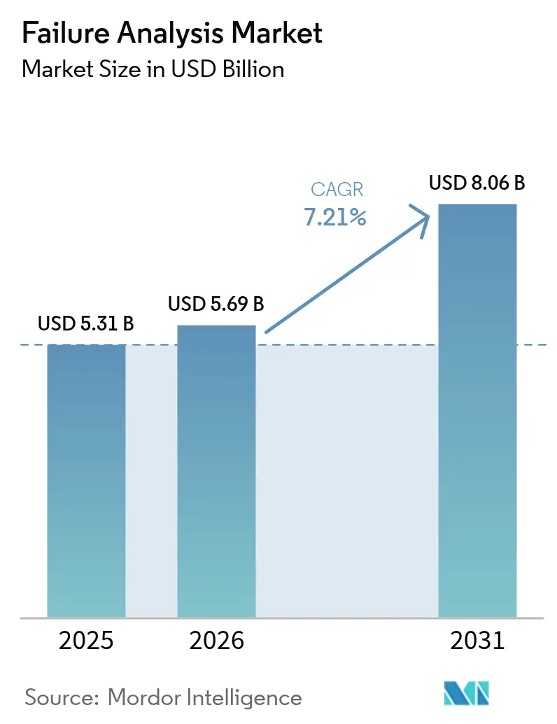
| Market Size (2026) | USD 5.69 Billion |
| Market Size (2031) | USD 8.06 Billion |
| Growth Rate (2026 - 2031) | 7.21% CAGR |
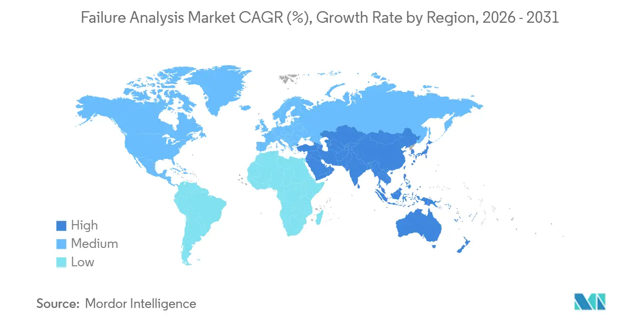
| Fastest Growing Market | Asia Pacific |
| Largest Market | Asia Pacific |
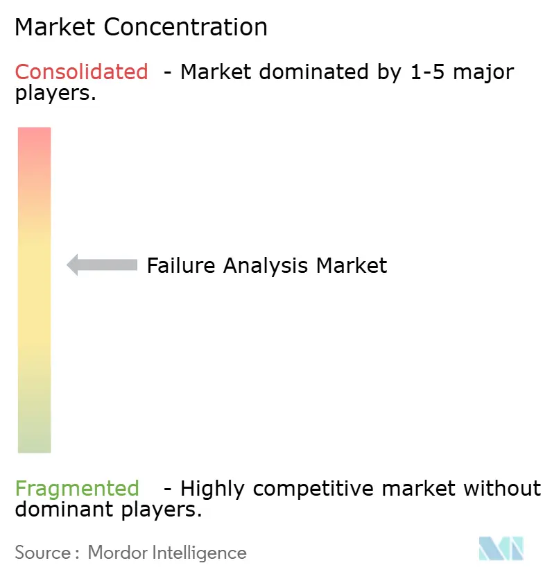
| Market Concentration | Medium |
Major Players *Disclaimer: Major Players sorted in no particular order Image © Mordor Intelligence. Reuse requires attribution under CC BY 4.0. | |
Failure Analysis Market Analysis by Mordor Intelligence
The failure analysis market size is projected to expand from USD 5.31 billion in 2025 and USD 5.69 billion in 2026 to USD 8.06 billion by 2031, registering a CAGR of 7.21% between 2026 to 2031. Asia Pacific continues to anchor demand as front-end fabs in Taiwan and South Korea raise inspection frequency to keep defect densities below 0.1 cm². Equipment vendors prioritize detector sensitivity and automation throughput, while service providers position around ISO/IEC 17025 accreditation and 24-hour turnaround. Inline metrology adoption accelerates as chipmakers race toward 2-nanometer nodes, and quantum hardware developers introduce cryogenic workflows that reposition analytical requirements. High acquisition costs remain a hurdle, yet preventive maintenance contracts gain traction because one hour of unplanned downtime can exceed USD 1 million at leading-edge fabs.
Key Report Takeaways
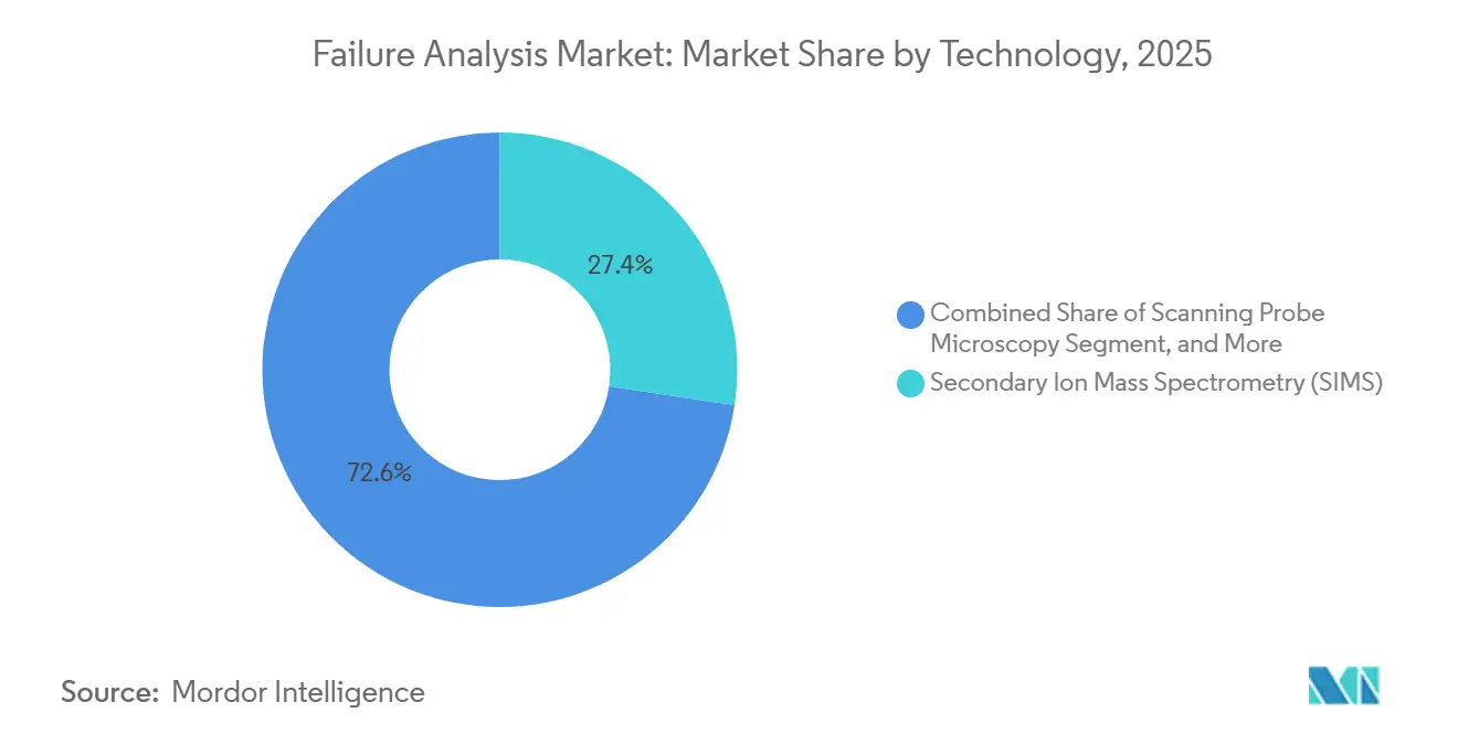
- By technology, secondary ion mass spectrometry led with 27.38% revenue share in 2025, whereas reactive ion etching is forecast to expand at an 8.27% CAGR through 2031.
- By equipment, scanning electron microscopes captured 31.41% of 2025 sales, while dual-beam systems are projected to grow at an 8.58% CAGR to 2031.
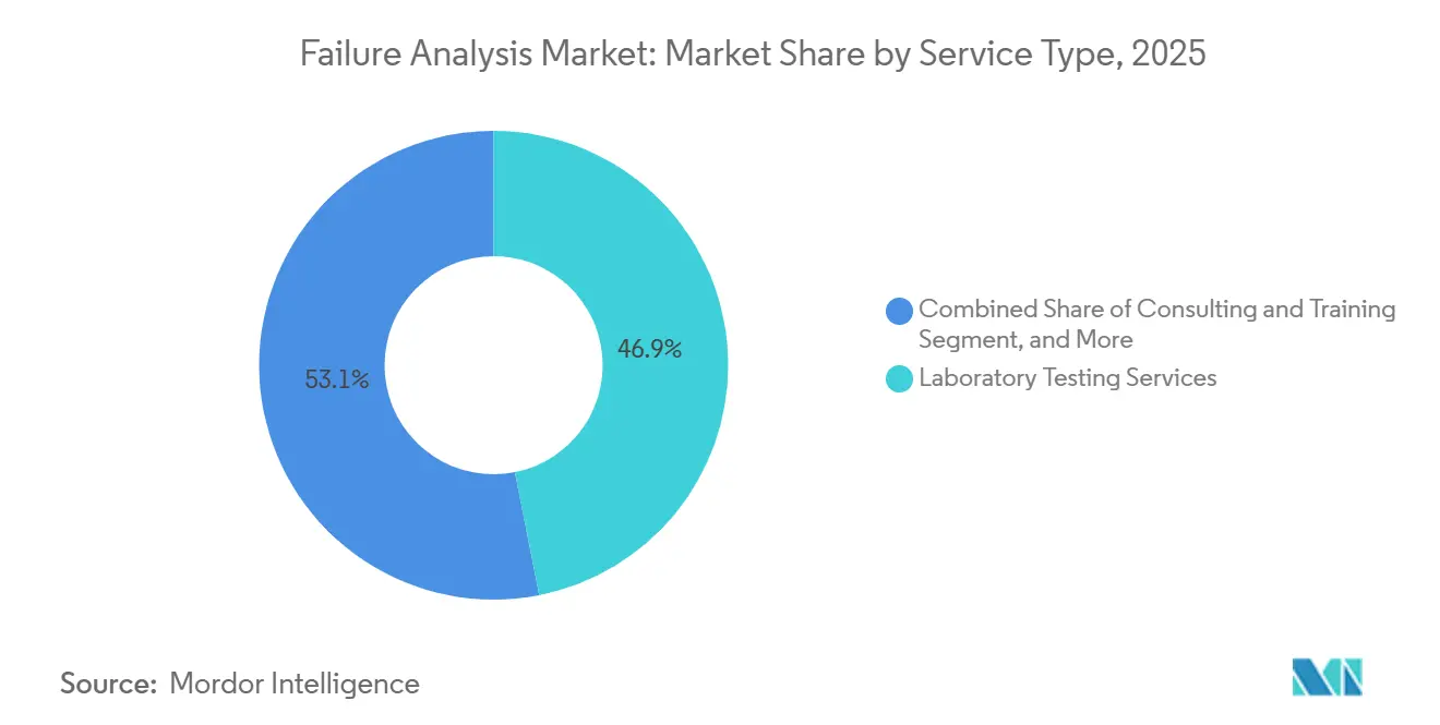
- By service type, laboratory testing commanded 46.89% revenue in 2025, yet preventive and predictive maintenance contracts are set to rise at a 9.02% CAGR during the forecast period.
- By end-user industry, electronics and semiconductors held 29.72% revenue share in 2025; quantum chip start-ups record the highest projected CAGR at 9.16% through 2031.
- By geography, Asia-Pacific accounted for 38.93% failure analysis market share in 2025 and is expected to grow at an 8.63% CAGR to 2031.
Note: Market size and forecast figures in this report are generated using Mordor Intelligence’s proprietary estimation framework, updated with the latest available data and insights as of 2026.
Global Failure Analysis Market Trends and Insights
Drivers Impact Analysis*
| Driver | (~) % Impact on CAGR Forecast | Geographic Relevance | Impact Timeline |
|---|---|---|---|
| Miniaturization of Electronic Components Boosts Demand | +1.8% | Asia Pacific core, spillover to North America | Medium term (2-4 years) |
| AI-Driven Root-Cause Analytics Adoption | +1.2% | Global, with early gains in United States, Germany, South Korea | Short term (≤ 2 years) |
| Quantum Semiconductor R&D Yield Challenges | +0.9% | North America and Europe | Long term (≥ 4 years) |
| Transition to Net-Zero Emission Manufacturing Increases Failure Criticality | +0.7% | Global, concentrated in Europe and North America | Medium term (2-4 years) |
| Technological Advancements in Failure-Analysis Tools | +0.6% | Global | Short term (≤ 2 years) |
| Innovation in Materials Design and Production Methods | +0.5% | Asia Pacific, North America | Medium term (2-4 years) |
| Source: Mordor Intelligence | |||
Miniaturization Of Electronic Components Boosts Demand
Transistor gates below 3 nanometers expose failure modes that optical tools miss, requiring transmission electron microscopes capable of 0.05 nanometer imaging to detect single-atom dopant shifts. TSMC now performs inline analysis at 15 process steps, triple the count at 7 nanometers, which raised 2025 metrology capital outlays by 40%. Samsung reports new leakage paths in gate-all-around transistors and relies on atom probe tomography for 3D chemical maps. The International Roadmap for Devices and Systems projects 100 billion transistors per square centimeter by 2028, tightening defect budgets. Heterogeneous die stacking multiplies workloads as every chiplet interface demands cross-section imaging to verify sub-micron alignment.
AI-Driven Root-Cause Analytics Adoption
Machine-learning models trained on historic libraries now classify scanning electron microscope images in real time, cutting root-cause isolation from days to hours. Applied Materials embedded NVIDIA convolutional networks in its platform and achieved 95% automated categorization across 50 modes. Lam Research cut false positives by 60% in plasma etch monitoring, allowing teams to focus on genuine yield limiters.[1]SEMI, “Semiconductor Workforce Survey 2025,” SEMI Publications, semi.org SEMI estimates automated systems lower cost per defect by USD 200 for fabs processing 100,000 wafer starts a month. Large, labeled datasets remain a barrier, and proprietary defect signatures restrict model portability across vendors.
Quantum Semiconductor R&D Yield Challenges
Superconducting qubits require defect-free Josephson junctions detectable only via cryogenic microscopy. IBM plans to scale from 127-qubit processors to 1,000-qubit systems by 2027, demanding millikelvin inspection flows. Rigetti notes 30% qubit fallout due to flux noise traced with 5 nanometer energy-dispersive X-ray spectroscopy. The U.S. National Institute of Standards and Technology now recommends ISO 17034 reference materials because conventional semiconductor standards lack purity. Start-ups including IonQ build in-house labs with ultra-high-vacuum focused ion beams to debug loss events in trapped-ion and photonic platforms.
Transition To Net-Zero Emission Manufacturing Increases Failure Criticality
Electrification heightens the cost of downtime; a single inverter fault in a 10 megawatt turbine idles entire arrays. Battery recalls cost automakers USD 2.3 billion in 2024, with 60% tied to manufacturing defects requiring cross-section SEM. Siemens Energy doubled service life of hydrogen electrolyzers after Raman and TEM studies linked catalyst sintering to transient cycling. The European Union Carbon Border Adjustment Mechanism effective January 2026 incentivizes scrap reduction, pushing predictive analytics adoption. Novel chemistries such as perovskites and solid-state batteries command advanced tools including time-of-flight SIMS and aberration-corrected TEM for degradation studies.
Restraints Impact Analysis*
| Restraint | (~) % Impact on CAGR Forecast | Geographic Relevance | Impact Timeline |
|---|---|---|---|
| Escalating Export Controls on Advanced FA Tools | -0.8% | China, Russia, select Middle East nations | Short term (≤ 2 years) |
| Shortage of Skilled FA Professionals | -0.6% | Global, acute in Asia Pacific and North America | Medium term (2-4 years) |
| High Acquisition and Ownership Cost of Equipment | -0.4% | Emerging markets, small and medium enterprises globally | Long term (≥ 4 years) |
| Long Turnaround Time Hampers Productivity | -0.3% | Global | Medium term (2-4 years) |
| Source: Mordor Intelligence | |||
Escalating Export Controls on Advanced FA Tools
The October 2024 U.S. Entity List blocked shipments of focused ion beam systems under 10 nanometer resolution and TEMs above 300 kilovolt acceleration to 22 Chinese firms.[2]United States Bureau of Industry and Security, “Addition of Entities to the Entity List,” Federal Register, bis.doc.gov Japan adopted similar controls in July 2025, adding dual-beam and SIMS platforms to its licensing regime. Compliance costs rose; Thermo Fisher spent USD 18 million on additional procedures, doubling lead times to 12 months and trimming accessible revenue 8%. Impacted regions now rely on domestic tools lagging five to seven years behind leading edge, extending turnaround times from 48 hours to seven days.
Shortage Of Skilled FA Professionals
Fewer than 5,000 certified analysts can operate plasma-focused ion beam systems globally, yet demand is projected at 12,000 by 2028.[3] Average vacancies stay open nine months, and salary premiums climbed 25% since 2023 to USD 180,000 in the United States. Intel partnered with universities to establish curricula, but sizeable cohorts will only graduate after 2027. Emerging domains such as quantum and solid-state batteries require cross-disciplinary expertise spanning cryogenics, electrochemistry, and quantum mechanics, further tightening the talent pool.
*Our forecasts treat driver/restraint impacts as directional, not additive. The impact forecasts reflect baseline growth, mix effects, and variable interactions.
Segment Analysis
By Technology: SIMS Dominance Challenged By RIE Growth
Secondary ion mass spectrometry held 27.38% revenue in 2025, underscoring its ability to detect dopant levels below 10¹⁵ atoms cm⁻³ in ultra-shallow junctions. The segment remains essential to quantify contamination in gate dielectrics, sustaining a prominent position in the failure analysis market. Reactive ion etching is forecast to grow at 8.27% as 3D NAND structures push to 300 layers, requiring dry processes that avoid chemical waste. Energy-dispersive X-ray spectroscopy supports solder joint and metallization studies, while focused ion beam systems deliver site-specific cross-sections with sub-10 nanometer precision. The move to dry etch aligns with ISO 14001 objectives, positioning RIE as a strategic growth avenue within the failure analysis market size for technology providers.
Cameca launched a time-of-flight SIMS instrument in April 2025 with one-part-per-trillion hydrogen detection, enabling plasma damage evaluation in high-k dielectrics. Integrated multi-technique platforms now combine ion milling, electron imaging, and chemical mapping in single chambers, minimizing transfer artifacts. Although Auger and X-ray photoelectron spectroscopy serve niche applications, vendor roadmaps favor hybrid systems that raise throughput and reduce cost per sample, reinforcing competition in the failure analysis industry.


By Equipment: Dual-Beam Systems Gain On SEM Installed Base
Scanning electron microscopes represented 31.41% sales in 2025 thanks to an installed base exceeding 15,000 units worldwide. They remain the workhorse for preliminary reviews across semiconductor, automotive, and materials science sectors. Dual-beam tools integrating focused ion beam milling with SEM imaging are projected to expand at an 8.58% CAGR, outperforming the overall failure analysis market. These platforms enable 3D workflows that reconstruct defects in through-silicon vias and micro-bumps layer by layer, and their adoption underpins rising demand for plasma ion sources that limit gallium artifacts.
Thermo Fisher introduced the Helios 5 UX dual-beam in September 2025, reducing gallium implantation damage by 90%. Hitachi High-Tech released an automated SEM the same year that processes 500 die per hour, tripling manual throughput. Transmission electron microscopes, while delivering sub-angstrom resolution, remain confined to Tier 1 foundries and advanced R&D labs because of acquisition costs above USD 3 million. Complementary modalities such as X-ray computed tomography provide non-destructive overviews but lack nanometer resolution, limiting them to screening roles.
By Service Type: Predictive Maintenance Outpaces Lab Testing
Laboratory testing captured 46.89% revenue in 2025 as fabless firms outsourced high-cost metrology to accredited labs. However, preventive and predictive maintenance contracts are projected to grow at 9.02%, reflecting the financial impact of unscheduled downtime that can reach USD 1.5 million per hour in 300 millimeter facilities. Sensor-rich platforms monitor vibration, thermal, and vacuum parameters to forecast component wear, driving new value streams inside the failure analysis market.
Intertek reported a 35% rise in preventive contracts during 2025 as semiconductor producers adopted Industry 4.0 analytics. Eurofins EAG expanded its Singapore lab with aberration-corrected TEM and atom probe systems to serve advanced packaging customers. Consulting services now bundle AI model development, licensing defect classifiers back to equipment makers, creating annuity revenue that complements traditional fee-for-service business.
By End-User Industry: Quantum Start-Ups Accelerate Beyond Semiconductors
Electronics and semiconductors accounted for 29.72% demand in 2025, sustaining the largest slice of the failure analysis market share. Quantum start-ups will lead growth at 9.16% through 2031 as roadmaps scale from 100-qubit prototypes to 1,000-qubit devices requiring cryogenic inspection flows. Automotive sectors deploy failure analysis to mitigate electric-vehicle battery safety risks and validate power electronics. Aerospace demand centers on turbine blade metallurgy and composite delamination, while oil and gas firms commission corrosion studies on aging pipelines.
IBM targets 4,000-qubit systems by 2030, each needing coherence-preserving inspection protocols. Rivian traced lithium dendrite-induced fires to electrode manufacturing defects and invested USD 50 million in process retooling. Aerospace uptake of additive manufacturing introduces porosity and residual stress failures detectable only by X-ray CT and electron backscatter diffraction, pushing laboratories to widen modality suites to remain competitive in the failure analysis market.
Geography Analysis
Asia-Pacific led with 38.93% failure analysis market share in 2025, fueled by Taiwan, South Korea, and China, which together represented 75% of foundry capacity. TSMC earmarked USD 3 billion of its 2026 capex for metrology infrastructure supporting 2-nanometer nodes, and Samsung doubled lab space at its Pyeongtaek campus to accelerate gate-all-around transistor development. Domestic Chinese labs expand rapidly, yet export controls delay access to sub-3 nanometer tools, extending turnaround by several days and creating opportunities for local vendors to narrow technology gaps.
North America benefits from aerospace, defense, and quantum R&D, boosted by USD 52 billion allocated under the CHIPS and Science Act, including USD 2 billion for advanced packaging research that requires inline failure analysis. IBM, Google, and IonQ operate dedicated cryogenic labs to debug qubit coherence, intensifying regional demand for dual-beam and cryo-TEM systems. Europe leverages automotive electrification and renewable-energy projects; Volkswagen invested in battery failure analysis centers across Germany and Spain to support its target of 80% electric vehicle sales by 2030.
South America and Africa show nascent uptake focused on oil and gas infrastructure maintenance, with Petrobras analyzing offshore corrosion and Eskom inspecting grid transformers. The Middle East maintains steady requirements in petrochemical and construction sectors; Saudi Aramco applies metallurgical analysis to extend pipeline life. Singapore positions as a Southeast Asian hub through ISO/IEC 17025-accredited labs that support regional assembly and test operations.

Competitive Landscape
The failure analysis market displays moderate fragmentation. Equipment manufacturers Thermo Fisher Scientific, JEOL, and Bruker hold 40% hardware revenue through differentiated detectors and automation software. Service providers Intertek, SGS, and Eurofins EAG compete on turnaround time and accreditation coverage. Thermo Fisher’s 2024 acquisition of a Taiwan-based service lab illustrates vertical integration that secures application expertise and drives consumables revenue.
AI-native software firms disrupt by licensing defect-classification algorithms, capturing margin through subscriptions rather than hardware. Applied Materials’ partnership with NVIDIA embeds machine learning directly in metrology tools, signaling convergence of equipment and analytics. Oxford Instruments improved spectral resolution to 123 eV with a new silicon drift detector, separating overlapping peaks in complex alloys. Patent filings concentrate on ion source design and automation robotics; Hitachi High-Tech logged 18 patents in 2025 around aberration correction and sample preparation.
White-space opportunities include cryogenic analysis for quantum computing and dendrite imaging in solid-state batteries, both underserved by existing labs. Fewer than ten facilities worldwide perform millikelvin scanning tunneling microscopy, and even fewer offer correlative light and electron methods for sulfide electrolytes, suggesting high growth potential for specialized providers inside the failure analysis industry.
Failure Analysis Industry Leaders
Presto Engineering Inc
TUV SUD
Rood Microtec GmbH
Eurofins EAG Laboratories
SGS SA
- *Disclaimer: Major Players sorted in no particular order

Recent Industry Developments
- January 2026: Thermo Fisher Scientific released the Helios 6 dual-beam system with a 77 Kelvin stage, addressing superconducting qubit analysis needs.
- November 2025: Hitachi High-Tech Analytical Science launched the SU9000 ultra-high-resolution SEM featuring a cold field-emission gun and monochromator.
- September 2025: Bruker Corporation acquired Luxendo GmbH for EUR 85 million (USD 95 million) to integrate light-sheet microscopy with correlative workflows.
- July 2025: JEOL opened a USD 30 million applications center in Massachusetts equipped with aberration-corrected TEM and dual-beam systems.


Global Failure Analysis Market Report Scope
Failure analysis is an investigation of failure, which generally aims at identifying the cause and taking appropriate measures to correct it or mitigate its consequences.
The Failure Analysis Market Report is Segmented by Technology (SIMS, EDX, CMP, Scanning Probe Microscopy, FIB, RIE, Other Technologies), Equipment (SEM, FIB System, TEM, Dual Beam System, Other Equipment), Service Type (Laboratory Testing, On-Site Investigation, Consulting and Training, Preventive and Predictive Maintenance, Rest of Service Type), End-User Industry (Automotive, Oil and Gas, Defense, Construction, Manufacturing, Electronics and Semiconductors, Aerospace, Energy and Utilities, Rest of End-User Industry), and Geography (North America, South America, Europe, Asia Pacific, Middle East, Africa). The Market Forecasts are Provided in Terms of Value (USD).
| Secondary Ion Mass Spectrometry (SIMS) |
| Energy Dispersive X-Ray Spectroscopy (EDX) |
| Chemical Mechanical Planarization (CMP) |
| Scanning Probe Microscopy |
| Focused Ion Beam (FIB) |
| Reactive Ion Etching (RIE) |
| Other Technologies |
| Scanning Electron Microscope (SEM) |
| Focused Ion Beam (FIB) System |
| Transmission Electron Microscope (TEM) |
| Dual Beam System |
| Other Equipment |
| Laboratory Testing Services |
| On-Site Failure Investigation |
| Consulting and Training |
| Preventive and Predictive Maintenance |
| Rest of Service Type |
| Automotive |
| Oil and Gas |
| Defense |
| Construction |
| Manufacturing |
| Electronics and Semiconductors |
| Aerospace |
| Energy and Utilities |
| Rest of End-User Industry |
| North America | United States |
| Canada | |
| Mexico | |
| South America | Brazil |
| Argentina | |
| Rest of South America | |
| Europe | Germany |
| United Kingdom | |
| France | |
| Italy | |
| Spain | |
| Russia | |
| Rest of Europe | |
| Asia-Pacific | China |
| Japan | |
| India | |
| Singapore | |
| Australia | |
| Malaysia | |
| South Korea | |
| Rest of Asia-Pacific | |
| Middle East | Saudi Arabia |
| United Arab Emirates | |
| Turkey | |
| Rest of Middle East | |
| Africa | South Africa |
| Egypt | |
| Nigeria | |
| Rest of Africa |
| By Technology | Secondary Ion Mass Spectrometry (SIMS) | |
| Energy Dispersive X-Ray Spectroscopy (EDX) | ||
| Chemical Mechanical Planarization (CMP) | ||
| Scanning Probe Microscopy | ||
| Focused Ion Beam (FIB) | ||
| Reactive Ion Etching (RIE) | ||
| Other Technologies | ||
| By Equipment | Scanning Electron Microscope (SEM) | |
| Focused Ion Beam (FIB) System | ||
| Transmission Electron Microscope (TEM) | ||
| Dual Beam System | ||
| Other Equipment | ||
| By Service Type | Laboratory Testing Services | |
| On-Site Failure Investigation | ||
| Consulting and Training | ||
| Preventive and Predictive Maintenance | ||
| Rest of Service Type | ||
| By End-User Industry | Automotive | |
| Oil and Gas | ||
| Defense | ||
| Construction | ||
| Manufacturing | ||
| Electronics and Semiconductors | ||
| Aerospace | ||
| Energy and Utilities | ||
| Rest of End-User Industry | ||
| By Geography | North America | United States |
| Canada | ||
| Mexico | ||
| South America | Brazil | |
| Argentina | ||
| Rest of South America | ||
| Europe | Germany | |
| United Kingdom | ||
| France | ||
| Italy | ||
| Spain | ||
| Russia | ||
| Rest of Europe | ||
| Asia-Pacific | China | |
| Japan | ||
| India | ||
| Singapore | ||
| Australia | ||
| Malaysia | ||
| South Korea | ||
| Rest of Asia-Pacific | ||
| Middle East | Saudi Arabia | |
| United Arab Emirates | ||
| Turkey | ||
| Rest of Middle East | ||
| Africa | South Africa | |
| Egypt | ||
| Nigeria | ||
| Rest of Africa | ||


Key Questions Answered in the Report
What is the projected value of the failure analysis market by 2031?
The market is forecast to reach USD 8.06 billion by 2031.
Which technology segment is set to grow the fastest through 2031?
Reactive ion etching tools are expected to advance at an 8.27% CAGR through 2031.
Why is Asia Pacific the largest regional contributor to failure analysis demand?
The region hosts 75% of global foundry capacity and significant 2-nanometer investments that require intensive inline analysis.
How are AI tools affecting failure analysis workflows?
Machine-learning models now classify defects in real time, reducing analysis cost and time while improving yield management.
What challenge does the industry face in securing skilled personnel?
Less than half of the required 12,000 certified analysts will be available by 2028, creating recruitment delays and salary inflation.
Which end-user segment is projected to record the highest CAGR?
Quantum semiconductor start-ups are forecast to grow at 9.16% through 2031.
Page last updated on:


