Silicon Photonics Imaging Systems Market Size and Share
Market Overview
| Study Period | 2020 - 2031 |
|---|---|
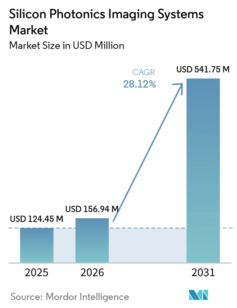
| Market Size (2026) | USD 156.94 Million |
| Market Size (2031) | USD 541.75 Million |
| Growth Rate (2026 - 2031) | 28.12 % |
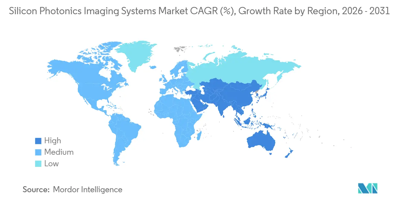
| Fastest Growing Market | Asia-Pacific |
| Largest Market | North America |
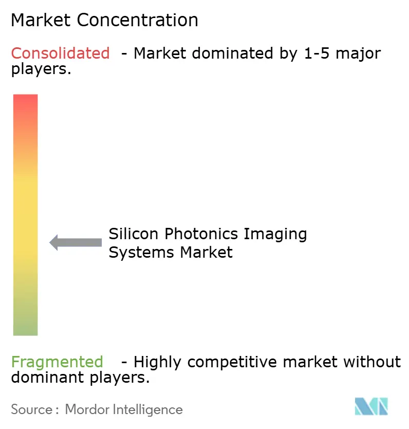
| Market Concentration | Medium |
Major Players *Disclaimer: Major Players sorted in no particular order Image © Mordor Intelligence. Reuse requires attribution under CC BY 4.0. | |
Silicon Photonics Imaging Systems Market Analysis by Mordor Intelligence
The silicon photonics imaging systems market size was valued at USD 124.45 million in 2025 and estimated to grow from USD 156.94 million in 2026 to reach USD 541.75 million by 2031, at a CAGR of 28.12% during the forecast period (2026-2031). Growth rests on manufacturing and design capabilities that are advancing through optical interconnect programs for artificial intelligence data centers. Those programs improve wafer capacity, photonic design tools, germanium photodetectors, silicon nitride waveguides, and wafer-level packaging that imaging developers can also use. This shared infrastructure can shorten imaging chip development cycles and lower the initial burden of advanced process development. Coherent detection is becoming a common technical base for LiDAR, optical coherence tomography, and holographic systems, which supports design reuse across applications. Packaging cost, test requirements, manufacturing yield, and access to intellectual property remain central constraints for the silicon photonics imaging systems market.
Key Report Takeaways
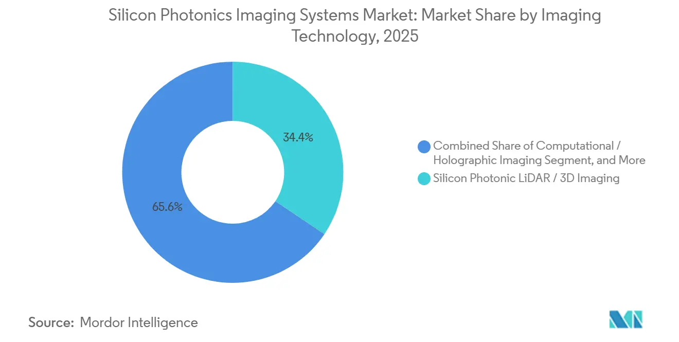
- By imaging technology, Silicon Photonic LiDAR and 3D Imaging accounted for 34.44% of the silicon photonics imaging systems market share in 2025, while Computational and Holographic Imaging is projected to expand at a 29.67% CAGR through 2031.
- By imaging modality, 3D Imaging accounted for 53.12% of revenue in 2025, while 3D Imaging is projected to expand at a 30.16% CAGR through 2031.
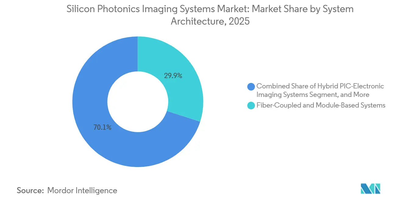
- By system architecture, Fiber-Coupled and Module-Based Systems held 29.91% of revenue in 2025, while Photonic Chiplet and Optical-Engine Systems are projected to expand at a 29.56% CAGR through 2031.
- By application, LiDAR and 3D Sensing held 32.21% of revenue in 2025, while Automotive is projected to expand at a 30.33% CAGR through 2031.
- By geography, North America held 38.81% of the silicon photonics imaging systems market in 2025, while Asia-Pacific is projected to expand at a 30.59% CAGR through 2031.
Note: Market size and forecast figures in this report are generated using Mordor Intelligence’s proprietary estimation framework, updated with the latest available data and insights as of January 2026.
Global Silicon Photonics Imaging Systems Market Trends and Insights
Drivers Impact Analysis*
| Driver | (~) % Impact on CAGR Forecast | Geographic Relevance | Impact Timeline |
|---|---|---|---|
| Solid-State FMCW LiDAR Adoption in Advanced Driver Assistance Systems | +6.5% | Global, led by Asia-Pacific and North America | Medium term (2-4 years) |
| AI and High-Performance Computing Photonic Interconnect Spillover | +5.8% | Global, concentrated in North America and Asia-Pacific | Short term (≤ 2 years) |
| Demand for Compact Optical Coherence Tomography and Point-of-Care Diagnostics | +4% | North America, Europe, Asia-Pacific | Medium term (2-4 years) |
| Miniaturization of Hyperspectral and Spectral Imaging Instruments | +3.2% | North America, Europe, Asia-Pacific | Long term (≥ 4 years) |
| Self-Imaging and Distributed Retinal Monitoring Deployment Models | +2.5% | North America and Europe | Long term (≥ 4 years) |
| Reusable Photonic Packaging Across Imaging and Sensing Platforms | +1.5% | Global | Medium term (2-4 years) |
| Source: Mordor Intelligence | |||
Solid-State FMCW LiDAR Adoption in Advanced Driver Assistance Systems
The silicon photonics imaging systems market benefits from the shift from time-of-flight detection to frequency-modulated continuous-wave LiDAR, which establishes a clear technical role for silicon photonics. Coherent FMCW detection reduces ambient-light interference and captures range and velocity from the optical signal. A 2025 study reported integrated photonic FMCW LiDAR measurement ranges up to 300 m, centimeter-scale resolution, and angular precision below 0.1 degrees. The same work identified automotive requirements, including velocity measurement up to 140 km/h at 200 m and 30 Hz refresh rates. Scantinel Photonics reported a 20 dB per-pixel signal-to-noise improvement and a tenfold reduction in LiDAR power use for its CMOS-based scanner-detector chip in 2024. A 2025 silicon photonic ranging engine also demonstrated 200 m operation with multi-channel signal amplification suited to automotive LiDAR packaging requirements.
AI and High-Performance Computing Photonic Interconnect Spillover
The silicon photonics imaging systems market benefits as artificial intelligence data-center investment is improving silicon photonics processes that imaging system developers can use. Ayar Labs raised USD 500 million in March 2026 to expand high-volume production and test capacity for co-packaged optical engine chiplets. The program focuses on active alignment, wafer-level test automation, and germanium-on-silicon photodetector yield. These are the same building blocks used in many coherent imaging systems. Nature Electronics noted that co-packaged optics and imaging platforms share modulators, balanced photoreceivers, and wavelength multiplexers. Tower Semiconductor reported more than USD 200 million in silicon photonics revenue in 2025 and stated that it is targeting further growth in 2026, adding scale to the manufacturing base available to the silicon photonics imaging systems market.
Demand for Compact Optical Coherence Tomography and Point-of-Care Diagnostics
The silicon photonics imaging systems market benefits as optical coherence tomography is moving beyond large hospital systems toward compact diagnostic equipment. Conventional systems have been priced from USD 50,000 to more than USD 200,000, which has limited access in community settings. Siloton captured a sub-surface retinal image using a photonic chip in June 2026, showing that chip-based OCT can produce clinically relevant imaging outside a laboratory setting. Its Akepa chip that combines more than 300 optical and electronic components in a package smaller than a quarter. The platform targets monitoring for wet AMD, diabetic macular edema, and retinal vein occlusion. A Horizon Europe project also reported a silicon nitride sensing platform for OCT, flow cytometry, and fluorescence sensing, achieving coupling efficiency up to 93%.
Reusable Photonic Packaging Across Imaging and Sensing Platforms
The silicon photonics imaging systems market could benefit as reusable packaging approaches could reduce repeated alignment work across imaging and sensing product lines. The main opportunity lies in standardizing fiber coupling, optical interfaces, and test methods across related photonic assemblies. The IEEE roadmap identifies photonic packaging as a major portion of the total cost of PIC-based products. It also reports that active fiber-to-chip alignment can take 30 to 60 seconds per fiber in existing production flows. Common packaging architectures would allow a larger volume base to support tooling and process development. This need is relevant to the silicon photonics imaging systems market because system costs remain closely tied to packaging yield and assembly time.
Restraints Impact Analysis*
| Restraint | (~) % Impact on CAGR Forecast | Geographic Relevance | Impact Timeline |
|---|---|---|---|
| High Cost of Photonic Packaging and Specialized Test Equipment | -2.8% | Global | Short term (≤ 2 years) |
| Low Yield and Limited Volume Manufacturing for Heterogeneous Integration | -1.8% | Global, concentrated in North America and Asia-Pacific | Medium term (2-4 years) |
| Clinical and Regulatory Validation of Chip-Based Imaging Architectures | -1.5% | North America and Europe | Long term (≥ 4 years) |
| Wavelength-Specific Calibration and Thermal Drift in Field Systems | -1.2% | Global | Long term (≥ 4 years) |
| Source: Mordor Intelligence | |||
High Cost of Photonic Packaging and Specialized Test Equipment
The silicon photonics imaging systems market faces a constraint due to persistent packaging costs. Electronic packaging uses passive placement, while fiber-to-chip coupling requires active alignment at sub-micron precision. The IEEE Heterogeneous Integration Roadmap reported alignment times of 30 to 60 seconds per fiber. It also identified PIC packaging costs as significantly higher than those of conventional electronic packaging.[1]IEEE Electronics Packaging Society, “Heterogeneous Integration Roadmap, Chapter 9, Photonics, 2025 Edition,” IEEE Heterogeneous Integration Roadmap, ieee.org. Imaging chips need optical tests for phase coherence, waveguide insertion loss, and photodetector responsivity, which increases equipment needs and test time. Emerging specifications from IEEE and the Integrated Photonic Systems Roadmap-International can guide coupling loss and alignment tolerance, but imaging-specific commercial certification is not yet established.
Low Yield and Limited Volume Manufacturing for Heterogeneous Integration
The silicon photonics imaging systems market faces a manufacturing constraint due to the heterogeneous integration of silicon waveguides with materials such as III-V gain media, thin-film lithium niobate, and germanium photodetectors. The combination broadens wavelength coverage and can improve coherence sensitivity, but each bonding interface can reduce yield. A May 2026 research paper reported micro-transfer printing yield above 95% and 3-sigma alignment accuracy below 500 nm on a 200 mm silicon photonics platform. The result remains at a research and low-volume production stage. A 2025 review found that adding non-silicon material layers compounds yield losses across the process stack. The IEEE roadmap also identified wafer bonding defects and wafer thinning as sources of photodetector reliability challenges.
*Our forecasts treat driver/restraint impacts as directional, not additive. The impact forecasts reflect baseline growth, mix effects, and variable interactions.
Segment Analysis
By Imaging Technology: Coherent Modalities Shape the Technology Mix
Silicon Photonic LiDAR and 3D Imaging accounted for 34.44% of imaging technology revenue in 2025, the largest share in the silicon photonics imaging systems market. Its role reflects its use in coherent FMCW detection for autonomous vehicles, robotic inspection, and perimeter security. Computational and Holographic Imaging is projected to expand at a 29.67% CAGR through 2031. A 2025 Nature Communications study demonstrated neural-operator computer-generated holography with 4K synthesis in 0.16 seconds per frame across a 30 mm depth range. Integrated metasurfaces can shape and focus light above silicon photonic circuits, reducing the need for external beam-shaping assemblies. These capabilities support compact coherent systems for augmented reality, scientific imaging, and security sensing.
Within the silicon photonics imaging systems market, optical coherence tomography and interferometric imaging form the second-largest technology cluster in the supplied analysis. Biomedical adoption is supported by the move toward chip-based systems, including Siloton's June 2026 retinal imaging milestone. Spectral and hyperspectral imaging is gaining use in pharmaceutical in-line analysis and food safety monitoring. Chip-scale spectrometers with sub-2 nm resolution can support embedded deployments that larger scanning cameras cannot address. Other imaging technologies include dual-comb spectroscopy and quantum photonic sensing for scientific metrology and defense work. Across the technology mix, coherent detection provides sensitivity and ambient-light rejection that direct-detection systems cannot provide at equivalent chip complexity.



By Imaging Modality: 3D Imaging Leads the Modality Mix
3D Imaging accounted for 53.12% of modality revenue in 2025, giving it the leading share in the silicon photonics imaging systems market, and is expected to grow with a CAGR of 30.16% over the forecast period. Depth sensing benefits from low phase noise, wavelength control, and the integration density of photonic integrated circuits. Conventional CMOS image sensors can serve many 2D intensity imaging applications at a lower cost. A 2026 Nature paper described a large-scale coherent 4D sensor with optical phased-array emitters and coherent focal-plane receivers. The platform mapped depth in real time and measured velocity for each pixel.[2]Nature Publishing Group, “A Large-Scale Coherent 4D Imaging Sensor,” Nature, nature.com. FMCW LiDAR production and adoption in augmented reality and surgical robotics can further support demand for 3D imaging through 2031.
Within the silicon photonics imaging systems market, 2D Imaging remains relevant for consumer spectroscopic sensors, industrial barcode readers, and laboratory scientific cameras. Its share is expected to decline as the cost of 3D capability falls. Other modalities include 4D imaging, polarimetric imaging, and multispectral imaging. These modes are strategically important in defense sensing, climate monitoring, and biomedical diagnostics because they capture multiple forms of information. A CLEO 2025 demonstration achieved 16.23 µm axial resolution with a silicon-based swept-source OCT system and a silica auxiliary interferometer.
By System Architecture: Module Systems Lead While Chiplets Advance
Fiber-Coupled and Module-Based Systems held 29.91% of system architecture revenue in 2025. Their position reflects the control they provide over thermal management, wavelength calibration, and fiber coupling. Modular systems can offer more reliable field operation when ambient temperatures exceed on-chip stabilization limits. Across the silicon photonics imaging systems market, most deployed silicon photonic LiDAR and OCT systems therefore retain fiber coupling as a reliability and serviceability choice. A 2026 packaging study reported that standard single-mode fiber arrays use pitches of at least 127 µm. This limit restricts density to 8 fibers per millimeter and creates a constraint that chiplet designs seek to address.
Photonic Chiplet and Optical-Engine Systems are projected to expand at a 29.56% CAGR through 2031. This is the fastest growth rate among the architecture categories of the silicon photonics imaging systems market. The approach separates optimization of the photonic die from electronic signal processing. OpenLight and Tower Semiconductor expanded their PH18DA ecosystem in August 2026, allowing circuit design in Cadence tools for InP-on-silicon platforms. Fully Integrated Photonic Imagers remain suitable for high-margin defense and scientific uses where yield losses can be absorbed. Hybrid PIC-electronic systems and free-space photonic-MEMS systems occupy other positions across current OCT, hyperspectral, scientific, and defense applications.
By Application: LiDAR Leads and Automotive Grows Fastest
LiDAR and 3D Sensing held 32.21% of application revenue in 2025. Coherent LiDAR uses phase-sensitive circuits, low-noise balanced photodetectors, and wavelength control that silicon photonics can integrate. Biomedical and Life Sciences is the second-largest application group in the supplied analysis. It includes ophthalmic and cardiac OCT, flow cytometry, and emerging diagnostic imaging systems. Industrial Inspection and Metrology uses photonic OCT and hyperspectral modules for non-contact surface measurement and tablet coating verification. These users value spatial coherence and measurement traceability in accordance with the requirements of ISO/IEC 17025.
The automotive sector is projected to expand at a 30.33% CAGR through 2031. Euro NCAP 2025 protocols and US automated emergency braking performance standards support demand for stronger driver-assistance capabilities. FMCW LiDAR can support 300 m detection, centimeter-level resolution, velocity extraction, and 30 Hz operation. Consumer electronics drive demand through biometric recognition and augmented-reality depth sensing. Aerospace and defense applications include optical aperture synthesis and spectral intelligence. Scientific research, environmental monitoring, agricultural remote sensing, and mine safety further expand the addressable market for silicon photonics imaging systems.
Geography Analysis
North America accounted for 38.81% of global revenue in 2025, the leading share of the silicon photonics imaging systems market by geography. The region combines artificial intelligence hardware companies, photonic foundries, and defense procurement for sensing systems. Four of five global companies with confirmed co-packaged optics revenue by mid-2026 were US-based, according to the supplied analysis. NVIDIA's March 2026 agreements with Lumentum and Coherent included USD 2 billion investments in each company.
The silicon photonics imaging systems market in Europe is building a regional base through public-private investment and established strengths in medical photonics and automotive sensing research. PhotonixFAB is developing a European supply chain for SOI- and silicon nitride photonics with heterogeneous integration capabilities. The STMicroelectronics-led STARLight project is intended to establish a high-volume 300 mm silicon photonics line by 2028. The United Kingdom contributes through Siloton's chip-based OCT work, while France supports imaging-grade PIC development through CEA-Leti and the PIXEurope pilot line.
Asia-Pacific is projected to expand at a 30.59% CAGR through 2031, the fastest regional rate in the silicon photonics imaging systems market. Japan is central to this expansion through manufacturing investment and photonics policy. Tower Semiconductor announced a Japan expansion in July 2026 with USD 3 billion in investment net of grants and USD 1 billion in METI grants.[3]Tower Semiconductor, “Tower Semiconductor with METI Support Announces Strategic Capacity Expansion in Japan,” Tower Semiconductor Press Release, towersemi.com. The plan targets 300 mm silicon photonics, silicon germanium, and advanced optical packaging capacity, with track-one production readiness targeted for Q4 2027.

Competitive Landscape
The silicon photonics imaging systems market is moderately fragmented at the end-product layer, while the foundry layer is becoming more concentrated. GlobalFoundries acquired Advanced Micro Foundry in Singapore in November 2025. The acquisition added manufacturing assets, intellectual property, and more than 15 years of silicon photonics manufacturing experience to its Fotonix platform. Tower Semiconductor reported silicon photonics revenue above USD 200 million in 2025. It also reported USD 1.3 billion in customer contracts for 2027 revenue and USD 290 million in capacity-reservation prepayments.
Imaging specialists compete through coherent performance and application-specific product design rather than price alone. SiLC Technologies has filed a 2026 US patent application covering an expanded imaging range for FMCW LiDAR for driver-assistance and augmented-reality applications. Siloton uses an intellectual-property-protected chip-based OCT platform and is pursuing a regulatory pathway for its handheld ophthalmic system. The company demonstrated commercial PIC-based retinal imaging in a human subject in June 2026. These moves show that validation, packaging capability, and defensible system design affect competitive positioning as much as photonic chip performance.
For the silicon photonics imaging systems market, foundry choices shape product road maps because imaging companies must design around each platform's process rules and yield profile. Intellectual-property concentration among established semiconductor and communications companies creates freedom-to-operate risks for smaller developers. Wafer-level test automation remains an opportunity for suppliers to shorten characterization time for imaging PICs. Reusable photonic packaging can reduce repeated fiber-alignment costs across product lines.
Silicon Photonics Imaging Systems Industry Leaders
Intel Corporation
Hamamatsu Photonics K.K.
Lumentum Holdings Inc.
Coherent Corp.
SiLC Technologies, Inc.
- *Disclaimer: Major Players sorted in no particular order

Recent Industry Developments
- August 2026: Lightmatter, Inc. formally launched the Open Silicon Photonics for AI Systems initiative as an official workstream within the Open Compute Project, releasing a 300-page Architecture Vision white paper alongside 19 founding member companies, including Celestica, Dell Technologies, Flex, Foxconn Interconnect Technology, Qualcomm, and Quanta Cloud Technology.
- August 2026: OpenLight and Tower Semiconductor announced the availability of OpenLight's photonic process design kit within Cadence electronic design automation tools for Tower's PH18DA InP-on-silicon photonics platform. The integration enables imaging-focused PIC designers to develop advanced circuits for 400G and 1.6T applications within industry-standard IC design environments, removing the EDA toolchain barrier that had required specialized photonic-specific design flows.
- July 2026: Tower Semiconductor announced a dual-track capacity expansion in Japan, committing USD 3 billion net of grants with Japan's Ministry of Economy, Trade and Industry providing USD 1 billion in government subsidies. The expansion targets 300 mm silicon photonics and silicon germanium capacity at repurposed facilities in Toyama and Niigata prefectures, with Q4 2027 targeted for full production readiness on track one, materially increasing global supply of imaging-grade silicon photonics wafers ahead of forecast demand.
- June 2026: Siloton Limited captured the first sub-surface retinal image using its Akepa photonic chip-based OCT system, establishing the first commercial demonstration of PIC-based retinal imaging in a human subject. The company is pursuing FDA clearance and CE marking for a handheld ophthalmic OCT device targeting wet AMD, diabetic macular edema, and other retinal disease monitoring.


Global Silicon Photonics Imaging Systems Market Report Scope
The Silicon Photonics Imaging Systems Market encompasses imaging solutions that use silicon photonics technology to transmit, process, and detect optical signals on silicon-based integrated circuits. These systems support high-speed, high-resolution imaging applications across healthcare, industrial inspection, consumer electronics, and scientific research by enabling compact designs, lower power consumption, and enhanced data transmission capabilities.
The Silicon Photonics Imaging Systems Market Report is Segmented by Imaging Technology (Silicon Photonic LiDAR and 3D Imaging, OCT, Interferometric Imaging, Computational and Holographic Imaging, Spectral and Hyperspectral Imaging, and Other Imaging Technologies), Imaging Modality (2D Imaging, 3D Imaging, and Other Imaging Modalities), System Architecture (Fully Integrated Photonic Imagers, Photonic Chiplet and Optical-Engine Systems, Hybrid PIC-Electronic Imaging Systems, Fiber-Coupled and Module-Based Systems, and Free-Space and Photonic-MEMS Hybrid Systems), Application (LiDAR and 3D Sensing, Biomedical and Life Sciences, Industrial Inspection and Metrology, Consumer Electronics, Automotive, Aerospace and Defense, Scientific and Research, and Other Applications), and Geography (North America, South America, Europe, Asia-Pacific, Middle East, and Africa). The Market Forecasts are Provided in Terms of Value (USD).
| Silicon Photonic LiDAR / 3D Imaging |
| OCT |
| Interferometric Imaging |
| Computational / Holographic Imaging |
| Spectral / Hyperspectral Imaging |
| Other Imaging Technologies |
| 2D Imaging |
| 3D Imaging |
| Other Imaging Modalities |
| Fully Integrated Photonic Imagers |
| Photonic Chiplet and Optical-Engine Systems |
| Hybrid PIC-Electronic Imaging Systems |
| Fiber-Coupled and Module-Based Systems |
| Free-Space and Photonic-MEMS Hybrid Systems |
| LiDAR and 3D Sensing |
| Biomedical and Life Sciences |
| Industrial Inspection and Metrology |
| Consumer Electronics |
| Automotive |
| Aerospace and Defense |
| Scientific and Research |
| Other Applications |
| North America | United States |
| Canada | |
| Mexico | |
| South America | Brazil |
| Argentina | |
| Chile | |
| Rest of South America | |
| Europe | Germany |
| United Kingdom | |
| France | |
| Italy | |
| Spain | |
| Rest of Europe | |
| Asia-Pacific | China |
| Japan | |
| India | |
| South Korea | |
| Australia | |
| Rest of Asia-Pacific | |
| Middle East | United Arab Emirates |
| Saudi Arabia | |
| Qatar | |
| Rest of Middle East | |
| Africa | South Africa |
| Egypt | |
| Nigeria | |
| Rest of Africa |
| By Imaging Technology | Silicon Photonic LiDAR / 3D Imaging | |
| OCT | ||
| Interferometric Imaging | ||
| Computational / Holographic Imaging | ||
| Spectral / Hyperspectral Imaging | ||
| Other Imaging Technologies | ||
| By Imaging Modality | 2D Imaging | |
| 3D Imaging | ||
| Other Imaging Modalities | ||
| By System Architecture | Fully Integrated Photonic Imagers | |
| Photonic Chiplet and Optical-Engine Systems | ||
| Hybrid PIC-Electronic Imaging Systems | ||
| Fiber-Coupled and Module-Based Systems | ||
| Free-Space and Photonic-MEMS Hybrid Systems | ||
| By Application | LiDAR and 3D Sensing | |
| Biomedical and Life Sciences | ||
| Industrial Inspection and Metrology | ||
| Consumer Electronics | ||
| Automotive | ||
| Aerospace and Defense | ||
| Scientific and Research | ||
| Other Applications | ||
| By Geography | North America | United States |
| Canada | ||
| Mexico | ||
| South America | Brazil | |
| Argentina | ||
| Chile | ||
| Rest of South America | ||
| Europe | Germany | |
| United Kingdom | ||
| France | ||
| Italy | ||
| Spain | ||
| Rest of Europe | ||
| Asia-Pacific | China | |
| Japan | ||
| India | ||
| South Korea | ||
| Australia | ||
| Rest of Asia-Pacific | ||
| Middle East | United Arab Emirates | |
| Saudi Arabia | ||
| Qatar | ||
| Rest of Middle East | ||
| Africa | South Africa | |
| Egypt | ||
| Nigeria | ||
| Rest of Africa | ||


Key Questions Answered in the Report
What is the silicon photonics imaging systems market size?
The silicon photonics imaging systems market size is estimated at USD 156.94 million in 2026 and is forecast to reach USD 541.75 million by 2031, at a 28.12% CAGR.
What is driving demand for silicon photonics imaging systems?
Demand is supported by FMCW LiDAR adoption, artificial intelligence optical-interconnect manufacturing spillover, compact OCT, and miniaturized spectral imaging.
Which imaging technology held the largest share in 2025?
Silicon Photonic LiDAR and 3D Imaging held 34.44% of imaging technology revenue in 2025.
Which application is expected to grow fastest through 2031?
Automotive is projected to expand at a 30.33% CAGR through 2031, supported by advanced driver-assistance requirements and FMCW LiDAR adoption.
Which region is expected to grow fastest through 2031?
Asia-Pacific is projected to expand at a 30.59% CAGR through 2031, supported by manufacturing investment in Japan, China, and South Korea.
What is the key cost challenge for silicon photonic imaging systems?
Photonic packaging and specialized optical test equipment remain major cost challenges because fiber-to-chip alignment requires sub-micron precision.
Page last updated on: