
Silicon Carbide Power Semiconductor Market Size and Share
Market Overview
| Study Period | 2020 - 2031 |
|---|---|
| Market Size (2026) | USD 3.41 Billion |
| Market Size (2031) | USD 10.26 Billion |
| Growth Rate (2026 - 2031) | 24.68 % |
| Fastest Growing Market | North America |
| Largest Market | Asia Pacific |
| Market Concentration | Medium |
Major Players *Disclaimer: Major Players sorted in no particular order Image © Mordor Intelligence. Reuse requires attribution under CC BY 4.0. | |
Silicon Carbide Power Semiconductor Market Analysis by Mordor Intelligence
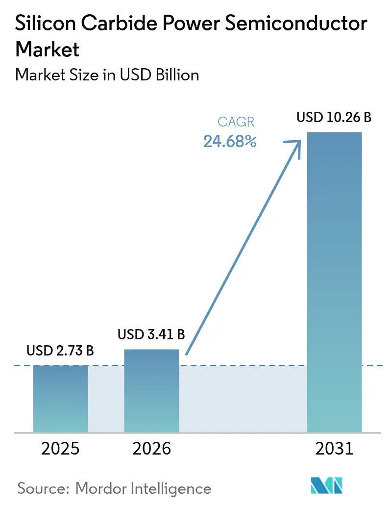
Silicon carbide power semiconductor market size in 2026 is estimated at USD 3.41 billion, growing from 2025 value of USD 2.73 billion with 2031 projections showing USD 10.26 billion, growing at 24.68% CAGR over 2026-2031. The growth curve is propelled by the technology’s wide-bandgap advantages—higher breakdown voltage, lower switching losses, and superior thermal conductivity—that unlock performance envelopes unattainable with legacy silicon devices. Mandated electrification targets, fast-charging rollouts above 350 kW, and policy-backed capacity additions in 150 mm and 200 mm fabs converge to strengthen demand visibility. Supply–demand dynamics are further shaped by vertical integration moves among automotive OEMs, aggressive wafer-size transitions to 8-inch, and geopolitical incentives such as the US CHIPS Act and EU IPCEI funding that redirect capital toward onshore manufacturing. Although defect densities and package-level thermal limits remain cost headwinds, volume ramps across EV traction inverters, data-center power shelves, and high-voltage renewables keep the Silicon carbide power semiconductor market on a steep adoption trajectory.[1]European Commission, “Regulation (EU) 2019/631 setting CO₂ emission performance standards,” europa.eu
Key Report Takeaways
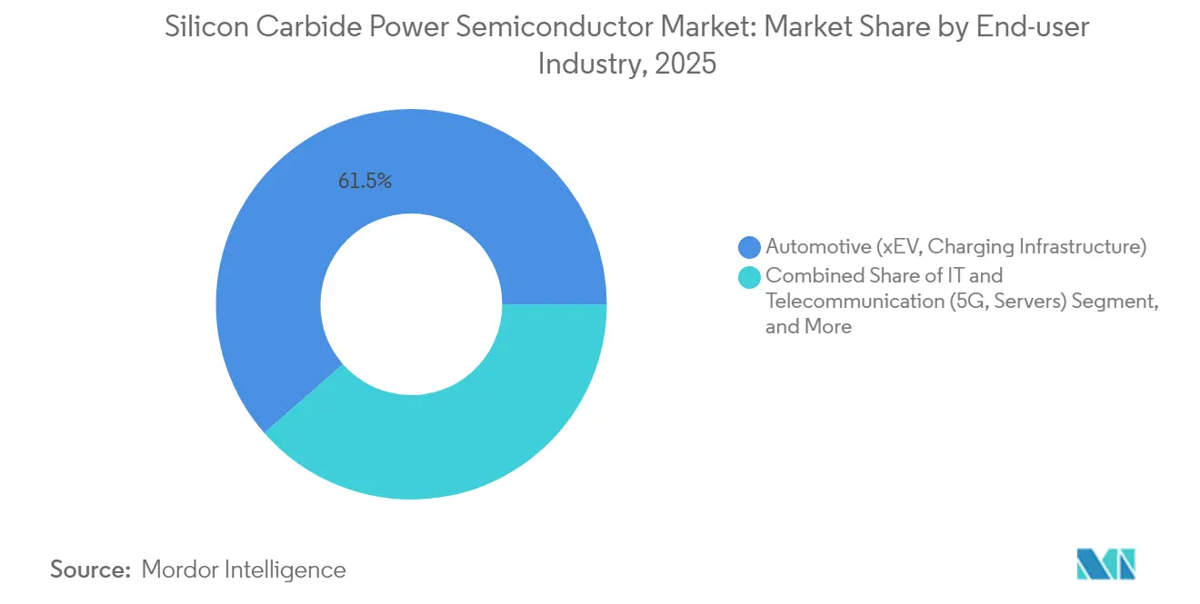
- By end-user industry, automotive commanded a 61.45% share of the Silicon carbide power semiconductor market in 2025, while fast-charging infrastructure is projected to surge at a 26.25% CAGR to 2031.
- By device type, discrete MOSFETs held 43.35% revenue share in 2025; power modules are forecast to grow at a 10.05% CAGR through 2031.
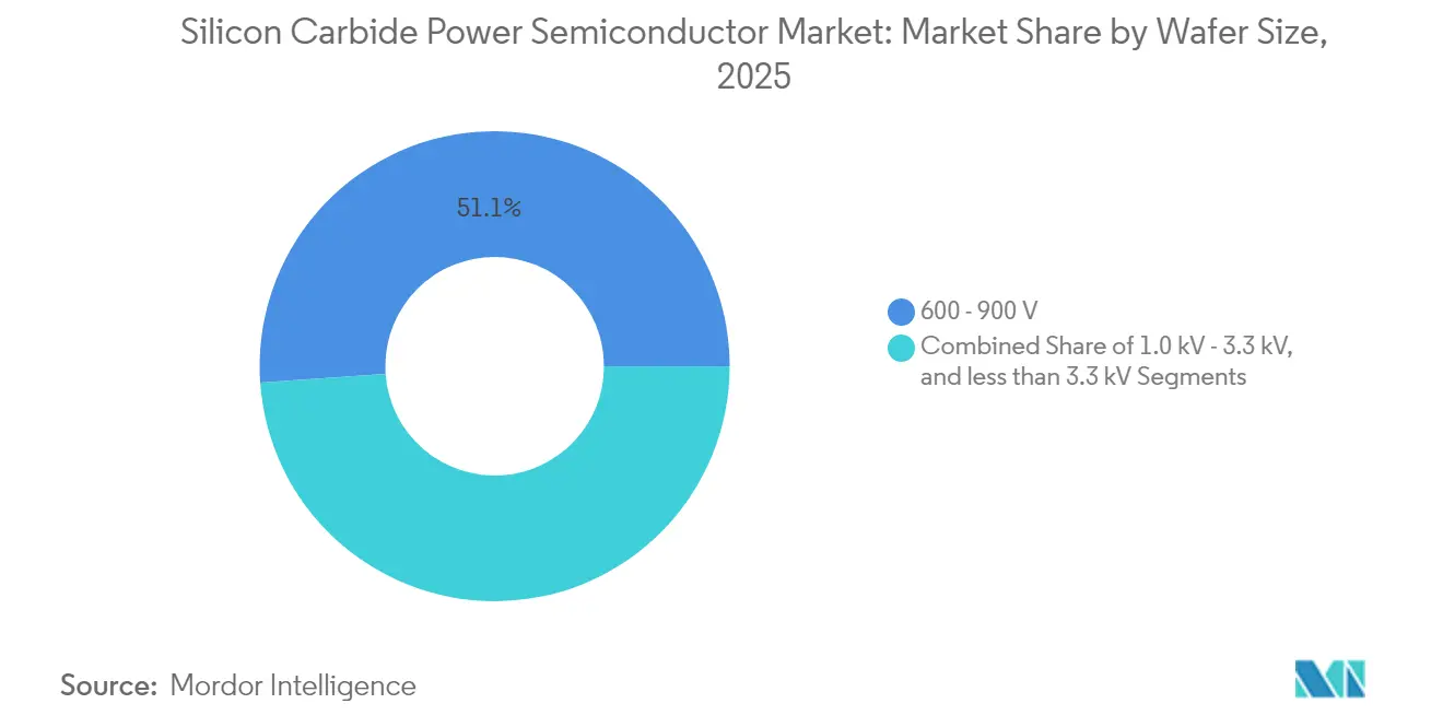
- By voltage rating, the 600-900 V band led with 51.12% share in 2025; the >3.3 kV class is expected to advance at 9.64% CAGR to 2031.
- By wafer size, 6-inch substrates accounted for 72.35% of the Silicon carbide power semiconductor market share in 2025, whereas 200 mm wafers are expanding at a 9.31% CAGR.
- By packaging technology, wire-bonded solutions dominated with 64.25% share in 2025; sintered packages are forecast to post a 10.18% CAGR through 2031.
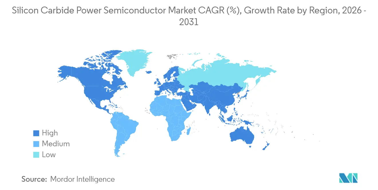
- By geography, Asia-Pacific led with 55.92% share in 2025; North America exhibits the fastest regional CAGR at 27.35% through 2031.
- Infineon Technologies, STMicroelectronics, Wolfspeed, Onsemi, and ROHM jointly controlled over 90% of global revenue in 2024, underscoring a highly concentrated supply base.
Note: Market size and forecast figures in this report are generated using Mordor Intelligence’s proprietary estimation framework, updated with the latest available data and insights as of 2026.
Market Trends and Insights
Drivers Impact Analysis of Silicon Carbide Power Semiconductor Market*
| Driver | (~) % Impact on CAGR Forecast | Geographic Relevance | Impact Timeline |
|---|---|---|---|
| EV traction-inverter efficiency mandates | +8.50% | Global, with early adoption in EU and China | Medium term (2-4 years) |
| Global SiC-fab capacity expansions (150- and 200 mm) | +6.20% | APAC core, spill-over to North America and EU | Long term (≥ 4 years) |
| Wide-bandgap policy incentives (US CHIPS, EU IPCEI) | +4.80% | North America and EU | Medium term (2-4 years) |
| High-voltage fast-charging roll-out (>350 kW) | +7.10% | Global, with concentration in developed markets | Short term (≤ 2 years) |
| OEM vertical integration to secure wafers | +3.90% | Global, led by automotive OEMs | Medium term (2-4 years) |
| Under-the-radar: SiC adoption in data-center power shelves | +5.30% | North America and Asia-Pacific | Short term (≤ 2 years) |
| Source: Mordor Intelligence | |||
EV Traction-Inverter Efficiency Mandates
Regulatory pressure in Europe and China compels automakers to squeeze every percentage of drivetrain efficiency. SiC MOSFET-based 800 V architectures deliver 2-4% energy savings relative to silicon IGBT solutions, translating to lighter battery packs or extended range. The European Commission’s 2025-2030 fleet CO₂ limits elevate SiC from niche to mainstream, while BYD’s megawatt-class flash-charging prototype highlights how lower switching losses curb station-level CAPEX. Tesla’s long-term wafer sourcing agreements exemplify how OEMs treat SiC access as strategic, reinforcing volume-driven cost erosion that benefits the broader Silicon carbide power semiconductor market.[2]BYD Company Limited, “Megawatt Charging Solution Press Release,” byd.com
Global SiC-Fab Capacity Expansions (150 and 200 mm)
Transitions from 150 mm to 200 mm wafers multiply die output per run by roughly 2.2× while cutting unit costs up to 40%. Wolfspeed’s Mohawk Valley fab in New York and Infineon’s Kulim 2 line in Malaysia exemplify the USD-billion-scale investments required, reinforcing high entry barriers. Taiwan’s National Applied Research Laboratories recently demonstrated nanosecond-laser grinding that halves wafer breakage, accelerating 8-inch adoption. As capital flows concentrate in APAC, Western funding programs aim to de-risk regional dependence.
Wide-Bandgap Policy Incentives (US CHIPS, EU IPCEI)
The US CHIPS Act earmarks subsidies for domestic SiC substrate and epitaxy lines, while Europe’s IPCEI framework aggregates multinational grants for end-to-end wide-bandgap value chains. These schemes synchronize with the industry’s shift toward 8-inch, enabling late-stage entrants to leapfrog older tooling. However, effectiveness rests on mobilizing private capex and workforce skill sets that remain clustered in Asia.
High-Voltage Fast-Charging Roll-Out (>350 kW)
Operators moving to 400–500 kW dispensers discover that SiC cuts converter footprints and cooling loads, trimming both CAPEX and OPEX. Shinry Technologies’ partnership with Wolfspeed on 500 kW modules underscores rising cross-border collaborations. Because station utilization scales with dwell time, every 1% efficiency gain magnifies return on investment, catalysing SiC pull-through across rectification and power-sharing stages.
Restraints Impact Analysis of Silicon Carbide Power Semiconductor Market*
| Restraint | (~) % Impact on CAGR Forecast | Geographic Relevance | Impact Timeline |
|---|---|---|---|
| SiC wafer defect density and cost premium | -4.20% | Global, particularly affecting cost-sensitive applications | Medium term (2-4 years) |
| Packaging thermal-cycle reliability limits | -2.80% | Global, with higher impact in harsh environment applications | Long term (≥ 4 years) |
| Downtime risk from hydrogen-etch furnaces | -1.90% | Manufacturing centers in APAC and North America | Short term (≤ 2 years) |
| Under-the-radar: FZ-grown GaN competing in 650 V nodes | -3.10% | Applications requiring 650V operation, primarily in APAC | Medium term (2-4 years) |
| Source: Mordor Intelligence | |||
SiC Wafer Defect Density and Cost Premium
Threading dislocations and basal-plane defects remain 5–10× above mature silicon benchmarks, depressing yields and elevating die costs by 3–5×. While crystal-growth refinements are closing the gap, the interim premium delays adoption in price-sensitive inverters. Process-learning curves tied to 200 mm migrations may briefly widen cost deltas before improved throughputs guide the Silicon carbide power semiconductor market back toward silicon-plus parity.[3]ROHM Semiconductor, “High-Density SiC Module Datasheet,” rohm.com
Packaging Thermal-Cycle Reliability Limits
Coefficient-of-expansion mismatches between SiC dies and Al wire bonds trigger fatigue under rapid load swings, especially in 150 °C ambient environments. ROHM’s HSDIP20 4-in-1 and 6-in-1 modules adopt sintered silver and uniform pressure designs to triple power density, yet qualification protocols remain lengthier than for legacy packages. Automotive and aerospace platforms with extended mission lifetimes keep reliability scrutiny high.
*Our forecasts treat driver/restraint impacts as directional, not additive. The impact forecasts reflect baseline growth, mix effects, and variable interactions.
Silicon Carbide Power Semiconductor Market Segment Analysis
By End-User Industry:
Automotive Drives Market LeadershipThe automotive segment generated 61.45% of 2025 revenue, underscoring its pivotal role in scaling the Silicon carbide power semiconductor market. EV makers migrating to 800 V systems specify SiC as default to meet efficiency and charging objectives. Fast-charging infrastructure, despite a smaller 2024 base, is the fastest-growing subsegment at 26.25% CAGR to 2031 as networks move to >350 kW dispensers. Rising interest from data-center operators positions IT and telecom as the second-largest buyer pool, with server power shelves using SiC to pare conversion losses. Renewable power converters and industrial motion drives adopt SiC for frequency-switching gains that shrink magnetics, while rail and e-aviation platforms explore high-temperature resilience. Onsemi’s USD 115 million JFET buy signals strategic bets on AI and cloud workloads that could diversify revenue streams beyond traction over the forecast window.
SiC’s value proposition in mobility stands on quantifiable lifetime savings. Adoption enables smaller battery packs, shorter installation downtimes, and fewer cooling loops, creating a positive feedback loop that widens the Silicon carbide power semiconductor market addressable base. Government credits tied to efficiency thresholds further sharpen OEM focus. Concurrently, tier-one suppliers bundle SiC inverter control boards with advanced gate drivers to accelerate platform-level time-to-market, reinforcing ecosystem lock-in.



By Device Type:
Discrete MOSFETs Lead, Modules AccelerateDiscrete MOSFETs and JFETs held 43.35% share in 2025, favoured by engineers prioritizing design flexibility and cost optimization. Yet power modules, growing at 10.05% CAGR, increasingly displace discrete as integrators transition toward single-package solutions that streamline thermal paths and shorten qualification cycles. Schottky diodes fill complementary roles in synchronous rectification, often paired within module footprints to minimize parasitic.
The Silicon carbide power semiconductor market size for power modules is projected to expand quickly as vertical integration strategy aligns with OEM production ramps. Moulded and press-fit module roadmaps promise tighter RDS (on) uniformity, while integrated current-sense functions simplify control loops. Bare die and foundry service sales rise in tandem, serving specialized traction and renewable players that require custom layouts. Device suppliers leverage proprietary trench topologies and JFET cascades to push efficiency limits, sustaining a cycle of incremental gains that justify SiC’s premium over silicon super junction MOSFETs.
By Voltage Rating:
600-900 V Dominates, High-Voltage AcceleratesThe 600-900 V class captured 51.12% share in 2025, the sweet spot for 800 V EV drivetrains and industrial drives. Designs at this voltage realize full SiC benefits—switching frequency headroom and reduced conduction losses—without prohibitive die costs. The >3.3 kV tier, forecast to grow at 9.64% CAGR, unlocks grid-level applications such as solar string inverters and battery energy storage where higher blocking capability shrinks transformer footprints.
The Silicon carbide power semiconductor market size for >3.3 kV devices is poised to climb as transmission grids adopt HVDC topologies to integrate intermittent renewables. Mid-voltage 1.0–3.3 kV products address locomotive propulsion and wind-turbine converters. Semikron Danfoss’ integration of ROHM’s 2 kV MOSFETs into SMA’s utility-scale plant signals wider acceptance of SiC in 1500 V DC-link designs. System designers increasingly weigh total installed cost—including reduced passive components—rather than device ASP when selecting voltage classes.
By Wafer Size:
6-Inch Leads, 8-Inch SurgesSix-inch substrates composed 72.35% of shipments in 2025, reflecting established crystal-pulling infrastructure. However, the 8-inch bracket is on a 9.31% CAGR trajectory, cementing itself as the cost-reduction lever that enables broader market penetration. Each 200 mm wafer yields more than double the die count of a 150 mm wafer, easing foundry amortization and accelerating volume learning.
Such scale economics re-shape the Silicon carbide power semiconductor market share hierarchy as capital-rich incumbents leap ahead. Taiwan’s laser-grinding breakthrough lowers kerf loss, pulling wafer-cost curves downward. Smaller firms remain on 4-inch lines for niche aerospace and medical roles, yet risk marginalization as OEM qualification cycles pivot to 200 mm supply assurances.
Geography Analysis
APAC Silicon Carbide Power Semiconductor Market
Asia-Pacific retained 55.92% of 2025 revenue, leveraging China’s EV dominance, Japan’s crystal-growth leadership, and South Korea’s module-assembly competence. Region-wide synergies shorten lead times and compress costs, reinforcing first-mover advantage for APAC champions even as export-control uncertainties loom. Home-grown substrate vendors such as TankeBlue reduce reliance on Western boule suppliers, enabling vertically integrated stacks that serve domestic auto OEMs.
North America Silicon Carbide Power Semiconductor Market
North America is projected to outpace all other regions with a 27.35% CAGR to 2031. CHIPS Act incentives, Wolfspeed’s Mohawk Valley wafer output, and automotive plant re-tooling’s in the US Midwest converge to lift local demand. Data-center operators adopting 800 V DC topologies provide an additional pull, while cross-border partnerships—Shinry and Wolfspeed on supercharger build-outs—demonstrate the openness of US firms to alliances that secure fast-ramp volumes.
EMEA and South America Silicon Carbide Power Semiconductor Market
Europe follows in market share, propelled by fleet-wide CO₂ targets and a robust renewable-energy pipeline. IPCEI funding has seeded projects such as the “SiC Valley” in Catania, anchoring substrate, epi, and device fabrication in a single locale. However, limited native boule capacity leaves the region dependent on imports, a gap policymakers aim to close through joint ventures with Japanese crystal-growth specialists. Emerging regions in the Middle East, Africa, and South America remain minor today but signal latent demand through large-scale solar tenders and e-bus fleet pilots that favour SiC’s high-temperature resilience.

Regulatory Landscape
Policy and standards are tightening around high-voltage (1200 V+) SiC devices, with certification increasingly treated as a market-entry requirement rather than a buyer preference. In the European Union, the EU Chips Act (Regulation (EU) 2023/1781) and the Strategic Technologies for Europe Platform (STEP, Regulation (EU) 2024/795) anchor the industrial-policy push toward resilient semiconductor supply chains. A July 2026 European Commission measure (EU/2026/1843) links market access for 1200 V+ SiC power devices to AEC-Q101:2026 Rev.2 certification and ISO/IEC 17025-accredited test reporting, which increases compliance costs for suppliers without established automotive-grade qualification pipelines.
In the United States, wide-bandgap incentives under the CHIPS and Science Act are complemented by compliance-focused actions affecting imports. A July 2026 interim final rule described in the market notes requires certified energy-efficiency compliance declarations and dual-standard verification (UL 62368-1 and AEC-Q101) for 1200 V+ SiC MOSFET imports. Japan is also using policy tools to steer trade flows, with METI introducing a May 2026 Green Semiconductor Materials Export Promotion White List tied to JIS C 7041-2:2025 energy-efficiency classification, which creates a differentiated pathway for pre-qualified, high-efficiency trench-gate SiC products.
Competitive Landscape
The Silicon carbide power semiconductor market is oligopolistic: the five largest suppliers held over 90% revenue in 2024. High capital intensity for 150 mm and 200 mm fabs, crystallization expertise, and decades-long patent portfolios erect formidable barriers. Incumbents follow vertical-integration playbooks that begin with boule growth, progress through epitaxy, and culminate in in-house module packaging, locking in quality and cost control.
Infineon, STMicroelectronics, and Wolfspeed expand 200 mm capacity ahead of demand curves, underpinning multiyear supply agreements with Tesla, Hyundai, and Lucid. Onsemi and ROHM differentiate via trench architectures and high-temperature gate oxides. Disruptors such as BYD Semiconductor press cost advantages in domestic markets through government-supported capex and captive EV demand. CRRC Times Electric leverages traction know-how to court rail customers seeking SiC retrofits. Patent database analytics reveal 13,700+ active families, underscoring a landscape where litigation risk coexists with co-development pacts that accelerate ecosystem maturation.
Geopolitics increasingly permeate strategy. US export controls on advanced toolsets encourage Chinese champions to build turnkey equipment ecosystems, while EU resilience policies favour regional sourcing, nudging global supply toward a multipolar configuration. Collective R and D spend tops USD 2 billion annually, concentrated on 200 mm wafer yield, ultralow RDS (on) cells, and sintered packaging that unlock >3 kV designs. Competitive positioning will hinge less on pure device pricing and more on co-optimized module, gate-driver, and thermal-stack solutions.
Silicon Carbide Power Semiconductor Industry Leaders
Infineon Technologies AG
STMicroelectronics N.V.
Wolfspeed Inc.
onsemi Corporation
ROHM Co., Ltd.
- *Disclaimer: Major Players sorted in no particular order

Silicon Carbide Power Semiconductor Market Companies Covered in this Report
- Infineon Technologies AG
- STMicroelectronics N.V.
- Wolfspeed Inc.
- onsemi Corporation
- ROHM Co., Ltd.
- Semikron Danfoss GmbH & Co. KG
- Mitsubishi Electric Corporation
- Fuji Electric Co., Ltd.
- Toshiba Electronic Devices & Storage Corporation
- Microchip Technology Inc.
- Qorvo SiC (United Silicon Carbide)
- GeneSiC Semiconductor Inc.
- Littelfuse Inc. (IXYS)
- Navitas Semiconductor Corp.
- Power Integrations Inc.
- Hitachi Energy Ltd.
- Global Power Technologies Group Inc.
- StarPower Semiconductor Ltd.
- BYD Semiconductor Co., Ltd.
- CRRC Times Electric Co., Ltd.
Read Analysis of Silicon Carbide Power Semiconductor Companies

Market Opportunities and Future Outlook
The clearest whitespace for suppliers and ecosystem partners is at the intersection of 200 mm manufacturing scale-up and qualification-ready product pipelines for automotive, charging, and emerging data-center power architectures. Public funding and industrial-policy programs are underwriting capacity and localization moves, including the US Department of Commerce CHIPS Program Office executing a USD 225 million direct funding agreement with Bosch in July 2026 to support a broader USD 2 billion SiC investment in Roseville, California, along with sample production that began in July 2026.
In Europe, the EU Chips Act framework supports multi-year build-outs such as STMicroelectronics' 200 mm SiC program in Catania, Italy (a EUR 5 billion multi-year investment program). Infineon also opened its Smart Power Fab in Dresden as a EUR 5 billion investment project to expand power semiconductor manufacturing capability. Commercial opportunities are expanding further around higher-voltage and higher-temperature device roadmaps, along with packaging and qualification services required to industrialize them at volume. Infineon's rollout of SiC products based on 200 mm wafer technology in Villach (initiated in Q1 2025) and onsemi's expanded Bucheon, South Korea SiC facility (built for full capacity above one million 200 mm SiC wafers annually) show where near-term supplier selection and second-sourcing decisions are concentrated. As EU and US market-entry requirements increasingly reference AEC-Q101 and ISO/IEC 17025 lab validation for 1200 V+ classes, additional demand is emerging for accredited test capacity, automotive-grade reliability engineering, and module-level thermal-cycle solutions (including sintered and top-side-cooled approaches) aimed at reducing qualification timelines for traction inverters, >350 kW charging power stages, and 800 V DC power shelves.
Recent Industry Developments in Silicon Carbide Power Semiconductor Market
- July 2026: Infineon Technologies started supplying silicon carbide technology to ADVANTICS for power converters used in megawatt charging systems. The move improves Infineon’s position in high-power charging architectures where efficiency and thermal design constrain station footprint and total cost of ownership.
- May 2026: Infineon Technologies launched a 1300 V silicon carbide module in its HybridPACK Drive family for electric vehicle inverters, with operation specified up to 205 C. This extends SiC module performance into higher-temperature operating envelopes that support higher power density and simplified cooling at the inverter level.
- September 2024: STMicroelectronics unveiled a new generation of silicon carbide power technology tailored for next-generation EV traction inverters. The announcement reinforced the industry shift toward platform-level SiC roadmaps for 800 V drivetrains, shaping long-cycle OEM and tier-one qualification decisions.


Silicon Carbide Power Semiconductor Market Report Scope and Research Methodology
Market Definition and Coverage
For this study, the silicon carbide power semiconductor market covers revenues from SiC-based power devices sold into power conversion and power control uses across automotive, industrial, energy, and IT infrastructure demand.
Scope exclusions: Excludes non-SiC power semiconductors (for example, silicon or gallium nitride devices) and adjacent passive components used around the power stage.
Segments Covered in This Report
- Segmentation by End-user Industry
- Automotive (xEV, Charging Infrastructure)
- IT and Telecommunication (5G, Servers)
- Power (PV, Wind, UPS, ESS)
- Industrial (Motor Drives, Robotics)
- Transportation - Rail and Aviation
- Other End-User (Oil and Gas, Medical, R&D)
- Segmentation by Device Type
- Discrete MOSFET / JFET
- Power Module
- Schottky Diode
- Bare Die / Foundry Service
- Segmentation by Voltage Rating
- 600 - 900 V
- 1.0 kV - 3.3 kV
- > 3.3 kV
- Segmentation by Wafer Size
- 4-inch
- 6-inch (150 mm)
- 8-inch (200 mm+)
- Segmentation by Packaging Technology
- Wire-Bonded
- Sintered
- Press-fit
- Flip-Chip / Embedded Die
- Segmentation by Geography
- North America
- United States
- Canada
- Mexico
- Europe
- United Kingdom
- Germany
- France
- Italy
- Rest of Europe
- Asia-Pacific
- China
- Japan
- India
- South Korea
- Rest of Asia
- Middle East
- Israel
- Saudi Arabia
- United Arab Emirates
- Turkey
- Rest of Middle East
- Africa
- South Africa
- Egypt
- Rest of Africa
- South America
- Brazil
- Argentina
- Rest of South America
- North America
Data Sources, Market Sizing, and Validation
Desk Research
Desk work starts with building the demand context and supply capacity picture, and then aligning it to a clear scope. We typically refer to public sources such as U.S. International Trade Commission trade statistics, UN Comtrade, International Energy Agency power and EV indicators, U.S. Energy Information Administration electricity data, and standards or publications from bodies such as IEC and IEEE.
We also review company annual reports, investor decks, product press releases, and reputable electronics media coverage to capture packaging shifts, wafer diameter transitions, and new fab ramps. To cross-check supplier footprint and patent intensity, we selectively use paid subscriptions for company financials and for patent databases, and then reconcile those signals with the public trail. The sources listed here are illustrative, and many additional public documents and datasets were referenced for data collection, cross-checking, and clarification.
Primary Interviews and Surveys
Primary work is used to test the desk assumptions with people who see pricing, mix, and adoption in real programs, including device manufacturers, module and packaging specialists, wafer ecosystem participants, distributors, and OEM or Tier supplier technical teams. Because this is a global market, we balance inputs across APAC, EMEA, and the Americas so regional program timing and capacity additions are not over-weighted in one direction.
Distribution of primary research fieldwork respondents
| Company type | Respondent position | Region |
|---|---|---|
| Top tier: 37% | CXOs: 12% | APAC: 47% |
| Mid tier: 45% | Functional/Unit leaders: 32% | EMEA: 33% |
| Smaller Players: 18% | Managers: 56% | Americas: 20% |
Market-Sizing & Forecasting
Sizing is built using a top-down model where end-market build rates and powertrain or power-conversion content are used to reconstruct the SiC demand pool, before values are converted using blended ASP ranges. To keep the outputs realistic, we corroborate totals with selective bottom-up approximations, such as sampled supplier revenue roll-ups by device category and channel checks on module and discrete mix.
Key inputs we use include battery electric vehicle and charging build-out indicators, renewable and storage inverter installations, industrial motor drive activity, wafer diameter mix (for example, the 6-inch to 8-inch transition), and typical device voltage classes used in traction and high-voltage conversion. Where public data is incomplete, gaps are handled by applying conservative penetration bands that are validated with interview feedback, and then re-tested against the implied wafer and packaging capacity trend.
For forecasting, we use scenario analysis so adoption sensitivity can be shown around a base case, which is then anchored with time-series smoothing on the most stable indicators such as EV production and renewable additions. Only after the main growth drivers align do we steepen the growth curve toward the later years.
Data Validation & Update Cycle
Outputs are checked through multiple passes so errors do not slip through and so the final numbers still align with real-world constraints. We compare the model results with independent signals such as announced wafer and device capacity, regional end-market build rates, and the implied ASP trend, and then investigate any sharp jumps before sign-off.
If material variances show up during reviews, analysts re-contact selected interviewees to confirm whether the change is mix-related, pricing-related, or timing-related. Reports are refreshed annually, and interim updates are made when major capacity announcements, policy moves, or demand shocks can change the near-term path. Before delivery, a final update pass is completed so clients receive the latest view.
Mordor Intelligence's Silicon Carbide Power Semiconductor Market Size Compared Against Other Published Estimates
Published market numbers for SiC power semiconductors often do not match because each publisher draws the product boundary differently and also uses different price curves and adoption timing for EV, charging, and energy conversion.
Wafers and blank substrates sit outside Mordor Intelligence's scope for this market total, which is why estimates that blend wafer revenue with packaged devices can look higher even when they quote similar growth rates.
Benchmark comparison
| Source | Market Size | Gaps in Research Methodology |
|---|---|---|
| Mordor Intelligence | USD 3.41 B (2026) | |
| Global Consultancy A | USD 2.43 B (2024) | Uses an earlier base year and mixes in segment structures that are not power-device led, which can shift the included product set and the implied ASP path when translated into a single market total. |
| Industry Publisher B | USD 1.55 B (2025) | Reports factory-gate values and may treat wafers and several device categories differently, which can compress the addressable revenue pool when compared with a device-focused demand build tied to end-market adoption. |
The spread across the table is mainly explained by what is counted as product revenue and how the base year is defined, before forecasting even begins. When scope is kept to comparable device revenues and the pricing and adoption assumptions are re-checked against capacity and end-market signals, the resulting market size becomes easier to follow and repeat year after year.


Key Questions Answered in the Report
What is the current value of the Silicon carbide power semiconductor market?
The Silicon carbide power semiconductor market size hit USD 3.41 billion in 2026 and is projected to reach USD 10.26 billion by 2031 on a 24.68% CAGR trajectory.
Which end-user segment contributes most to revenue?
Automotive applications led with 61.45% market share in 2025, driven by widespread adoption of SiC-based 800 V traction inverters.
Why are 200 mm wafers important for SiC economics?
Transitioning from 150 mm to 200 mm wafers yields 2.2× more die per substrate and can lower per-unit costs up to 40%, accelerating mainstream affordability.
Which region will grow fastest through 2031?
North America is forecast to post a 27.35% CAGR, supported by CHIPS Act incentives and rising demand from EV and data-center sectors.
How concentrated is the competitive landscape?
The top five suppliers—Infineon, STMicroelectronics, Wolfspeed, Onsemi, and ROHM—control more than 90% of global revenue, indicating a highly concentrated market governed by capital and IP barriers.
Page last updated on:


 Your data is secure and never sold or shared.


