Silicon Carbide (SiC) Wafer Market Size and Share
Market Overview
| Study Period | 2020 - 2031 |
|---|---|
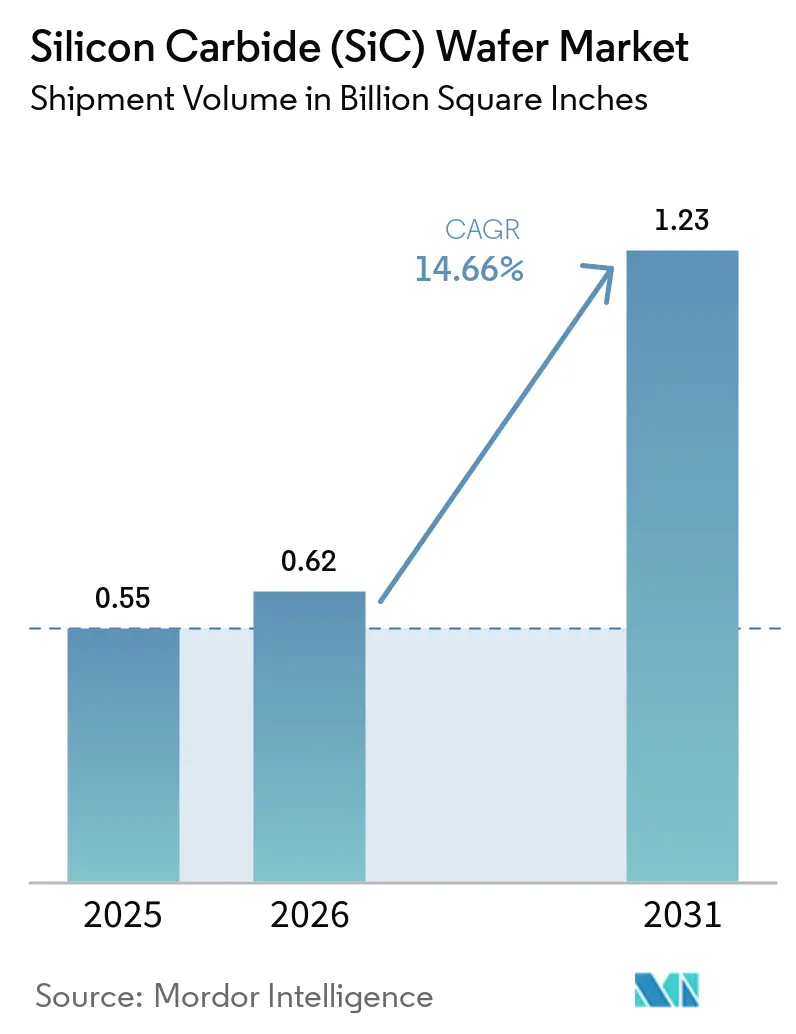
| Market Volume (2026) | 0.62 Billion Square Inches |
| Market Volume (2031) | 1.23 Billion Square Inches |
| Growth Rate (2026 - 2031) | 14.66% CAGR |
| Fastest Growing Market | Asia Pacific |
| Largest Market | Asia Pacific |
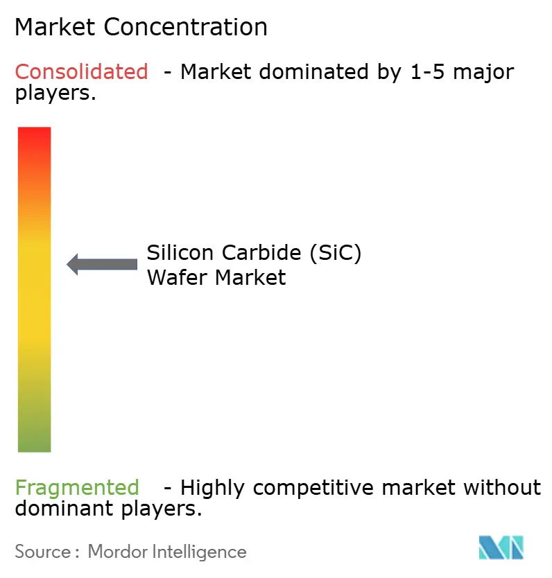
| Market Concentration | Medium |
Major Players *Disclaimer: Major Players sorted in no particular order Image © Mordor Intelligence. Reuse requires attribution under CC BY 4.0. | |
Silicon Carbide (SiC) Wafer Market Analysis by Mordor Intelligence
The Silicon Carbide (SiC) Wafer Market size was valued at 0.55 billion square inches in 2025 and is estimated to grow from 0.62 billion square inches in 2026 to reach 1.23 billion square inches by 2031, at a CAGR of 14.66% during 2026-2031. Rapid electrification of vehicles, grid-scale rollouts of renewable energy, and 5G radio-frequency front ends are steadily shifting demand toward wide-bandgap substrates that outperform silicon in high-temperature and high-frequency environments. Automakers adopting 800-volt platforms, charging-network operators installing 350-kilowatt dispensers, and policymakers subsidizing domestic fabs collectively expand the addressable base for the SiC wafer market. Competition among vertically integrated device manufacturers has intensified as Chinese suppliers scale 8-inch capacity and reduce 6-inch pricing, prompting Western peers to fast-track 200-millimeter ramps. Supply-chain fragmentation, export-control friction, and capital-intensive furnace lead times temper near-term growth but reinforce long-term regional diversification strategies.
Key Report Takeaways
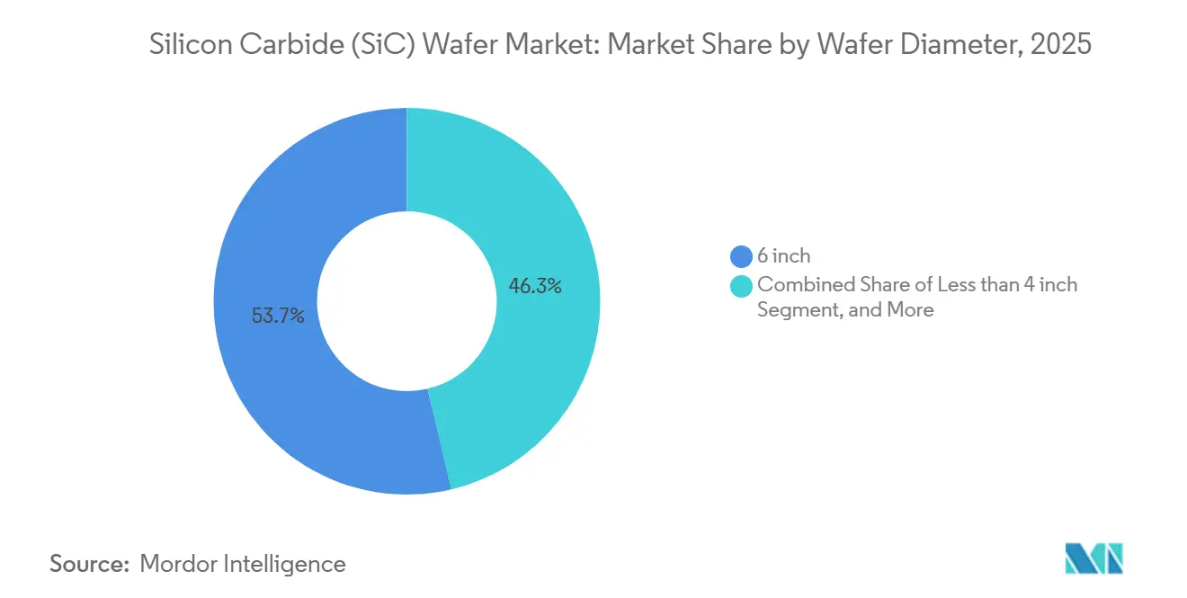
- By wafer diameter, 6-inch substrates held 53.69% of the SiC wafer market share in 2025, while 8-inch substrates are advancing at a 14.91% CAGR through 2031.
- By conductivity type, n-type wafers captured 68.32% of volume in 2025, and semi-insulating material is the fastest-growing category at a 15.06% CAGR.
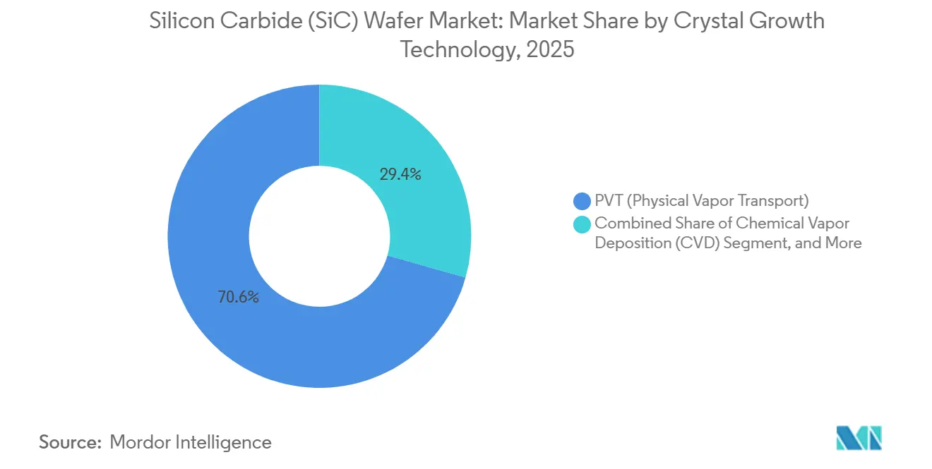
- By crystal-growth technology, physical vapor transport retained 70.61% of production in 2025, whereas chemical vapor deposition leads growth at 15.05% through 2031.
- By application, power electronics led with a 47.15% revenue share in 2025, and radio-frequency devices recorded the highest projected CAGR of 15.22% to 2031.
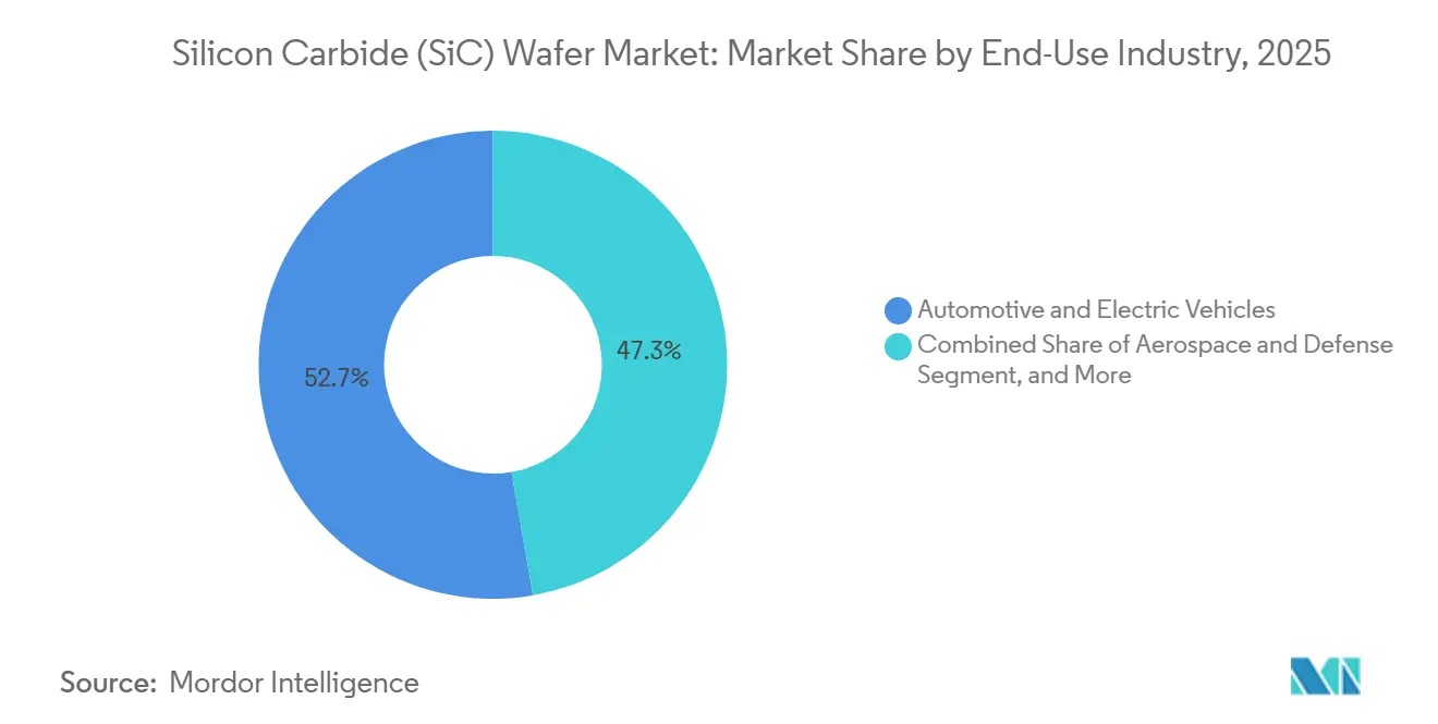
- By end-use industry, automotive and electric vehicles accounted for 52.73% of substrate area in 2025, while renewable energy and storage is expanding at a 15.28% CAGR.
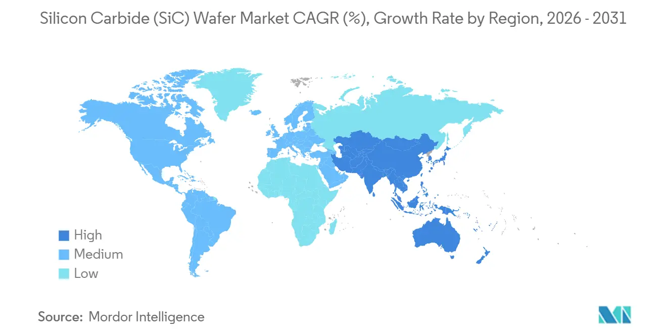
- By geography, Asia-Pacific commanded 63.75% of global volume in 2025 and is projected to maintain a 15.34% CAGR to 2031.
Note: Market size and forecast figures in this report are generated using Mordor Intelligence’s proprietary estimation framework, updated with the latest available data and insights as of 2026.
Global Silicon Carbide (SiC) Wafer Market Trends and Insights
Drivers Impact Analysis*
| Driver | (~) % Impact on CAGR Forecast | Geographic Relevance | Impact Timeline |
|---|---|---|---|
| Rising EV penetration and shift toward 800-volt vehicle platforms | +3.5% | Global, concentrated in China, Europe, North America | Medium term (2-4 years) |
| Rapid build-out of 800-volt charging infrastructure | +2.2% | Europe and China lead, North America accelerating | Medium term (2-4 years) |
| High-temperature, high-frequency performance advantages over silicon | +2.8% | Global | Long term (≥ 4 years) |
| Government incentives for wide-band-gap fabs | +2.5% | North America, Europe, Japan | Short term (≤ 2 years) |
| Vertical monolithic integration strategies compressing supply-chain costs | +1.5% | Global, led by Asia-Pacific and North America | Medium term (2-4 years) |
| AI-driven crystal-defect prediction improving 200-millimeter yields | +1.2% | Global, early adoption in Asia-Pacific and North America | Long term (≥ 4 years) |
| Source: Mordor Intelligence | |||


Rising EV Penetration and Shift Toward 800-Volt Vehicle Platforms
Electric-vehicle manufacturers are standardizing 800-volt architectures to reduce recharge times and wiring weight, locking SiC devices into traction inverters and on-board chargers, Porsche, Hyundai, Kia, and Lucid deployed SiC MOSFETs during 2024-2025, and General Motors will roll out 800-volt systems across the Ultium range in 2026. Toyota’s early-2025 wafer-allocation deal with Wolfspeed underscores that even hybrid-focused automakers accept wide-band-gap efficiency gains. Chinese regulators encourage domestic brands to adopt 800-volt designs, accelerating local substrate demand. Commercial-vehicle programs evaluating SiC for electric buses and delivery vans broaden the consumption base. The result is a durable pull that supports double-digit expansion for the SiC wafer market.
Rapid Build-out of 800 V Charging Infrastructure
Network operators are installing 350-kilowatt chargers that rely on SiC power stages to manage thermal and switching losses at high current. Europe’s IONITY extended its ultra-fast corridor in 2025, China’s State Grid added more than 10,000 dispensers the same year, and the United States committed USD 5 billion for fast-charging corridors through 2026.[1]U.S. Department of Energy, “National Electric Vehicle Infrastructure Program Guidance,” energy.gov Field data show SiC-based chargers achieve 15% lower downtime than silicon IGBT equivalents, improving utilization economics. Greater charger availability justifies vehicle-platform upgrades, closing a feedback loop that expands the SiC wafer market.
High-Temperature, High-Frequency Performance Advantages over Silicon
Silicon carbide’s 3.3-electronvolt band gap and superior thermal conductivity enable switching above 100 kilohertz and junction temperatures near 200 °C, shrinking passive components by up to 60% and cutting system weight. Industrial motor drives, railway traction, and aerospace power units capitalize on these attributes to improve efficiency and reliability. Radiation hardness attracts satellite and defense designers seeking single-event-upset immunity. These intrinsic advantages make SiC a long-term replacement rather than a transitional technology, extending growth prospects for the SiC wafer market.
Government Incentives for Wide-Band-Gap Fabs
Subsidies lower entry barriers for domestic production, diversify supply, and accelerate scaling to 200-millimeter formats. The United States CHIPS and Science Act awarded Wolfspeed USD 750 million in grants and USD 750 million in loan guarantees, while SK Siltron secured a USD 544 million federal loan for Michigan expansion.[2]U.S. Department of Commerce, “CHIPS and Science Act Awards to Wolfspeed,” commerce.gov Europe’s Chips Act allocated EUR 43 billion (USD 48 billion) for semiconductor projects, including EUR 3 billion (USD 3.3 billion) for Bosch’s Dresden line. Japan’s economic-security program channels funds to Resonac and ROHM to double domestic output. These policies compress payback periods, catalyze capacity additions, and support regional resilience, bolstering the outlook for the SiC wafer market.
Restraints Impact Analysis*
| Restraint | (~) % Impact on CAGR Forecast | Geographic Relevance | Impact Timeline |
|---|---|---|---|
| Limited availability of 200-millimeter substrates | -1.8% | Global, acute in North America and Europe | Short term (≤ 2 years) |
| Capital-intensive crystal-growth equipment | -1.5% | Global, barrier for new entrants | Medium term (2-4 years) |
| Post-polish micro-scratching causing latent device failures | -0.8% | Global | Medium term (2-4 years) |
| Geopolitical export-control risks on SiC equipment | -1.0% | China, North America, Europe | Short term (≤ 2 years) |
| Source: Mordor Intelligence | |||
Limited Availability of 200 mm Substrates
Demand for 200-millimeter formats exceeds crystal-growth capacity because furnace lead times run 18-24 months and yields hover near 70% in early production. Wolfspeed’s 2025 SEC filing cited yield shortfalls that delayed automotive qualifications.[3]U.S. Securities and Exchange Commission, “Wolfspeed Form 10-K FY 2025,” sec.gov STMicroelectronics and Infineon introduced 200-millimeter products in 2025, but together met less than half of automakers’ sample requests. Polishing bottlenecks adds complexity, with chemical-mechanical planarization tools on order backlogs until 2027. The shortage constrains near-term volume for the SiC wafer market and sustains price volatility.
Capital-Intensive Crystal-Growth Equipment
Building a greenfield SiC wafer plant costs USD 1-2 billion, and individual physical-vapor-transport furnaces exceed USD 5 million. Bosch’s Dresden project earmarked EUR 3 billion (USD 3.3 billion) for a 200-millimeter line, a sum feasible mainly for multinational firms or state-backed groups. Energy consumption at 2,300 °C raises operating costs and carbon-compliance fees. Subsidized electricity and land allow Chinese entrants such as Tankeblue to offer 6-inch wafers at USD 400-500, pressuring Western suppliers. High capital intensity slows new entrant formation and concentrates power among established players, capping competitive diversity in the SiC wafer market.
*Our forecasts treat driver/restraint impacts as directional, not additive. The impact forecasts reflect baseline growth, mix effects, and variable interactions.
Segment Analysis
By Wafer Diameter: Transition to Larger Formats Accelerates
Six-inch material held 53.69% of the SiC wafer market share in 2025, reflecting mature automotive qualifications. Eight-inch capacity is expanding at a 14.91% CAGR, driven by economies of scale that lower per-die cost. Wolfspeed’s January 2026 300-millimeter boule proof-point signaled a future step change, potentially adding 2.25 times the die count of 200-millimeter wafers. Formats below 4 inches continue in niche optoelectronics but lose relevance as radio-frequency makers move to 6-inch templates.
The shift upward is gated by furnace availability and thermal-stress control. STMicroelectronics raised 200-millimeter yields to 75% by integrating real-time temperature profiling. SK Siltron plans 30,000 eight-inch wafers per month in Michigan by late 2026, promising regional supply security. Automotive qualification inertia locks legacy platforms on 6-inch sizes, yet next-generation trucks and energy-storage systems are already designed-in with larger diameters. Consequently, the SiC wafer market size for eight-inch substrates is set to outpace overall growth.


By Conductivity Type: N-Type Dominance and Semi-Insulating Growth
N-type conductive wafers supplied 68.32% of volume in 2025, underpinning power-electronics devices that prioritize low on-resistance. Semi-insulating material is growing 15.06% annually as 5G, satellite, and radar customers pursue low-loss radio-frequency front ends. Premiums of 30-40% over n-type equivalents compensate for tighter purity and lower output, lifting revenue contribution beyond volume share.
China’s 5G rollout and United States defense funding both pull semi-insulating demand upward. Domestic Chinese champions such as SICC are investing in vanadium-doped growth processes, while the U.S. Defense Production Act funds pilot lines at Wolfspeed. N-type players continue to reap scale advantages, achieving nitrogen-doping uniformity below 5% across 200-millimeter wafers. Divergent growth trajectories keep both conductivity classes vital to the SiC wafer market.
By Crystal-Growth Technology: PVT Leads, CVD Gains in Epitaxy
Physical vapor transport supplied 70.61% of wafers in 2025 thanks to scalability, yet chemical vapor deposition registers a 15.05% CAGR as device makers seek thicker, low-defect epitaxial layers. PVT boules still carry micropipe densities above 1,000 defects/cm² in lower-grade lots, constraining higher-voltage yields. CVD reactors from Aixtron and LPE deliver uniform 10-50 µm films and less than 3% doping variation, supporting 1,200-volt designs.
Resonac’s AI-driven defect prediction has boosted 200-millimeter PVT yield by 12% and saved roughly USD 50 per wafer. Infineon’s CVD investment following its GaN Systems acquisition illustrates a trend toward hybrid vertical integration. As standards mature, the SiC wafer industry will likely maintain a dual-technology model balancing cost and performance.
By Application: Power Electronics Leads, RF Devices Surge
Power electronics absorbed 47.15% of substrate area in 2025, anchored by automotive traction inverters and grid-scale renewable inverters that operate above 100 kHz and 175 °C. Radio-frequency devices, though using smaller area, are climbing at a 15.22% CAGR as 5G base-station deployments and low-Earth-orbit constellations scale. Semi-insulating 6-inch wafers for GaN-on-SiC amplifiers command prices between USD 800 and USD 1,000, twice n-type power equivalents.
Optoelectronics and ultraviolet LEDs retain niche but profitable demand, while emerging sensor and quantum-computing research receives public grants. The SiC wafer market size tied to power electronics will remain dominant, but radio-frequency growth adds diversification and value uplift.
By End-Use Industry: Automotive Dominates, Renewables Accelerate
Automotive and electric-vehicle programs accounted for 52.73% of substrate consumption in 2025, a figure that locks in multi-year wafer demand due to 18-24 month qualification cycles. Renewable energy and storage are the fastest-growing segment, with a 15.28% CAGR, as solar and wind operators standardize 98-99% efficient SiC inverters. Long-term supply contracts, such as Toyota’s 2025 pact with Wolfspeed, give substrate makers revenue visibility but also enforce steep cost-down roadmaps.
Telecommunications and industrial motor drives demonstrate that electrification trends extend beyond vehicles. Aerospace and defense, although low in volume, secure premium pricing for radiation-hardened modules. Collectively, these verticals broaden the SiC wafer market and buffer it from automotive cyclicality.
Geography Analysis
Asia-Pacific supplied 63.75% of all substrate area in 2025 and is set to post a 15.34% CAGR through 2031 as China funds domestic fabs and Japan extends crystal-growth leadership. China’s National Integrated Circuit Fund committed CNY 50 billion (USD 7 billion) to SiC over 2024-2025, enabling Tankeblue to start an eight-inch line producing 600,000 wafers annually. Japan’s Resonac and ROHM doubled 150-millimeter and 200-millimeter capacity, shipping material to automakers in North America and Europe that seek non-Chinese supply.
North America is expected to see significant output growth by 2025, driven by companies such as Wolfspeed and Coherent. CHIPS Act grants and Department of Energy loans are anticipated to boost regional capacity to over 100,000 wafers per month by late 2026, strengthening supply security for defense and EV programs. Europe is also projected to experience growth in output by 2029 on the back of Bosch’s Dresden plant and STMicroelectronics’ Catania expansion, both aided by the EUR 43 billion (USD 48 billion) EU Chips Act.
The Middle East and Africa, plus South America, remain early-stage. Saudi Arabia’s Public Investment Fund is studying a domestic fab under Vision 2030, while Brazil’s development bank assesses financing for a joint venture serving regional renewables and EVs. Diverse subsidy regimes, export-control measures, and energy-price differentials will keep the SiC wafer market geographically fluid through the forecast horizon.

Competitive Landscape
The top five suppliers-Wolfspeed, Coherent, STMicroelectronics, ROHM, and SK Siltron-controlled about half of global capacity in 2025, indicating moderate market concentration. Chinese entrants such as Tankeblue and Guangdong TySiC have grown rapidly by leveraging subsidized utilities and offering 6-inch wafers at USD 400-500, forcing incumbents to differentiate on defect density and technical support rather than price. Vertical integration is the dominant competitive tactic; Infineon’s 2024 acquisition of GaN Systems aligned wafer, epitaxy, and device capabilities under one roof.
Technology has become a key front. AI-enabled process control lifted 200-millimeter yields 10-15 percentage points in early deployments, trimming scrap and freeing latent capacity. Wolfspeed’s 300-millimeter boule demonstration in January 2026 positions the company to establish de facto standards as customers validate the format.
Patent filings exceeded 200 in 2025, signifying accelerating innovation cycles. The SiC wafer market is therefore defined by a combination of capacity race, yield leadership, and strategic control of key process intellectual property.
Silicon Carbide (SiC) Wafer Industry Leaders
Wolfspeed Inc.
Coherent Corp. (II-VI Incorporated)
STMicroelectronics (Norstel AB)
Rohm Semiconductor GmbH
SK Siltron Co., Ltd.
- *Disclaimer: Major Players sorted in no particular order

Recent Industry Developments
- January 2026: Wolfspeed announced the successful growth of the first 300-millimeter SiC boule, targeting pilot customer qualifications by late 2027.
- September 2025: Wolfspeed, Inc. officially launched its 200mm SiC material products, a pivotal step in the company's quest to hasten the industry's shift from silicon-to-silicon carbide.
- June 2025: With the launch of its new 8-inch (200-mm) SiC wafer production line, Singapore has solidified its standing in the dynamic global semiconductor arena.
- February 2025: Toyota and Wolfspeed entered a long-term wafer-supply agreement for next-generation battery-electric platforms.


Global Silicon Carbide (SiC) Wafer Market Report Scope
The Silicon Carbide (SiC) Wafer Market is Segmented by Wafer Diameter (Less than 4 inch, 6 inch, 8 inch, and Above 12 inch), Conductivity Type (N-type Conductive and Semi-insulating), Application (Power Electronics, Radio-Frequency Devices, Optoelectronics and LED, and Other Applications), End-use Industry (Automotive and Electric Vehicles, Renewable Energy and Storage, Telecommunications, Industrial Motor Drives and UPS, Aerospace and Defense, and Other End-user Industries), Crystal-Growth Technology (Physical Vapor Transport, Chemical Vapor Deposition, Modified Lely Sublimation, and Other Technologies), and Geography (North America, South America, Europe, Asia-Pacific, and Middle East and Africa). The Market Forecasts are Provided in Terms of Volume (Square Inches).
| Less than 4 inch |
| 6 inch |
| 8 inch |
| Above 12 inch |
| N-type Conductive |
| Semi-insulating |
| Power Electronics |
| Radio-Frequency Devices |
| Optoelectronics and LED |
| Other Applications |
| Automotive and Electric Vehicles |
| Renewable Energy and Storage |
| Telecommunications |
| Industrial Motor Drives and UPS |
| Aerospace and Defense |
| Other End-user Industries |
| Physical Vapor Transport (PVT) |
| Chemical Vapor Deposition (CVD) |
| Modified Lely Sublimation |
| Other Technologies |
| North America | United States | |
| Canada | ||
| South America | Brazil | |
| Argentina | ||
| Rest of South America | ||
| Europe | Germany | |
| France | ||
| United Kingdom | ||
| Italy | ||
| Spain | ||
| Rest of Europe | ||
| Asia-Pacific | China | |
| Japan | ||
| South Korea | ||
| Taiwan | ||
| India | ||
| Rest of Asia-Pacific | ||
| Middle East and Africa | Middle East | Saudi Arabia |
| United Arab Emirates | ||
| Rest of Middle East | ||
| Africa | South Africa | |
| Nigeria | ||
| Rest of Africa | ||
| By Wafer Diameter | Less than 4 inch | ||
| 6 inch | |||
| 8 inch | |||
| Above 12 inch | |||
| By Conductivity Type | N-type Conductive | ||
| Semi-insulating | |||
| By Application | Power Electronics | ||
| Radio-Frequency Devices | |||
| Optoelectronics and LED | |||
| Other Applications | |||
| By End-use Industry | Automotive and Electric Vehicles | ||
| Renewable Energy and Storage | |||
| Telecommunications | |||
| Industrial Motor Drives and UPS | |||
| Aerospace and Defense | |||
| Other End-user Industries | |||
| By Crystal-Growth Technology | Physical Vapor Transport (PVT) | ||
| Chemical Vapor Deposition (CVD) | |||
| Modified Lely Sublimation | |||
| Other Technologies | |||
| By Geography | North America | United States | |
| Canada | |||
| South America | Brazil | ||
| Argentina | |||
| Rest of South America | |||
| Europe | Germany | ||
| France | |||
| United Kingdom | |||
| Italy | |||
| Spain | |||
| Rest of Europe | |||
| Asia-Pacific | China | ||
| Japan | |||
| South Korea | |||
| Taiwan | |||
| India | |||
| Rest of Asia-Pacific | |||
| Middle East and Africa | Middle East | Saudi Arabia | |
| United Arab Emirates | |||
| Rest of Middle East | |||
| Africa | South Africa | ||
| Nigeria | |||
| Rest of Africa | |||


Key Questions Answered in the Report
What is the projected volume for global SiC wafers by 2031?
The SiC wafer market is forecast to reach 1.23 billion square inches by 2031, expanding at a 14.66% CAGR from 2026.
Which wafer diameter is growing fastest?
Eight-inch substrates post the highest growth, registering a 14.91% CAGR through 2031 as manufacturers chase lower per-die costs.
Why are automakers shifting to SiC devices?
SiC enables 800-volt vehicle architectures that cut recharge times to about 10 minutes and improve drivetrain efficiency, making it the preferred material for traction inverters.t.
How are governments supporting domestic SiC supply?
Subsidy programs such as the U.S. CHIPS Act, the EU Chips Act, and Japan’s economic-security incentives provide direct funding, tax credits, and loans to expand 200-millimeter production capacity.
Which end-use vertical is expanding fastest outside automobiles?
Renewable energy and storage applications are advancing at a 15.28% CAGR as solar and wind installations adopt SiC-based inverters for 98-99% efficiency.
Page last updated on:


