
Semiconductor Manufacturing Equipment Market Size and Share
Market Overview
| Study Period | 2020 - 2031 |
|---|---|
| Market Size (2026) | USD 168.45 Billion |
| Market Size (2031) | USD 283.21 Billion |
| Growth Rate (2026 - 2031) | 10.95 % |
| Fastest Growing Market | Asia-Pacific |
| Largest Market | Asia-Pacific |
| Market Concentration | Medium |
Major Players *Disclaimer: Major Players sorted in no particular order Image © Mordor Intelligence. Reuse requires attribution under CC BY 4.0. | |
Semiconductor Manufacturing Equipment Market Analysis by Mordor Intelligence
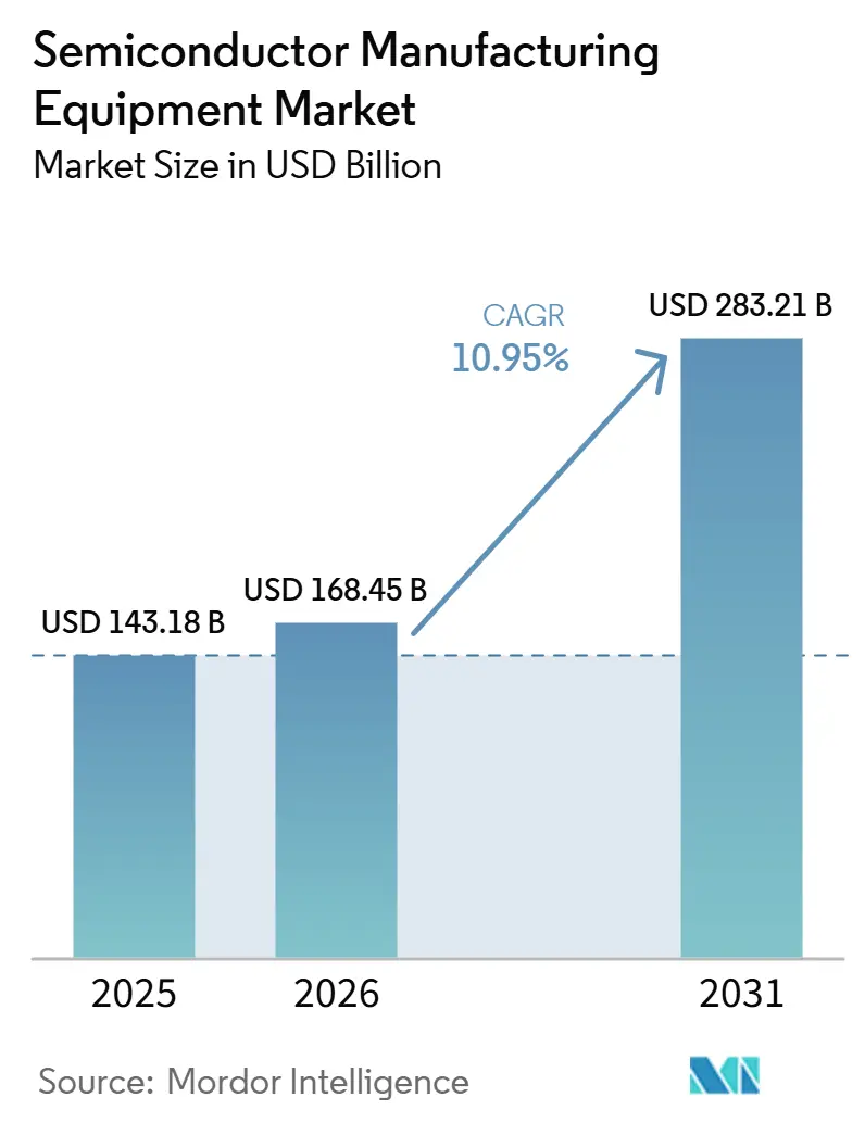
The Semiconductor Manufacturing Equipment Market size is expected to increase from USD 143.18 billion in 2025 to USD 168.45 billion in 2026 and reach USD 283.21 billion by 2031, growing at a CAGR of 10.95% over 2026-2031.
Global semiconductor manufacturing equipment billings are expected to register year-over-year growth in 2025. Continued investments in advanced logic, memory, and AI-related manufacturing capacity are driving this growth across front-end wafer fabrication and back-end assembly, packaging, and test equipment. The semiconductor manufacturing equipment market is benefiting from simultaneous capital spending on logic and memory, rather than the alternating investment cycles that previously shaped equipment demand. Rising process complexity is also increasing the number of manufacturing steps per wafer, thereby supporting demand for lithography, deposition, etch, metrology, inspection, test, and advanced packaging tools, even without proportional expansion in wafer capacity. However, export controls, project execution timelines, supply chain constraints, and the availability of skilled labor will affect how quickly announced investments translate into equipment installations.
Key Report Takeaways
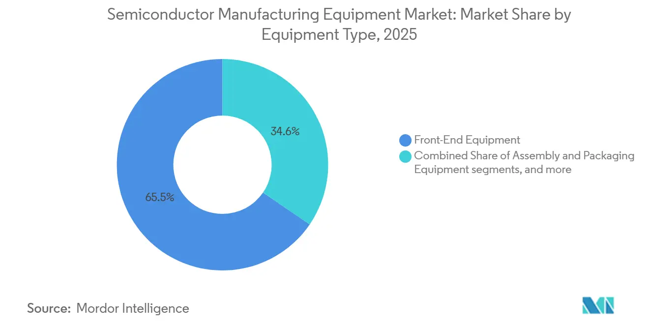
- By equipment type, wafer fab equipment/front-end equipment accounted for 65.45% of the semiconductor manufacturing equipment market share in 2025, while assembly and packaging equipment are projected to be the fastest-growing, with a 13.50% CAGR through 2031.
- By device type, logic and microcomponents accounted for 31.50% of the semiconductor manufacturing equipment market size in 2025, while the memory segment is projected to be the fastest-growing, with a 12.95% CAGR through 2031.
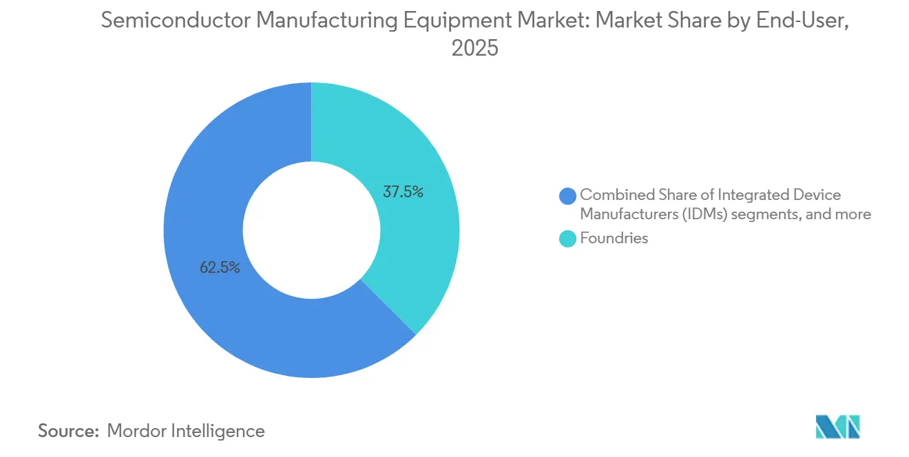
- By end user, the foundries segment accounted for 37.5% of the market in 2025 and is expected to remain the fastest-growing segment, with a 12.70% CAGR through 2031.
- By geography, Asia-Pacific held the leading position in the semiconductor manufacturing equipment industry, accounting for 64.35% of the market share in 2025, and is expected to remain the fastest-growing regional segment at a 12.30% CAGR through 2031.
Note: Market size and forecast figures in this report are generated using Mordor Intelligence’s proprietary estimation framework, updated with the latest available data and insights as of January 2026.
Market Trends and Insights
Drivers Impact Analysis of Semiconductor Manufacturing Equipment Market*
| Driver | (~) % Impact on CAGR Forecast | Geographic Relevance | Impact Timeline |
|---|---|---|---|
| AI, HBM, Chiplets, and Advanced Packaging Demand | +4.0% | Global, led by Taiwan, South Korea, and North America | Short term (≤ 2 years) |
| Advanced Node Migration and Rising Process Complexity | +2.5% | Taiwan, South Korea, Japan, and North America | Medium term (2-4 years) |
| Memory Technology Upgrades and HBM Capacity Expansion | +2.0% | South Korea, Japan, and China | Short term (≤ 2 years) |
| Government Fab Localization and Subsidy Programs | +1.5% | Global, including the United States, Europe, Japan, India, and South Korea | Long term (≥ 4 years) |
| Multi-Region Fab Capacity Expansion | +1.0% | North America, Europe, Japan, India, and Singapore | Medium term (2-4 years) |
| Mature-Node, Power Semiconductor, and Specialty Fab Investments | +0.8% | Europe, China, and North America | Long term (≥ 4 years) |
| Source: Mordor Intelligence | |||
AI, HBM, Chiplets, and Advanced Packaging Demand
AI accelerators, high-bandwidth memory, chiplets, and advanced packaging are changing the pattern of equipment investment. SEMI projected USD 52 billion in global 300 mm memory fab equipment spending for 2026, with DRAM equipment spending expected to reach USD 37 billion. The semiconductor manufacturing equipment market benefits from HBM production, which requires specialized processes for etch, deposition, fill, inspection, and packaging. These requirements add tool demand before considering any increase in memory output. Chiplet designs also increase the need for precise die placement, bonding, test, and inspection. This driver is strongest in Taiwan, South Korea, and North America, where leading logic and memory capacity is concentrated. It provides the semiconductor manufacturing equipment market with sustained exposure to high-value manufacturing and packaging investments.[1]SEMI, “SEMI Reports Global Semiconductor Equipment Billings Reached USD 135 Billion in 2025, Up 15% Year-on-Year,” SEMI, semi.org.
Advanced Node Migration and Rising Process Complexity
The move toward 2 nm gate-all-around designs increases the number and precision of fabrication steps. SEMI expects foundry and logic wafer fab equipment spending to reach USD 78 billion in 2026, up 18.9% from 2025. Gate-all-around structures require more selective etch and deposition work than earlier FinFET designs. Each additional step can also increase the need for metrology and process-control equipment. Intel Foundry used ASML's High NA EUV system for a high-volume logic product in July 2026, demonstrating that new lithography platforms are entering production. The semiconductor manufacturing equipment market, therefore, benefits from higher equipment intensity as manufacturers move to more complex process nodes. This leaves the semiconductor manufacturing equipment market less dependent on new fab buildings alone.
Memory Technology Upgrades and HBM Capacity Expansion
Memory investment remained important in 2025 as demand shifted toward HBM and newer DRAM and NAND architectures. SEMI reported that memory-related semiconductor capital expenditure rose 57% year over year in the first quarter of 2025, compared with 15% growth in non-memory capital expenditure. SEMI forecasts DRAM wafer fab equipment spending of USD 38.8 billion and NAND wafer fab equipment spending of USD 13.9 billion in 2026. HBM introduces processes for through-silicon vias, barrier metals, and dielectric fill that are not interchangeable with those used in earlier memory production methods. These changes limit the ability to reuse older tools and encourage fresh procurement. The semiconductor manufacturing equipment market consequently faces exposure to architectural upgrades and capacity additions. The semiconductor manufacturing equipment market also benefits when new memory standards require distinct process flows.
Government Fab Localization and Subsidy Programs
Government programs are supporting domestic fabrication projects in several regions. The United States CHIPS and Science Act provided USD 52.7 billion for semiconductor research, development, and manufacturing. The Section 48D investment tax credit is available for qualifying projects that begin construction by December 31, 2026. The European Commission proposed the Chips Act 2.0 in June 2026, extending policy attention to chiplets, photonic chips, and neuromorphic technologies. India also reported that 10 projects under the Semicon India Programme had been approved by 2026. The semiconductor manufacturing equipment market receives a longer equipment order pipeline as subsidized sites move from construction into tool installation. These programs make the semiconductor manufacturing equipment market more geographically diverse over time.
Restraints Impact Analysis of Semiconductor Manufacturing Equipment Market*
| Restraint | (~) % Impact on CAGR Forecast | Geographic Relevance | Impact Timeline |
|---|---|---|---|
| Export Controls, Tariffs, and Trade Fragmentation | -2.0% | Global, including China, Japan, the Netherlands, South Korea, and North America | Short term (≤ 2 years) |
| Semiconductor Capex Cyclicality and Fab Investment Delays | -1.5% | Global | Medium term (2-4 years) |
| Supplier Bottlenecks in Optics, Vacuum, Precision Components, and Specialty Inputs | -0.8% | Japan, Germany, and the Netherlands | Medium term (2-4 years) |
| Extreme Tool Cost, Long Lead Times, and Long Payback Cycles | -0.5% | Global | Short term (≤ 2 years) |
| Source: Mordor Intelligence | |||
Export Controls, Tariffs, and Trade Fragmentation
Export controls have narrowed the range of equipment and related technologies that can be supplied to certain destinations. In December 2024, the United States Bureau of Industry and Security added controls covering 24 types of semiconductor manufacturing equipment, 3 types of semiconductor development software, HBM-related rules, and 140 additions to the Entity List. A January 2025 interim final rule extended licensing requirements for certain advanced computing integrated circuits and covered manufacturing routes. These rules create compliance requirements for suppliers and customers across several countries. They can affect product configuration, customer qualification, shipment timing, and service arrangements. The semiconductor manufacturing equipment market also faces the risk that restrictions support the development of alternative domestic supply chains.[2]U.S. Government Accountability Office, “Export Controls, Commerce Implemented Advanced Semiconductor Rules,” U.S. Government Accountability Office, gao.gov.
Semiconductor Capex Cyclicality and Fab Investment Delays
Semiconductor capital spending remains exposed to demand cycles, project execution, and customer investment decisions. The Congressional Research Service documented that scheduled production dates for several CHIPS Act-supported fabrication projects extend into the late 2020s and 2030s. The National Network for Microelectronics Education projected a United States semiconductor workforce gap of 127,000 to 157,000 workers by 2030. This gap can postpone construction, commissioning, and production ramps even when project funding is available. Delays may push equipment deliveries into later periods rather than eliminating demand. The semiconductor manufacturing equipment market must therefore balance a strong project pipeline against the practical timing of fab completion and workforce readiness.
*Our forecasts treat driver/restraint impacts as directional, not additive. The impact forecasts reflect baseline growth, mix effects, and variable interactions.
Semiconductor Manufacturing Equipment Market Segment Analysis
By Equipment Type:
Front-End Demand and Assembly and Packaging Equipment Complexity Support Tool InvestmentFront-end equipment accounted for 65.45% of the market share in 2025. It remained the main driver of spending because advanced logic and memory fabs require lithography, deposition, etch, cleaning, planarization, thermal processing, metrology, and inspection. SEMI forecasts wafer fab equipment spending of USD 143.9 billion in 2026, a 23.1% rise from 2025. The semiconductor manufacturing equipment market size is supported by leading-edge logic and memory capacity, as well as by more demanding process flows. Applied Materials introduced deposition and selective-etch systems in June 2026 for deep, narrow 3D structures used in advanced logic and memory. ASML also plans to continue expanding EUV and DUV capacity to serve customer demand. These actions show that front-end demand includes both new capacity and tool replacement at more advanced nodes.[3]ASML, “ASML Reports EUR 32.7 Billion Total Net Sales and EUR 9.6 Billion Net Income in 2025,” ASML, asml.com.
Assembly, packaging, and test equipment registered the fastest 13.50% CAGR in the semiconductor manufacturing equipment industry through 2031 and have become increasingly important as AI devices and HBM stacks require more complex back-end operations. SEMI reported that test equipment increased 55% in 2025 and projected USD 15.3 billion in test equipment sales for 2026. Packaging equipment also supports hybrid bonding, die attach, substrate inspection, and other specialized work. Applied Materials introduced systems for through-silicon via fill, microbump formation, and defect analysis in June 2026. Fab facility, automation, and support equipment remain necessary for greenfield sites that require chemical delivery, gas systems, material handling, and cleanroom infrastructure. Together, these activities broaden demand for equipment beyond the primary wafer-processing stage.



By Device Type:
Logic and Memory Architecture Changes Increase Equipment NeedsLogic and micro components accounted for 31.50% of the market share in 2025, and support investment in advanced-node manufacturing for high-performance computing, AI processors, and premium mobile devices. SEMI projected USD 78 billion in foundry and logic wafer fab equipment spending for 2026. The semiconductor manufacturing equipment market is influenced by the transition to 2 nm gate-all-around manufacturing, which adds fabrication and control steps. Intel's use of High-NA EUV in a high-volume product demonstrates the growing role of new lithography tools. Microprocessors are part of this demand base, as established, and custom processor designs move to advanced process nodes. Analog, discrete, and power devices also continue to drive demand for mature-node equipment, although their purchasing patterns differ from those for leading-edge logic.
The memory segment recorded a 12.95% CAGR in the semiconductor manufacturing equipment industry through 2031, as upgrades to HBM, DRAM, and NAND architectures are shaping memory investment. SEMI projected that 2026 DRAM wafer fab equipment spending would reach USD 38.8 billion, while NAND spending would reach USD 13.9 billion. HBM requires more demanding processes for via formation, deposition, fill, assembly, and test. Higher-layer 3D NAND also increases the requirements for high-aspect-ratio etch and deposition systems. These technical changes create procurement needs that do not depend only on higher wafer starts. Sensors, MEMS, and optoelectronic devices reduce the need for specialized equipment as edge computing and sensing applications expand.
By End User:
Foundry and IDM Projects Shape Procurement ProgramsFoundries accounted for 37.5% of the semiconductor manufacturing equipment market share in 2025 and are expected to register a 12.70% CAGR through 2031. Foundries are major equipment buyers because they must maintain process leadership while serving multiple chip designers. TSMC reported having 18 to 12-inch wafer fabs under construction or renovation, including five advanced packaging facilities. This type of multi-site development supports the semiconductor manufacturing equipment market, as each facility requires an integrated set of processing and support tools. Samsung stated that its sub-8 nm lines were at full utilization and that 2 nm orders were expected to more than double in 2026. Competition among leading foundries can pull tool orders forward as companies prepare capacity for new technology generations. The same projects also require close coordination with utilities, construction teams, and local workforces.
Integrated device manufacturers remain important customers for memory, power, analog, and specialty semiconductor tools. The United States Department of Commerce announced up to USD 6.1 billion in proposed CHIPS incentives for Micron projects in New York and Idaho. Bosch reached a definitive funding agreement for up to USD 225 million as part of a USD 2 billion silicon carbide project in California. Outsourced semiconductor assembly and test providers are also increasing their use of advanced packaging, bonding, and inspection systems. Research and pilot lines provide early demand for newer platforms, such as High-NA EUV and panel-level packaging tools. These users help qualify equipment before broader production deployment.
Geography Analysis
APAC Semiconductor Manufacturing Equipment Market
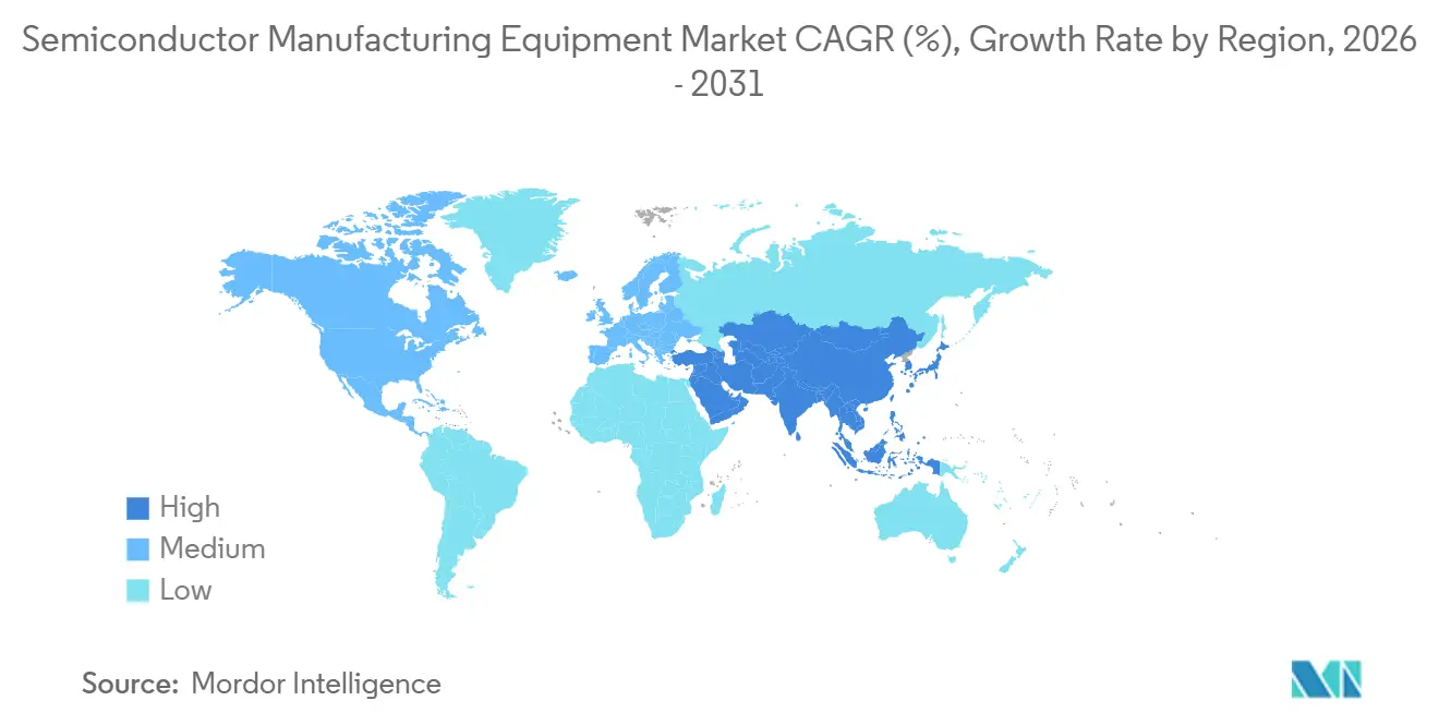
Asia-Pacific accounted for 64.35% of the market share in 2025 and is expected to remain the largest regional market for semiconductor manufacturing equipment, registering a 12.30% CAGR, led by China, Taiwan, South Korea, and Japan, which together account for the majority of global equipment billings. Taiwan is projected to record USD 31.5 billion in semiconductor equipment billings, a 90% increase from 2024, driven by continued investments in advanced logic and advanced packaging capacity. South Korea is expected to reach USD 25.8 billion, up 26%, supported by expansions in HBM and DRAM capacity. Japan’s billings are projected to increase by 22% to USD 9.5 billion, as domestic fabrication projects and its established semiconductor materials and equipment ecosystem sustain capital investment. China is expected to remain the world’s largest equipment market, with USD 49.3 billion in billings, despite a marginal 0.5% decline, reflecting continued investment in mature-node manufacturing, specialty semiconductors, and domestic supply chain development.
North America, Europe and APAC Semiconductor Manufacturing Equipment Market
North America is projected to record USD 10.9 billion in equipment billings, down 20% year over year. However, the construction and commissioning of new fabs supported by the CHIPS and Science Act are expected to drive higher equipment installations as projects advance from site development to production. Europe generated USD 2.9 billion in billings in 2025, representing a 41% decline from 2024. However, the European Chips Act continues to support strategic investments in semiconductor manufacturing and technology expansion across the region. Emerging manufacturing hubs, including India through the Semicon India Programme and Singapore through investments in advanced packaging and specialty semiconductors, are strengthening their positions within the global semiconductor manufacturing ecosystem. Looking ahead, SEMI projects China, Taiwan, and South Korea to remain the three largest semiconductor equipment markets through 2031, reflecting the continued concentration of global wafer fabrication capacity and advanced-node investments.

Competitive Landscape
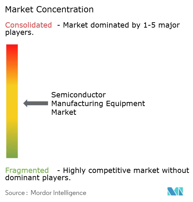
The semiconductor manufacturing equipment market has medium concentration, with a highly concentrated top tier in process-critical categories, including lithography, deposition, etch, and inspection. ASML reported net sales of EUR 32.7 billion (USD 36.90 billion) in 2025 and a year-end backlog of EUR 38.8 billion (USD 43.79 billion). Its plan to expand EUV and DUV capacity responds to customer demand for advanced-node production tools. Applied Materials reported USD 28.4 billion in fiscal 2025 revenue. Lam Research reported revenue of USD 18.4 billion in fiscal 2025. These companies compete through tool performance, production capacity, service coverage, and the ability to support increasingly complex device structures.
Process control has become more important as smaller features and 3D structures increase the cost of yield loss. KLA reported USD 12.2 billion in fiscal 2026 semiconductor process-control revenue, compared with USD 11.0 billion in fiscal 2025. ASML also invested EUR 1.3 billion (USD 1.46 billion) in metrology and inspection systems in 2025. Applied Materials introduced the SEMVision G7AP platform in June 2026 for defect analysis on advanced packaging substrates. These moves show that the competitive field extends beyond individual deposition or lithography tools. Suppliers are expanding into adjacent steps where customers need integrated processes and inspection capabilities.
Back-end equipment is attracting strategic investment because chiplets and HBM require packaging operations closer to front-end process control. Applied Materials introduced its Nokota VMax 2 system for through-silicon via fill and microbump formation in June 2026. ASML's deployment of High NA EUV with Intel Foundry is another strategic move that advances a new lithography category into production. Bosch's investment in silicon carbide manufacturing also reflects continued demand for specialty semiconductor equipment. Competition will depend on how quickly suppliers can qualify tools for new materials, 3D structures, and package formats. Export rules and customer qualification requirements may shape the addressable opportunity by region.
Semiconductor Manufacturing Equipment Industry Leaders
Applied Materials, Inc.
ASML Holding N.V.
Lam Research Corporation
Tokyo Electron Limited
KLA Corporation
- *Disclaimer: Major Players sorted in no particular order
Semiconductor Manufacturing Equipment Market Companies Covered in this Report
- Applied Materials, Inc.
- ASML Holding N.V.
- Lam Research Corporation
- Tokyo Electron Limited
- KLA Corporation
- SCREEN Holdings Co., Ltd.
- Advantest Corporation
- ASM International N.V.
- Teradyne, Inc.
- Hitachi High-Tech Corporation
- Onto Innovation Inc.
- Cohu, Inc.
- BE Semiconductor Industries N.V.
- EV Group
- Kokusai Electric Corporation
- ASMPT Limited
- ACM Research, Inc.
- Disco Corporation
- Canon Inc.
- Nikon Corporation
- Axcelis Technologies, Inc.
- Nova Ltd.
- Lasertec Corporation
- SUSS MicroTec SE
- Tokyo Seimitsu Co., Ltd. / ACCRETECH

Recent Industry Developments in Semiconductor Manufacturing Equipment Market
- July 2026: Applied Materials introduced the Nokota VMax 2 electrochemical deposition system for through-silicon-via fill and microbump formation, as well as the SEMVision G7AP platform for advanced packaging substrates. The systems address process requirements in advanced memory and logic packaging, where placement accuracy and defect analysis are important for production qualification.
- July 2026: ASML reported that High NA EUV had reached a production milestone through the first high-volume logic product using the technology. The announcement confirmed the use of the TwinScan EXE:5200B platform for Intel Core Ultra Series 3 processors and marked the first volume logic product produced with this technology.
- July 2026: Bosch announced a definitive CHIPS funding agreement for up to USD 225 million to support its silicon carbide manufacturing investment in Roseville, California. The agreement forms part of an up to USD 2 billion project to convert the site for 200 mm silicon carbide production, with commercial manufacturing scheduled to begin in 2026.
- July 2026: Infineon opened its Smart Power Fab in Dresden, Germany, following a EUR 5 billion (USD 5.64 billion) investment. The facility was opened ahead of schedule and will produce power semiconductors and analog and mixed-signal devices, adding capacity for automotive, energy, and industrial applications.


Global Semiconductor Manufacturing Equipment Market Report Scope
The Semiconductor Manufacturing Equipment Market Report is Segmented by Equipment Type (Wafer Fab Equipment / Front-End Equipment, and More), by Device Type (Logic and Micro-components, Memory, Analog, and More), by End-User (Integrated Device Manufacturers (IDMs), Foundries, and More), and by Geography (Asia-Pacific, Europe, and More). The Report Offers Market Size and Forecasts in Value (USD) for all the Above Segments.
| Wafer Fab Equipment / Front-End Equipment (lithography, deposition, etching, cleaning, CMP, thermal processing, front-end metrology & inspection equipment, etc.) |
| Assembly and Packaging Equipment (die attach, wire bonding, flip-chip bonding, wafer bumping, thinning, dicing, molding, etc.) |
| Semiconductor Test Equipment (automated test equipment, wafer probers, test handlers, burn-in equipment, and final test equipment) |
| Fab Facility, Automation and Support Equipment (automation systems, wafer handling systems, AMHS, chemical & gas delivery systems, chillers, cleanroom support equipment, etc.)) |
| Logic and Microcomponents (logic ICs, etc.) |
| Memory (DRAM, NAND, HBM, NOR, etc.) |
| Microprocessors (MPUs) |
| Analog (Power management ICs, signal chain, interface Ics, etc.) |
| Discrete and Power Devices (Diodes, transistors, MOSFETs, etc.) |
| Sensors, MEMS and Optoelectronic Devices (Image sensors, MEMS sensors, etc.) |
| Integrated Device Manufacturers (IDMs) |
| Foundries |
| Outsourced Semiconductor Assembly and Test (OSAT) Companies |
| Others (Research & Development (R&D) and Pilot Lines) |
| North America | United States |
| Canada | |
| Mexico | |
| South America | Brazil |
| Rest of South America | |
| Europe | Germany |
| France | |
| Ireland | |
| Italy | |
| Netherlands | |
| Rest of Europe | |
| Asia-Pacific | China |
| Taiwan | |
| South Korea | |
| Japan | |
| Singapore | |
| India | |
| Rest of Asia-Pacific | |
| Middle East and Africa |
| By Equipment Type | Wafer Fab Equipment / Front-End Equipment (lithography, deposition, etching, cleaning, CMP, thermal processing, front-end metrology & inspection equipment, etc.) | |
| Assembly and Packaging Equipment (die attach, wire bonding, flip-chip bonding, wafer bumping, thinning, dicing, molding, etc.) | ||
| Semiconductor Test Equipment (automated test equipment, wafer probers, test handlers, burn-in equipment, and final test equipment) | ||
| Fab Facility, Automation and Support Equipment (automation systems, wafer handling systems, AMHS, chemical & gas delivery systems, chillers, cleanroom support equipment, etc.)) | ||
| By Device Type | Logic and Microcomponents (logic ICs, etc.) | |
| Memory (DRAM, NAND, HBM, NOR, etc.) | ||
| Microprocessors (MPUs) | ||
| Analog (Power management ICs, signal chain, interface Ics, etc.) | ||
| Discrete and Power Devices (Diodes, transistors, MOSFETs, etc.) | ||
| Sensors, MEMS and Optoelectronic Devices (Image sensors, MEMS sensors, etc.) | ||
| By End User | Integrated Device Manufacturers (IDMs) | |
| Foundries | ||
| Outsourced Semiconductor Assembly and Test (OSAT) Companies | ||
| Others (Research & Development (R&D) and Pilot Lines) | ||
| By Geography | North America | United States |
| Canada | ||
| Mexico | ||
| South America | Brazil | |
| Rest of South America | ||
| Europe | Germany | |
| France | ||
| Ireland | ||
| Italy | ||
| Netherlands | ||
| Rest of Europe | ||
| Asia-Pacific | China | |
| Taiwan | ||
| South Korea | ||
| Japan | ||
| Singapore | ||
| India | ||
| Rest of Asia-Pacific | ||
| Middle East and Africa | ||


Key Questions Answered in the Report
How large is the semiconductor manufacturing equipment market in 2026?
The semiconductor manufacturing equipment market size is estimated at USD 168.45 billion in 2026 and is forecast to reach USD 283.21 billion by 2031.
What is driving semiconductor manufacturing equipment demand through 2031?
AI processors, HBM, advanced packaging, 2 nm logic migration, memory upgrades, and government-backed fab construction are supporting demand.
Why do advanced chip designs require more manufacturing equipment?
Gate-all-around logic, HBM, and 3D NAND require additional steps for etch, deposition, metrology, inspection, packaging, and testing.
Which regions are most important for equipment investment?
China, Taiwan, and South Korea remained the leading equipment destinations, while localization programs support North America, Europe, Japan, and India.
How do export controls affect equipment suppliers?
Controls can limit shipments, increase licensing and compliance work, and encourage the development of alternative regional supply chains.
What is the main execution risk for new semiconductor fabs?
Project schedules can be delayed by skilled-worker shortages, infrastructure needs, supply constraints, and changing capital expenditure plans.
Page last updated on:


 Your data is secure and never sold or shared.


