Semiconductor ICP-MS Systems Market Size and Share
Market Overview
| Study Period | 2019 - 2030 |
|---|---|
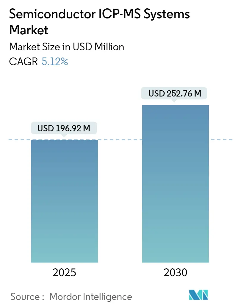
| Market Size (2025) | USD 196.92 Million |
| Market Size (2030) | USD 252.76 Million |
| Growth Rate (2025 - 2030) | 5.12% CAGR |
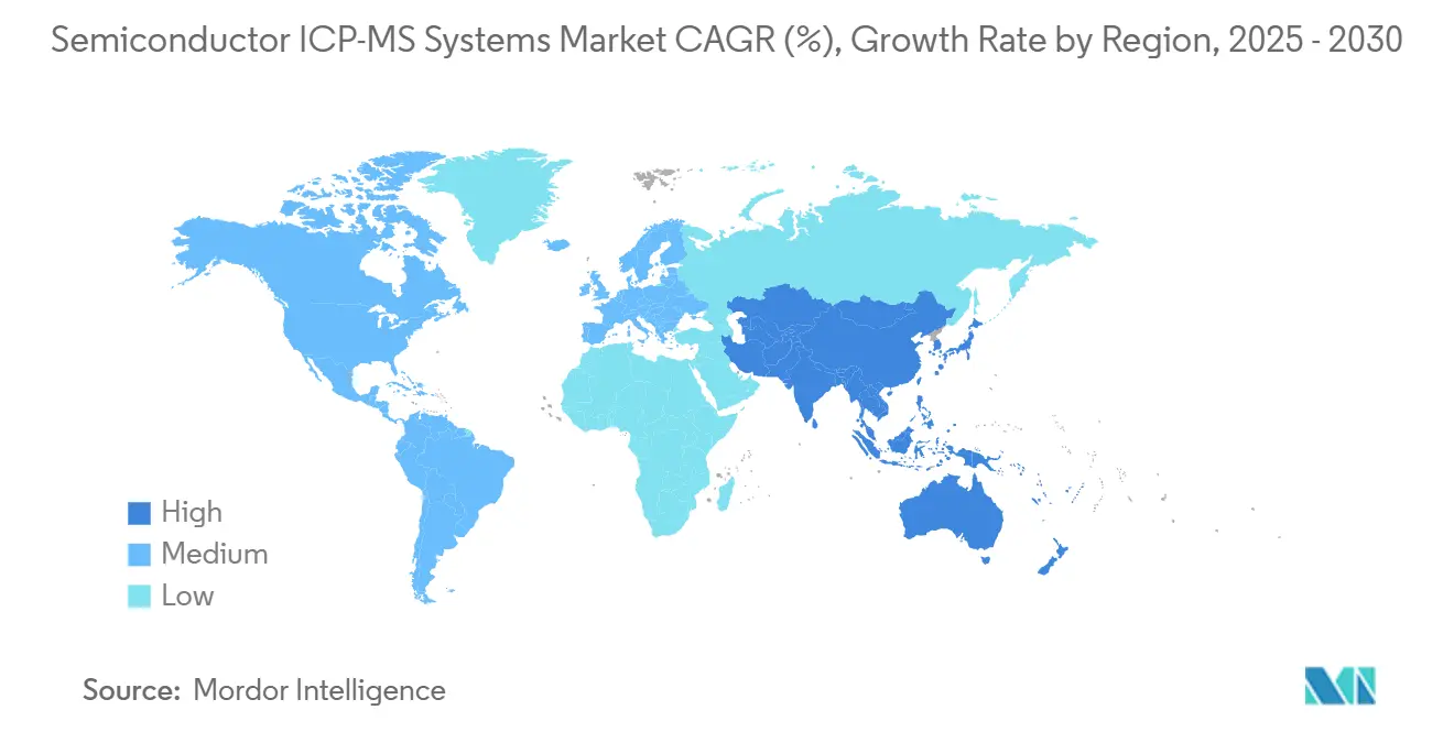
| Fastest Growing Market | Asia Pacific |
| Largest Market | Asia Pacific |
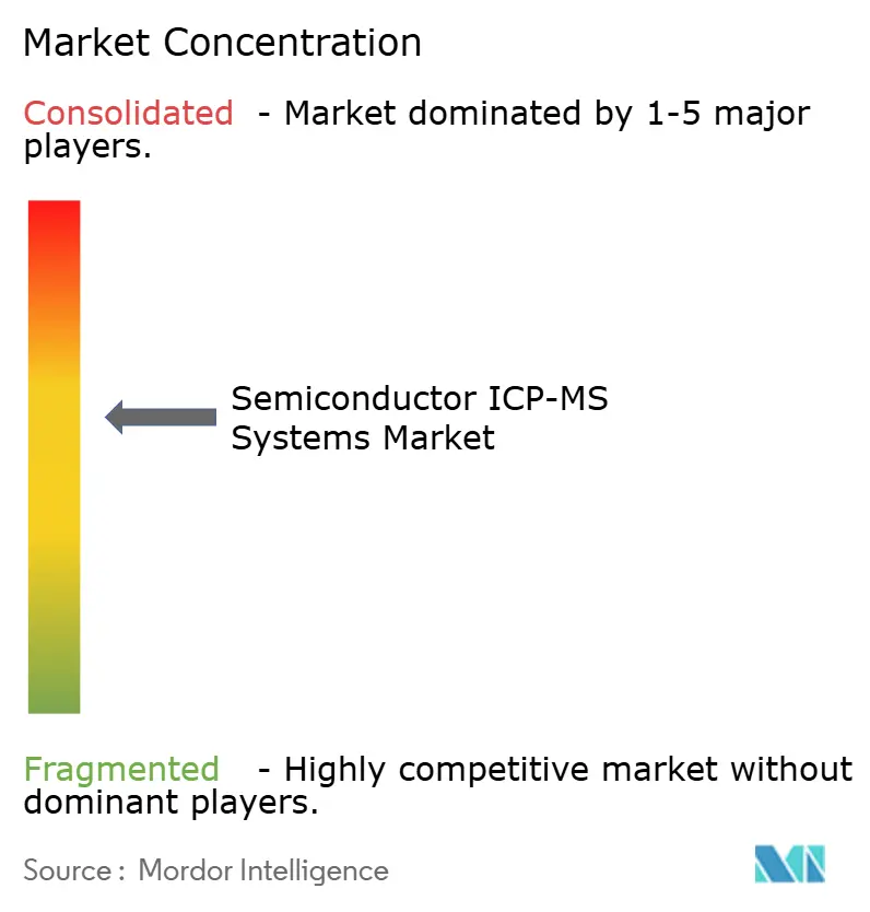
| Market Concentration | Medium |
Major Players *Disclaimer: Major Players sorted in no particular order Image © Mordor Intelligence. Reuse requires attribution under CC BY 4.0. | |
Semiconductor ICP-MS Systems Market Analysis by Mordor Intelligence
The semiconductor ICP-MS systems market size was USD 196.92 million in 2025 and is projected to reach USD 252.76 million by 2030, growing at a 5.12% CAGR over the forecast period. This steady momentum reflects the relentless scaling of the chip industry, where sub-5 nm nodes, extreme-ultraviolet lithography, and atomic-layer deposition all require metal-contamination detection at parts-per-trillion thresholds. Continuous fab investments, rising 3D packaging adoption, and widening trace-metal specifications continue to drive the expansion of the semiconductor ICP-MS systems market, despite capital-intensive entry barriers. The Asia Pacific remains the center of gravity because China, Taiwan, and South Korea each invest tens of billions of dollars in new fabs that require advanced analytical infrastructure. Meanwhile, incremental innovations such as autonomous contamination-prediction software and laser-ablation interfaces open up new spaces for differentiation, even as supply-chain risks surrounding ultra-high-purity argon and skilled metrology labor temper near-term acceleration.
Key Report Takeaways
- By product type, single-quadrupole instruments led the semiconductor ICP-MS systems market with a 48.7% revenue share in 2024, while time-of-flight platforms are projected to advance at a 6.5% CAGR through 2030.
- By application, trace-metal analysis accounted for 41.8% of the semiconductor ICP-MS systems market share in 2024, whereas thin-film thickness measurement is poised to grow at the fastest 6.6% CAGR from 2024 to 2030.
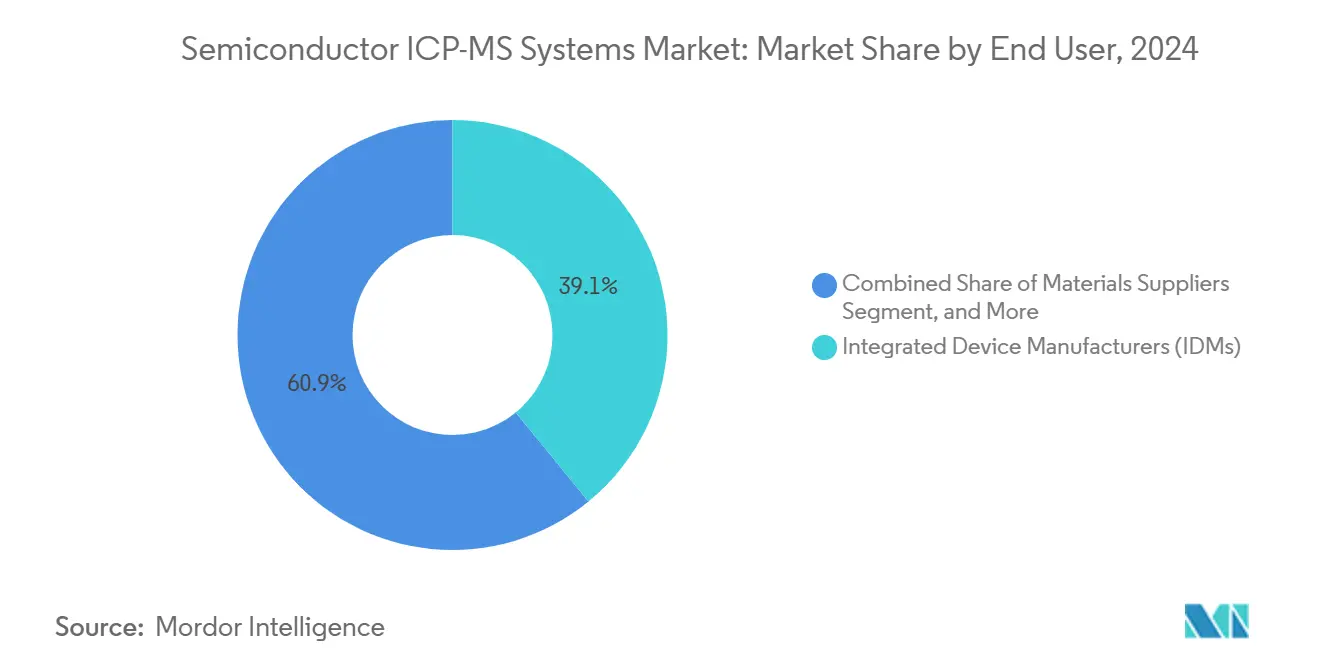
- By end user, integrated-device manufacturers held 39.1% of the demand in 2024 for semiconductor ICP-MS systems; outsourced assembly and test providers are projected to show the highest 7.01% CAGR outlook to 2030.
- By sampling interface, solution nebulization retained a 58.02% share of the semiconductor ICP-MS systems market in 2024; however, laser-ablation adoption is expected to accelerate at a 6.31% CAGR through 2030.
- By geography, the Asia Pacific captured 47.31% of the semiconductor ICP-MS systems market revenue in 2024 and is forecasted to grow at a 6.32% CAGR, outpacing all other regions.
Global Semiconductor ICP-MS Systems Market Trends and Insights
Drivers Impact Analysis*
| Driver | (~) % Impact on CAGR Forecast | Geographic Relevance | Impact Timeline |
|---|---|---|---|
| Intensifying demand for ultra-high-purity process control | +1.2% | Global advanced fabs | Medium term (2-4 years) |
| Proliferation of sub-5 nm semiconductor nodes | +1.1% | Asia Pacific and North America | Long term (≥ 4 years) |
| Expansion of 3D packaging and heterogeneous integration | +0.9% | Global, led by mobile and HPC | Medium term (2-4 years) |
| Growing fab investments in East Asia | +0.8% | China, Taiwan, South Korea | Short term (≤ 2 years) |
| Transition toward gate-all-around transistors | +0.7% | Leading-edge fabs | Long term (≥ 4 years) |
| Increasing adoption of autonomous fab-optimization software | +0.5% | Developed-market fabs | Medium term (2-4 years) |
| Source: Mordor Intelligence | |||
Intensifying Demand for Ultra-High-Purity Process Control
Extreme-ultraviolet lithography and atomic-layer deposition push contamination limits below 10¹⁰ atoms/cm³, making high-resolution ICP-MS indispensable for detecting copper, iron, and nickel at parts-per-trillion levels. TSMC reported more than 15% yield improvement after tightening metallic-impurity control at 3 nm lines.[1]Taiwan Semiconductor Manufacturing Co., “2024 Annual Report,” TSMC.com Moving from 200 mm to 300 mm wafers magnifies the surface area and thus increases the contamination risk, while 3D chiplet integration introduces new metal interfaces that require continuous surveillance. These technical shifts directly lift demand across the semiconductor ICP-MS systems market.
Proliferation of Sub-5 nm Semiconductor Nodes
Device geometries below 5 nm mean that a single stray metal atom can short a transistor; therefore, Samsung’s 3 nm gate-all-around process specifies contamination ceilings of under 1 × 10⁹ atoms/cm².[2]Samsung Electronics, “3 nm Gate-All-Around Production Ramp,” Samsung.com Intel’s USD 20 billion Ohio fab is earmarked USD 500 million solely for advanced metrology, including ICP-MS platforms. The economic penalty of a contamination event at these nodes can exceed USD 10 million per incident, solidifying ICP-MS as a non-negotiable investment across the semiconductor industry.
Expansion of 3D Packaging and Heterogeneous Integration
Through-silicon vias and wafer-level stacking combine dissimilar materials, bypassing traditional clean-room defenses and increasing the complexity of multi-element contamination. Depth-resolved laser-ablation ICP-MS enables engineers to map metal profiles without destroying samples, a feature that shortens failure-analysis cycles. Packaging houses report that early 3D lines are losing more than 20% of their yield due to embedded metallic defects, making rapid in-line monitoring critical for profitability.
Growing Fab Investments in East Asia
Semiconductor outlays exceeded USD 150 billion across China, Taiwan, and South Korea in 2024, with China alone committing USD 47 billion to new fabs.[3]China Daily Staff, “Beijing Increases Semiconductor Build-Out,” Chinadaily.com.cn Every modern fab orders multiple ICP-MS lines for incoming chemicals, wafer surface checks, and waste acid surveillance. Local subsidies in China allocate explicit budgets for contamination-control equipment, thereby amplifying regional demand for semiconductor ICP-MS systems.
Restraints Impact Analysis*
| Restraint | (~) % Impact on CAGR Forecast | Geographic Relevance | Impact Timeline |
|---|---|---|---|
| High capital cost of high-resolution ICP-MS platforms | -0.8% | Global, smaller fabs hit hardest | Short term (≤ 2 years) |
| Scarcity of semiconductor-grade argon supply | -0.6% | Acute in Europe and North America | Medium term (2-4 years) |
| Stringent waste-acid disposal regulations | -0.4% | Developed markets | Long term (≥ 4 years) |
| Limited availability of qualified metrology engineers | -0.5% | Fast-growing Asian hubs | Long term (≥ 4 years) |
| Source: Mordor Intelligence | |||
High Capital Cost of High-Resolution ICP-MS Platforms
A cutting-edge semiconductor-qualified ICP-MS package exceeds USD 1.5 million, and the total cost of ownership doubles once consumables, service, and clean-room retrofits are factored in. For smaller fabs, the outlay can equal 20% of an entire metrology-equipment budget, triggering procurement deferrals or leasing models that slow outright unit shipments across the semiconductor ICP-MS systems market.
Scarcity of Semiconductor-Grade Argon Supply
Ultra-pure argon demand outstrips supply following geopolitical disruptions to key Ukrainian and Russian gas-separation plants, which have tightened spot prices and elongated lead times. Purity shortfalls force some European fabs to idle ICP-MS runs or downgrade detection limits, constraining throughput and delaying capacity expansions.
*Our forecasts treat driver/restraint impacts as directional, not additive. The impact forecasts reflect baseline growth, mix effects, and variable interactions.
Segment Analysis
By Product Type: Time-of-Flight Systems Drive Multi-Element Capabilities
Single-quadrupole instruments accounted for 48.7% of 2024 revenue, underscoring their cost efficiency for routine incoming material screening. However, time-of-flight configurations are projected to grow at a 6.5% CAGR through 2030, as simultaneous full-spectrum acquisition enables the pinpointing of complex contamination fingerprints in seconds, a must for 3D chip architectures.
Multicollector and high-resolution models address narrower niche, such as isotope-ratio studies and spectral-interference suppression, respectively. The semiconductor ICP-MS systems market size for time-of-flight platforms is therefore widening faster than any rival modality, propelled by SEMI method-validation standards that favor multi-element throughput. Supplier roadmaps now bundle TOF engines with automated sample-exchange robots, trimming labor overhead in high-volume fabs. As contamination-source tracing becomes more data-centric, TOF systems’ database-ready spectra make them integral to closed-loop yield engineering suites. Growing patent activity around orthogonal-acceleration TOF ion optics further cements their long-run relevance in the semiconductor ICP-MS systems market.


By Application: Thin-Film Metrology Emerges as Growth Leader
Trace-metal analysis dominated with a 41.8% share during 2024 because every fab qualifies chemicals, water, and airborne molecular contamination by default. Yet thin-film thickness measurement is accelerating at a 6.6% CAGR as gate-all-around transistors and wafer-level stacking demand depth-resolved metal mapping that optical tools cannot deliver. The semiconductor ICP-MS systems market size for thin-film metrology is therefore expanding as memory and logic players turn to laser-ablation ICP-MS to profile diffusion-barrier layers down to single-nanometer precision.
Collision-cell chemistry enhancements suppress silicon and tungsten interferences, enabling repeatable film-composition checks during high-mix production. Vendors now offer turnkey thin-film workflows calibrated to SEMI MS-0110, shortening customer method-validation time. Between 2025 and 2030, thin-film metrology spending is expected to increasingly outpace bulk trace-metal budgets, underscoring its emergence as the growth engine within the broader semiconductor ICP-MS systems market.
By End User: OSAT Providers Show Strongest Expansion
Integrated-device manufacturers led demand at 39.1% in 2024, reflecting scale advantages and centralized labs that multiplex instruments across global fabs. Pure-play foundries ranked second because their diverse customer process flows elevate the complexity of contamination control. Yet outsourced semiconductor assembly and test providers exhibit the sharpest 7.01% CAGR as fabless design houses shift more 3D packaging tasks downstream.
The semiconductor ICP-MS systems market share for OSATs will therefore widen throughout the decade, especially in the Asia Pacific, where proximity to major packaging hubs lowers service turnaround time. Materials suppliers also purchase instruments to verify purity against customer-specified inbound specifications, while research institutions procure high-resolution variants for developing failure-analysis methods. Training partnerships between tool vendors and polytechnic institutes aim to narrow the metrology-engineer shortage that restrains faster adoption.
By Sampling Interface: Laser Ablation Gains Traction for Direct Analysis
Solution nebulization maintained a 58.02% share in 2024, favored for high-throughput liquid analysis where dilution mitigates matrix suppression. Nonetheless, laser ablation is growing at a 6.31% CAGR because it eliminates sample preparation and achieves micron-scale spatial resolution, which is vital for defect localization.
The semiconductor ICP-MS systems market size allocated to laser-ablation bundles is expected to expand as automated stages reduce analysis time and ablation cells integrate contamination-free gas manifolds. Hybrid platforms that allow both solution and solid modes on a single chassis attract IDMs seeking versatility without doubling floor space. Meanwhile, direct solid-sampling workflows have gained SEMI validation for through-silicon via characterization, accelerating their acceptance in advanced packaging lines.
Geography Analysis
The Asia Pacific maintained a 47.31% revenue share in 2024 and is expected to grow at a 6.32% CAGR through 2030, thanks to significant fab build-outs across China, Taiwan, and South Korea. China’s USD 47 billion 2024 semiconductor stimulus earmarks ICP-MS grants, while TSMC’s four new 3 nm fabs in Taiwan will collectively invest more than USD 200 million in contamination-control equipment. South Korean memory leaders are likewise scaling 3D NAND and DRAM nodes that tighten trace-metal limits. Proximity advantages grant regional vendors faster service response, yet Western OEMs still dominate high-resolution shipments, so strategic partnerships emerge to blend technology leadership with local support.
North America ranks second, buoyed by Intel’s USD 20 billion Ohio complex and TSMC’s Arizona mega-fab, both of which demand dozens of semiconductor ICP-MS systems for metrology cells. Federal CHIPS Act subsidies include explicit allocations for contamination-control tools, anchoring long-term domestic demand. University-industry consortia also leverage national lab infrastructure to refine next-gen ICP-MS methods, further strengthening the regional ecosystem.
Europe focuses on automotive and industrial semiconductors, with German power-chip producers setting stringent metal-impurity caps to meet functional-safety standards. The Netherlands’ EUV supply chain sparks niche requirements for high-purity process chemical analysis near ASML’s headquarters. Environmental compliance drives interest in waste-acid recycling modules integrated with ICP-MS exhaust lines, shaping procurement criteria unique to European buyers. While market size lags Asia, specialized application depth secures steady tool refresh cycles across the continent.

Competitive Landscape
The semiconductor ICP-MS systems market is moderately consolidated. Agilent Technologies, Thermo Fisher Scientific, and PerkinElmer collectively control about 60% of global revenue, leveraging decades-long semiconductor relationships, differentiated collision-cell IP, and broad service footprints.[4]Agilent Technologies, “ICP-MS for Semiconductor Manufacturing,” Agilent.com Each firm now embeds AI agents into instrument software that translates ion-count drifts into contamination-risk dashboards, adding stickiness to installed bases. Agilent’s 2024 acquisition of Resolution Systems augments its clean-room-compatible auto-sampler line, while Thermo Fisher’s iCAP TQ launch improves matrix tolerance by 50% and pushes detection limits below 0.1 ppt.
Niche manufacturers, including Nu Instruments and Analytik Jena, carve out high-resolution or multi-collector segments where isotope-ratio accuracy takes precedence over throughput. Software-centric entrants build cloud platforms that ingest real-time ICP-MS streams and other fab sensors to forecast yield dips, challenging traditional OEMs to move beyond hardware differentiation. Patent filings related to automated sample preparation and inline laser-ablation cells increased by 40% in 2024, indicating a shift toward autonomous contamination control ecosystems.
Service providers also capitalize on capital-cost barriers by offering pay-per-sample or subscription-based contamination analysis, particularly attractive to do-it-all OSATs. Vendor financing programs and metrology-equipment-as-a-service packages further democratize access, yet may compress margins if hardware commoditizes faster than software upsells.
Semiconductor ICP-MS Systems Industry Leaders
Agilent Technologies Inc.
Thermo Fisher Scientific Inc.
PerkinElmer Inc.
Shimadzu Corporation
Analytik Jena GmbH
- *Disclaimer: Major Players sorted in no particular order

Recent Industry Developments
- January 2025: Thermo Fisher Scientific began shipping its semiconductor-tuned iCAP TQ ICP-MS, achieving automated sample prep that halves analysis time and reaches sub-0.1 ppt detection limits.
- October 2024: TSMC unveiled a USD 65 billion 2025 capital spending plan, allocating USD 3.2 billion to metrology upgrades that include ICP-MS fleets across its global fabs.
- September 2024: Analytik Jena has earned ISO 17025 accreditation for its Shanghai semiconductor testing laboratory, expanding its third-party contamination services.
- August 2024: Agilent Technologies finalized the USD 180 million purchase of Resolution Systems, adding robotic sample-prep and mini-enclosure platforms to its semiconductor portfolio.


Global Semiconductor ICP-MS Systems Market Report Scope
| Single Quadrupole ICP-MS |
| Multicollector ICP-MS |
| High-Resolution ICP-MS |
| Time-of-Flight ICP-MS |
| Trace Metal Analysis |
| Contamination Monitoring |
| Failure Analysis |
| Thin-Film Thickness Measurement |
| Integrated Device Manufacturers (IDMs) |
| Pure-Play Foundries |
| Outsourced Semiconductor Assembly and Test (OSAT) |
| Materials Suppliers |
| Research Institutions |
| Other End Users |
| Solution Nebulization |
| Direct Solid Sampling |
| Laser Ablation |
| North America | United States |
| Canada | |
| Mexico | |
| South America | Brazil |
| Argentina | |
| Rest of South America | |
| Europe | Germany |
| United Kingdom | |
| France | |
| Italy | |
| Spain | |
| Rest of Europe | |
| Asia Pacific | China |
| Japan | |
| India | |
| South Korea | |
| South-East Asia | |
| Rest of Asia Pacific | |
| Middle East | Saudi Arabia |
| United Arab Emirates | |
| Turkey | |
| Rest of Middle East | |
| Africa | South Africa |
| Nigeria | |
| Rest of Africa |
| By Product Type | Single Quadrupole ICP-MS | |
| Multicollector ICP-MS | ||
| High-Resolution ICP-MS | ||
| Time-of-Flight ICP-MS | ||
| By Application | Trace Metal Analysis | |
| Contamination Monitoring | ||
| Failure Analysis | ||
| Thin-Film Thickness Measurement | ||
| By End User | Integrated Device Manufacturers (IDMs) | |
| Pure-Play Foundries | ||
| Outsourced Semiconductor Assembly and Test (OSAT) | ||
| Materials Suppliers | ||
| Research Institutions | ||
| Other End Users | ||
| By Sampling Interface | Solution Nebulization | |
| Direct Solid Sampling | ||
| Laser Ablation | ||
| By Geography | North America | United States |
| Canada | ||
| Mexico | ||
| South America | Brazil | |
| Argentina | ||
| Rest of South America | ||
| Europe | Germany | |
| United Kingdom | ||
| France | ||
| Italy | ||
| Spain | ||
| Rest of Europe | ||
| Asia Pacific | China | |
| Japan | ||
| India | ||
| South Korea | ||
| South-East Asia | ||
| Rest of Asia Pacific | ||
| Middle East | Saudi Arabia | |
| United Arab Emirates | ||
| Turkey | ||
| Rest of Middle East | ||
| Africa | South Africa | |
| Nigeria | ||
| Rest of Africa | ||


Key Questions Answered in the Report
How large is the semiconductor ICP-MS systems market in 2025?
It is valued at USD 196.92 million and is projected to reach USD 252.76 million by 2030, reflecting a 5.12% CAGR.
Which region currently leads demand for ICP-MS tools in chip fabs?
Asia Pacific holds 47.31% of revenue thanks to heavy fab construction in China, Taiwan and South Korea.
Which product type is expanding fastest?
Time-of-flight ICP-MS platforms are forecast to grow at a 6.5% CAGR because they deliver rapid multi-element spectra.
Why are outsourced assembly and test providers increasing purchases?
OSAT firms support rising 3D packaging volumes and show the strongest 7.01% CAGR as fabless customers outsource contamination-control tasks.
What supply-chain risk affects ICP-MS operations?
Scarcity of semiconductor-grade argon elevates costs and threatens instrument uptime, particularly in Europe and North America.
How competitive is the vendor landscape?
Moderate consolidation prevails, with the top three suppliers capturing about 60% share yet facing mounting pressure from niche and software-centric entrants.
Page last updated on:


