
Optical Coatings Market Size and Share
Market Overview
| Study Period | 2021 - 2031 |
|---|---|
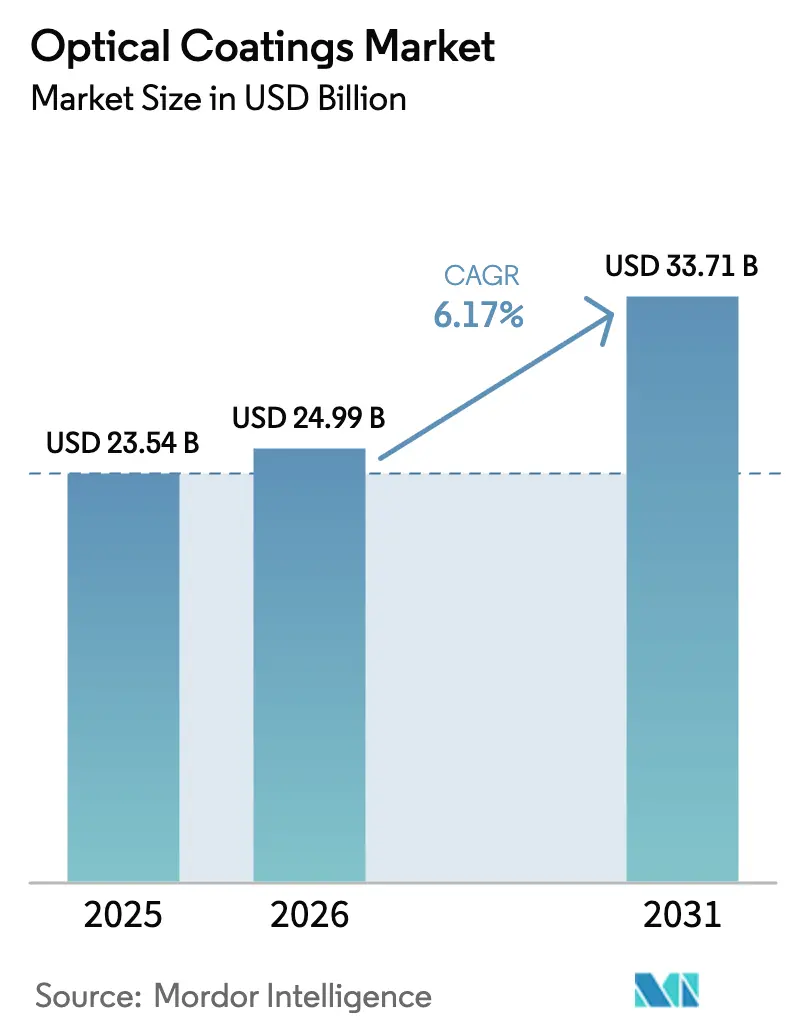
| Market Size (2026) | USD 24.99 Billion |
| Market Size (2031) | USD 33.71 Billion |
| Growth Rate (2026 - 2031) | 6.17 % |
| Fastest Growing Market | Asia Pacific |
| Largest Market | Asia Pacific |
| Market Concentration | Low |
Major Players *Disclaimer: Major Players sorted in no particular order Image © Mordor Intelligence. Reuse requires attribution under CC BY 4.0. | |
Optical Coatings Market Analysis by Mordor Intelligence
The Optical Coatings Market size was valued at USD 23.54 billion in 2025 and is estimated to grow from USD 24.99 billion in 2026 to reach USD 33.71 billion by 2031, at a CAGR of 6.17% during the forecast period (2026-2031). Demand rises as the industry pivots from commodity thin films to engineered stacks that unlock emerging photonics, including bifacial solar modules, metasurface waveguides for augmented-reality headsets, and ultra-low-loss filters for 6G photonic circuits. Anti-reflective coatings hold 37.94% of 2025 revenue, and their 6.46% growth outlook positions them as both the largest and fastest advancing product category. Chemical vapor deposition (CVD) retains a 41.88% share thanks to scalability on Gen 10.5 glass, yet ion-beam sputtering is set to accelerate at 6.81% as aerospace and defense programs demand sub-nanometer precision. Asia-Pacific contributes 34.78% of 2025 sales and expands at 8.11% as China’s display-fab build-out and South Korea’s OLED leadership create regional equipment hubs, while North America and Europe focus on high-value niches such as 6G photonic integrated circuits and automotive LiDAR optics.
Key Report Takeaways
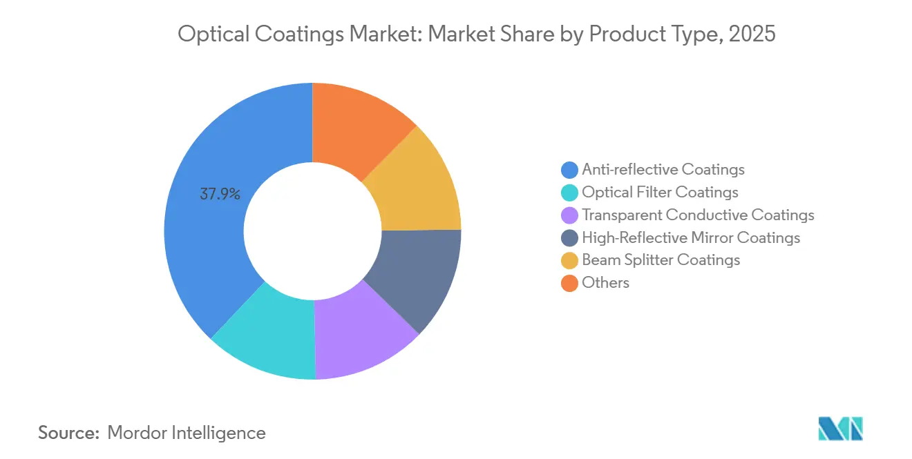
- By product type, anti-reflective coatings led with 37.94% optical coatings market share in 2025; the same segment is forecast to expand at a 6.46% CAGR through 2031.
- By deposition technology, chemical vapor deposition accounted for 41.88% of the optical coatings market size in 2025, whereas ion-beam sputtering records the highest projected CAGR at 6.81% through 2031.
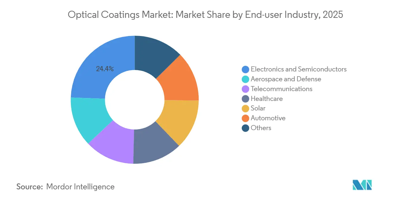
- By end-user, electronics and semiconductors held 24.44% of the 2025 optical coatings market share, while aerospace and defense is forecast to grow fastest at 7.64% to 2031.
- By geography, Asia-Pacific captured 34.78% of revenue in 2025 and is advancing at an 8.11% CAGR, outpacing all other regions.
Note: Market size and forecast figures in this report are generated using Mordor Intelligence’s proprietary estimation framework, updated with the latest available data and insights as of January 2026.
Global Optical Coatings Market Trends and Insights
Drivers Impact Analysis*
| Drivers | (~) % Impact on CAGR Forecast | Geographic Relevance | Impact Timeline |
|---|---|---|---|
| Solar-grade anti-reflective films slash LCOE in bifacial PV modules | +1.2% | Global, with concentration in APAC (China, India) and emerging markets | Medium term (2–4 years) |
| AR/HR meta-coatings enabling AR/VR waveguides for consumer headsets | +0.9% | North America and EU for Research and Development; APAC for volume manufacturing | Short term (≤ 2 years) |
| 6G-ready ultra-low-loss filter stacks for photonic integrated circuits | +0.7% | North America, EU, Japan, South Korea | Long term (≥ 4 years) |
| Military hyperspectral imaging demand for broad-band filter coatings | +1.1% | North America, EU, select Middle East nations | Medium term (2–4 years) |
| Mainstream demand surge from OLED/µLED displays | +1.4% | APAC core (China, South Korea), spill-over to North America and EU | Short term (≤ 2 years) |
| Source: Mordor Intelligence | |||
Solar-Grade Anti-Reflective Films Slash LCOE in Bifacial PV Modules
Bifacial photovoltaic modules equipped with dual-sided anti-reflective stacks now exceed 25% cell efficiency, pushing the levelized cost of energy below USD 0.03 per kilowatt-hour in high-irradiance zones. Tongwei Solar’s 25.5% tunnel-oxide passivated-contact cell, announced in 2025, attributed 0.8 percentage points of gain to optimized front- and rear-surface coatings that minimize reflection from 300 to 1,200 nanometers. Higher output cuts balance-of-system costs, prompting India’s National Institute of Solar Energy to note 18% greater annual yield for bifacial arrays in desert climates. Module manufacturers are internalizing coating steps to secure stack recipes, tightening supply for independent coaters, and favoring players that amortize plasma-enhanced CVD capital across gigawatt-class lines.
AR/HR Meta-Coatings Enabling AR/VR Waveguides for Consumer Headsets
Metasurface waveguides replace bulky multilayer stacks with sub-wavelength nanostructures that slim optical engines below 5 millimeters. Meta Platforms documented a 92%-efficient titanium-dioxide design in 2024[1]Meta Platforms, “Holographic Waveguide Metasurfaces,” nature.com, and Samsung Research followed with a holographic variant in 2025, delivering a 50-degree field of view compatible with eyeglasses. Brands that secure meta-coating intellectual property and align with ion-beam sputtering specialists will control forthcoming consumer-electronics bill of materials, whereas legacy AR vendors face obsolescence unless they invest in nano-fabrication capacity.
6G-Ready Ultra-Low-Loss Filter Stacks for Photonic Integrated Circuits
Telecom operators preparing for 6G trials stipulate insertion loss below 0.1 decibel per centimeter on silicon-nitride waveguides, a target that traditional sputtering fails to meet. Nokia Bell Labs validated coherent transmission at 300 gigahertz using such coatings in 2025, while Ericsson highlighted ±2-nanometer stack-thickness uniformity as the bottleneck for terahertz-band filters. Ion-beam sputtering and ALD deliver the precision but entail capital-intensive, low-throughput tools, igniting regional races; Japan’s AIST and South Korea’s ETRI both aim for 10-wafer-per-hour ALD lines by 2027.
Military Hyperspectral Imaging Demand for Broad-Band Filter Coatings
Defense programs specify coatings that pass narrow spectral bands across 400–2,500 nanometers with out-of-band rejection above 10⁴. The US Navy’s 2024 SBIR call required salt-fog-resistant filters enduring -40 to 70 °C cycles[2]U.S. Navy, “SBIR Topic N241-105,” navy.mil. Army Research Laboratory tests in 2025 showed ion-beam-sputtered coatings on germanium remaining stable after 500 thermal cycles, whereas plasma-sputtered versions drifted 12 nanometers. NATO’s 2024 standard fixed ±1-nanometer uniformity across 100-millimeter apertures, effectively excluding CVD. Vendors that balance high-value, low-volume defense demand with lower-spec commercial sensors will defend margins.
Restraints Impact Analysis*
| Restraints | (~) % Impact on CAGR Forecast | Geographic Relevance | Impact Timeline |
|---|---|---|---|
| Indium-tin-oxide supply vulnerability | -0.8% | Global, acute in North America and EU due to import dependence | Short term (≤ 2 years) |
| Stricter PFAS bans hitting fluoride-based hard coats | -0.5% | EU, North America; limited impact in APAC | Medium term (2–4 years) |
| CAPEX intensity of atomic-layer deposition lines | -0.6% | Global, most acute in regions with limited fab subsidies | Long term (≥ 4 years) |
| Source: Mordor Intelligence | |||
Indium-Tin-Oxide Supply Vulnerability
China controls 60% of refined indium, and the United States imported 100% of its need in 2024 according to the US Geological Survey. A 35% price jump in 2023–2024 reflects tightened export quotas, while recycling captures less than 15% of scrap. Display makers fund alternatives such as graphene and silver nanowires, yet none match ITO’s conductivity-transparency balance at mass scale. Samsung Display allocated USD 120 million to ITO-free research, but commercial release is unlikely before 2028, leaving coaters exposed to raw-material inflation.
Stricter PFAS Bans Hitting Fluoride-Based Hard Coats
The US Environmental Protection Agency labelled select PFAS hazardous substances in April 2024, and the European Chemicals Agency added four to its REACH candidate list the same year. Replacements such as siloxanes exhibit 30% higher Taber-wear indices, lowering smartphone-screen durability. Corning is qualifying PFAS-free formulations for Gorilla Glass but expects 12–18 months of additional customer testing, disproportionately burdening small coating houses.
*Our forecasts treat driver/restraint impacts as directional, not additive. The impact forecasts reflect baseline growth, mix effects, and variable interactions.
Segment Analysis
By Product Type: Anti-Reflective Coatings Lead Across Solar and Display
Anti-reflective coatings commanded 37.94% of revenue in 2025, and the segment is projected to expand at a 6.46% CAGR through 2031. Dual-sided stacks on bifacial solar glass and low-reflectance layers on OLED panels account for nearly two-thirds of consumption. Transparent conductive coatings, hindered by indium constraints, still post mid-single-digit growth as microLED head-up displays and wearables mature. High-reflective mirror coatings remain specialized for laser systems, while beam splitters support machine-vision cameras in industrial automation. Specialty filters servicing biophotonics and quantum optics sustain gross margins above 50%.
Momentum is shifting from broadband AR stacks toward wavelength-selective metasurface films that reduce reflection below 0.5% with sub-10-nanometer thickness. Samsung Research unveiled a flexible variant in 2024, and Tokyo Electron is scaling nano-imprint tools that pattern 300-millimeter wafers at 20-per-hour throughput. Coaters tied solely to CVD or sputtering lack sub-50-nanometer pattern capabilities and risk commoditization as Asian fabs internalize multilayer recipes.



By Deposition Technology: CVD Dominates, Ion-Beam Sputtering Gains in Precision Niches
CVD generated 41.88% of 2025 revenue, underpinned by uniform deposition across 3-meter glass for OLED encapsulation. Plasma-enhanced CVD achieves ±2% thickness control, serving Gen 10.5 lines at BOE and LG Display. Ion-beam sputtering, while capturing only 14% of sales, delivers sub-nanometer roughness and is projected to expand at 6.81% through 2031, led by defense lasers and hyperspectral imaging. Plasma sputtering fills automotive and consumer-electronics needs where speed outweighs atomic-scale precision, whereas ALD remains indispensable for flexible OLED barriers and high-aspect photonics structures.
Sub-wavelength structured surfaces threaten conventional stacks by eliminating vacuum films. Canon’s 2025 300-millimeter nano-imprint tool achieves 10-wafer-per-hour throughput. If metasurfaces displace layers in foldable screens and AR headsets, value will migrate from deposition to lithography-etch toolmakers, pressing coaters to diversify or license metasurface IP.
By End-User Industry: Electronics Lead, Aerospace Grows Fastest
Electronics and semiconductors consumed 24.44% of optical coatings in 2025, driven by OLED, smartphone cameras, and laptop displays. Samsung Display and LG Display alone processed 18,000 metric tons of ITO in 2024, equal to 40% of global indium refining. Aerospace and defense will outpace all sectors at a 7.64% CAGR as hyperspectral imaging and directed-energy optics demand coatings with 10⁵ out-of-band rejection. Solar contributes through bifacial modules, while automotive shifts from anti-glare cabin displays toward LiDAR and AR windshields requiring low-loss coatings at 905 and 1,550 nanometers.
Automotive advanced driver-assistance systems integrate eight cameras and four LiDAR sensors per vehicle, each calling for multilayer AR stacks tuned to infrared bands. Continental’s 2024 roadmap and Bosch’s 2025 partnership with Zeiss target less than 0.5% reflection for all-weather range. Healthcare optics and telecom photonics are advancing, with Olympus and Karl Storz applying ALD anti-fog layers on endoscopes, while Nokia concentrates on 6G-ready filter stacks.
Geography Analysis
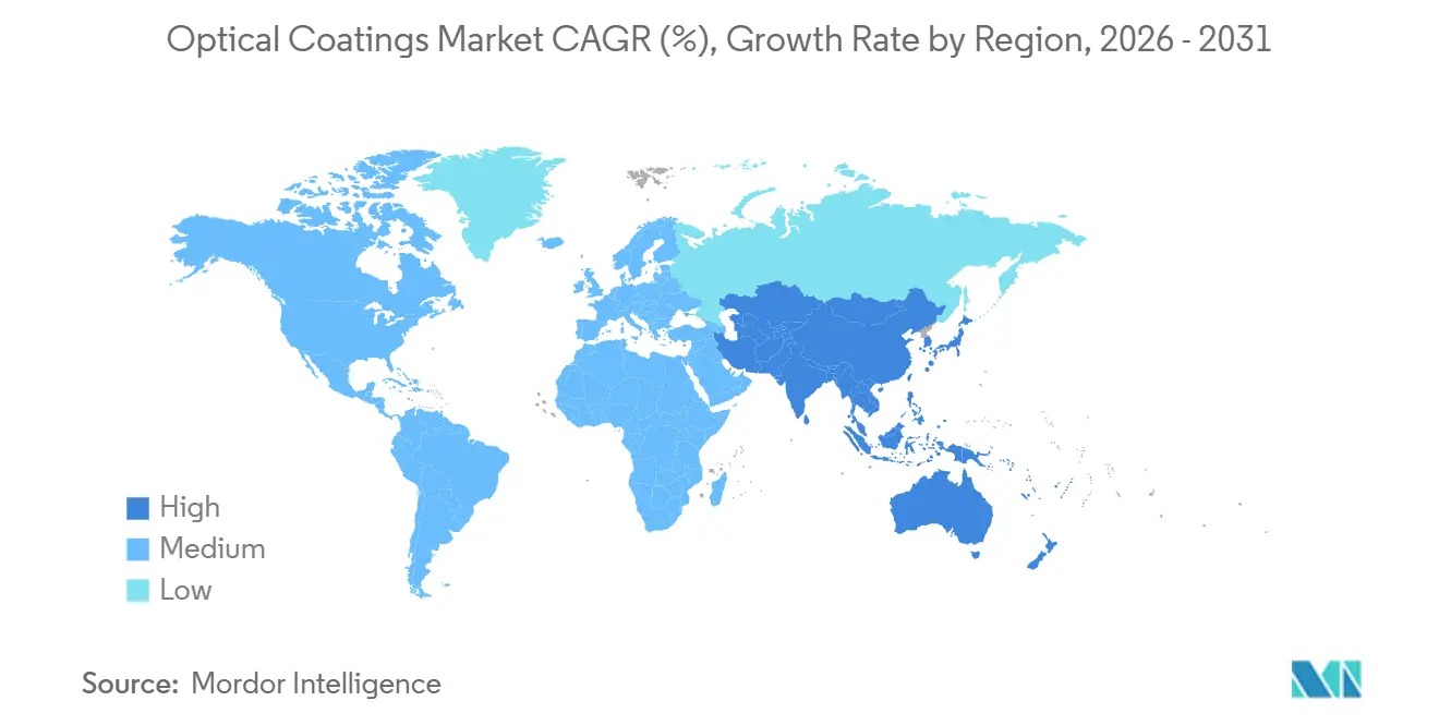
Asia-Pacific held 34.78% of 2025 revenue and is advancing at an 8.11% CAGR to 2031, adding more than USD 3 billion to the optical coatings market size during the period. China, South Korea, and Japan anchor regional dominance through OLED production, solar module assembly, and precision metrology toolmaking. India’s National Institute of Solar Energy reported that locally coated bifacial glass trims module costs by USD 0.02 per watt, stimulating domestic coating-line investment. Southeast Asia emerges as a secondary hub as brands diversify away from China, although limited semiconductor infrastructure restrains photonic-grade growth.
Military optics and photonic integrated circuits propel North America's optical coatings market growth. The US Department of Defense allocated USD 1.8 billion in 2024 for electro-optical and infrared systems, driving demand for ion-beam coatings that survive harsh environments. Materion and Coherent leverage classified-program credentials to secure contracts, while Canada’s photonics cluster leverages National Research Council grants for coating development. Mexico attracts automotive-coating projects such as PPG’s USD 45 million expansion in Tlaxcala, serving Ford and GM plants.
Europe accounts for a significant share of the global optical coatings market as Germany, France, and the United Kingdom dominate automotive and industrial optics. Schott and Zeiss supply PFAS-free conformal layers following the EU’s tightened chemical regulations. The Middle East and Africa are witnessing rising demand for optical coatings due to solar mega-projects like Saudi Arabia’s NEOM, which incorporates 5 gigawatts of bifacial modules requiring dual-side coatings.

Value Chain Analysis
The optical coatings value chain begins with high-purity inputs (for example, indium-tin-oxide for transparent conductive layers, and oxide or fluoride targets and precursors such as hafnium oxide and ytterbium fluoride for advanced stacks), then moves through substrate preparation (glass, polymers, wafers), deposition, metrology, and downstream integration into optics, displays, sensors, and modules. Deposition is carried out via CVD, ion-beam sputtering, plasma sputtering, e-beam evaporation, and ALD, and process capability depends heavily on contamination control and on qualification against quality frameworks such as ISO 9001, AS9100 (aerospace), and IATF 16949 (automotive).
Equipment access and regulated chemistry supply are key bottlenecks. Advanced ion-beam sputtering and ALD platforms can also have long tool lead times, which limits capacity additions for sub-nanometer-precision coatings used in defense optics and photonic integrated circuits. Engineered coated components can face extended fulfillment cycles as well, given tighter metrology and reliability testing requirements. On the materials side, the market remains exposed to ITO availability and pricing, and in 2026 South Korea's Ministry of Environment timeline for the K-REACH supply-shortage chemical substances special registration provision (with the application channel announced to close on 30 June 2026) adds compliance friction for exports of certain optical coating liquids. This dynamic supports more secured supplier relationships, safety stock build-ups, and vertical integration by large OEMs.
Competitive Landscape
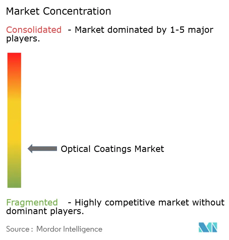
The global optical coatings market is higly fragmented. Vertical integration by display giants BOE, Samsung Display, and LG Display siphons margin from merchant suppliers. Technology adoption is decisive. Firms that master ion-beam and ALD for aerospace yet maintain CVD throughput for consumer electronics hold pricing power, whereas single-technology specialists face commoditization. Regulatory leadership offers another edge: European suppliers achieving PFAS-free coatings ahead of 2027 REACH deadlines secure automotive contracts, while laggards risk withdrawals. Mergers and acquisitions are expected as larger players acquire process IP and customer bases, leaving niche specialists and captive lines to dominate by 2030.
Optical Coatings Industry Leaders
Zeiss International
Materion Corporation
PPG Industries Inc.
DuPont
VIAVI Solutions Inc.
- *Disclaimer: Major Players sorted in no particular order

Market Opportunities and Future Outlook
Wafer-level and metasurface-enabled optics are creating whitespace for coaters and toolmakers that can deliver uniformity and defect control at semiconductor-like standards. Fraunhofer IST has emphasized an industrial production approach for precision optical coatings (EOSS) that uses simultaneous double-sided deposition, which points to manufacturing architecture changes aimed at higher throughput and tighter-uniformity requirements for AR waveguides, photonic integrated circuits, and high-end sensors. At the same time, investments in AR optics manufacturing, including a new 12-inch AR optical wafer fab ramp in Shanghai by Goertek OmniLight Optical Technology with diffractive waveguides and nanoimprint processes, highlight demand for coating stacks that work within wafer-based process flows. This supports opportunities for ALD and ion-beam sputtering services, along with targets and precursors and more advanced metrology capabilities.
Large-aperture and space or astronomy optics also offer a monetizable niche where coating equipment capability can differentiate for nonstandard geometries, consistent with VON ARDENNE actions around 2026 involving the OPTA X300 tool in Dresden and the SKYVA2000 system for large curved mirrors up to 2 meters in diameter. Across end markets, PFAS-related reformulation work referenced in the report context reinforces demand for PFAS-free hard coats with durable performance for consumer electronics and automotive optics, while throughput economics for high-volume display and solar glass lines remain a gating factor for qualification and scale.
Recent Industry Developments
- May 2026: HEF Photonics USA completed acquisition of Evaporated Coatings, Inc. (ECI), expanding ion-beam sputtering capabilities and coating-system capacity in its US footprint. The acquisition supports defense and aerospace coating programs and increases competitive pressure on smaller coaters that rely on limited toolsets.
- October 2025: ZEISS and LG Chem established a strategic framework to strengthen supply of photopolymer film for automotive holographic windshield display applications. The agreement connects optics and coating know-how with upstream materials sourcing, supporting industrial-scale adoption for next-generation in-vehicle display optics.
- June 2024: Materion Corporation secured a multi-year contract to deliver ion-beam-sputtered coatings for airborne and space hyperspectral sensors. The award reinforces demand for sub-nanometer-precision coatings and highlights the value of qualified suppliers with defense-grade process control and reliability testing.


Research Methodology Framework and Report Scope
Market Definition and Coverage
In this report, the optical coatings market covers thin film coatings applied to optical components and substrates to manage reflection, transmission, and filtering performance across visible, UV, and IR ranges.
Scope exclusions: This sizing excludes bulk optical materials and uncoated optics, and it also excludes coating equipment sales and contract deposition services when they are counted as standalone services.
Segmentation Overview
- By Product Type
- Optical Filter Coatings
- Anti-reflective Coatings
- Transparent Conductive Coatings
- High-Reflective Mirror Coatings
- Beam Splitter Coatings
- Others
- By Deposition Technology
- Chemical Vapor Deposition
- Ion-beam Sputtering
- Plasma Sputtering
- Atomic Layer Deposition
- Sub-wavelength Structured Surfaces
- By End-user Industry
- Aerospace and Defense
- Electronics and Semiconductors
- Telecommunications
- Healthcare
- Solar
- Automotive
- Others
- By Geography
- Asia-Pacific
- China
- Japan
- South Korea
- India
- ASEAN Countries
- Rest of Asia-Pacific
- North America
- United States
- Canada
- Mexico
- Europe
- Germany
- United Kingdom
- France
- Italy
- Spain
- Nordic Countries
- Russia
- Rest of Europe
- South America
- Brazil
- Argentina
- Rest of South America
- Middle-East and Africa
- Saudi Arabia
- South Africa
- Rest of Middle-East and Africa
- Asia-Pacific
Data Sources, Market Sizing, and Validation
Desk Research
Desk research starts with public data that helps us map where optical coatings are used and how fast key end markets are expanding. We rely on sources such as the US International Trade Commission trade statistics, UN Comtrade, and government manufacturing output series to anchor the direction of optical component and substrate flows. When defense and aerospace demand signals are relevant, we also review open defense procurement notices and civil aviation fleet additions published by official bodies.
We then add industry-facing materials like company annual reports, earnings decks, product catalogs, and technical notes to map common coating stacks and where pricing tends to differ by application. Patent databases and peer-reviewed thin film journals are used to confirm which coating types and deposition approaches are scaling, before assumptions are locked. We also use paid subscriptions for company financials and intelligence, plus patent analytics, mainly to keep peer checks consistent across regions. The sources listed here are illustrative, and other public references were used to gather, cross-check, and clarify inputs.
Primary Interviews and Surveys
Primary work is used to test the revenue boundary, plus the pricing and volume assumptions behind typical optical coating orders. We speak with a mix of coating material suppliers, optics component makers, and downstream buyers in electronics, automotive, medical optics, and defense, and we ensure coverage reflects demand hotspots across APAC, EMEA, and the Americas. These conversations help close gaps around yield loss, qualification cycles, and how much coating value is kept in-house versus outsourced, which then tightens the model outputs.
Distribution of primary research fieldwork respondents
| Company type | Respondent position | Region |
|---|---|---|
| Top tier: 27% | CXOs: 19% | APAC: 46% |
| Mid tier: 52% | Functional/Unit leaders: 32% | EMEA: 35% |
| Smaller Players: 21% | Managers: 49% | Americas: 19% |
Market-Sizing & Forecasting
Sizing uses a top-down approach once the demand pool is rebuilt from optical component production and trade movement, then translated into coating value using attach rates and typical coating intensity by end use. To keep it grounded, totals are corroborated with selective bottom-up checks, where a sampled set of supplier revenues, channel conversations, and volume times ASP sanity checks are used to adjust totals when mismatches show up.
Key inputs used in the model include optical component shipment direction by region, the share of coated versus uncoated parts in high-volume uses, average coating price progression by application, deposition capacity utilization and expansion timing, and end market output indicators for electronics, automotive sensing, and medical optics. Where direct volume is not visible, gaps are handled through ranges from primary discussions, followed by conservative mid-point selection and back-testing against historical growth. For forecasting, scenario analysis is used around end market build plans and qualification lead times, and the final path is selected when expert consensus aligns on the most probable volume ramp and ASP change.
Data Validation & Update Cycle
Outputs are checked against independent signals so the model does not drift from real demand, including trade flow direction, major capacity additions, and end market production trends. When outliers appear, the driver assumptions are reopened and the related interviews are re-contacted, so the variance is explained rather than averaged away.
Before sign-off, the work goes through a multi-step analyst review where calculations, unit logic, and currency handling are rechecked, and key assumptions are challenged. Reports refresh annually, and interim updates are made when material events change supply, pricing, or downstream demand. Right before delivery, an analyst performs a fresh pass on the latest public updates so clients receive the most current view.
Mordor Intelligence's Optical Coatings Market Size Compared With Other Published Estimates
Published market sizes for optical coatings can look far apart because the boundary of what is counted is not always the same, and the timing of pricing and currency assumptions can shift totals. Differences also come from how demand is tied to real optical component output versus broader photonics or electronics spending, which can expand the addressable pool.
By tracking deposition capacity utilization, attach rates by end use, and annual currency timing, Mordor Intelligence keeps the optical coatings total aligned to coated optics demand rather than adjacent services and equipment revenue. Some estimates widen the scope into coating tools or include contract deposition revenue as a separate service line, and others rely on aggressive ASP increases without validating them through buyer checks and yield loss realities.
Benchmark comparison
| Source | Market Size | Gaps in Research Methodology |
|---|---|---|
| Mordor Intelligence | USD 24.99 B (2026) | |
| Global Consultancy A | USD 22.05 B (2024) | This estimate uses an earlier base year and a different forecast window, and it can also pull in broader optical coating value tied to general photonics demand, which shifts attach rates and ASP assumptions. |
| Industry Publisher B | USD 10.28 B (2024) | This estimate appears to apply a narrower product boundary and may exclude parts of high-volume coated optics demand, especially where coatings are bundled into component pricing and not counted separately. |
The table shows that the biggest drivers of spread are the year used for sizing and the scope boundary around what is treated as coating revenue. When assumptions are anchored to observable optical component flow and then pressure-tested through supplier and buyer checks, the outcome stays traceable, repeatable, and easier to defend in planning discussions.


Key Questions Answered in the Report
How large is the optical coatings market in 2026?
The optical coatings market size is USD 24.99 billion in 2026, with a forecast to reach USD 33.71 billion by 2031.
Which product segment contributes the most revenue?
Anti-reflective coatings dominate, holding 37.94% of 2025 revenue and projected to expand at a 6.46% CAGR.
Which deposition technology is growing fastest?
Ion-beam sputtering shows the highest growth outlook at 6.81% due to aerospace and defense demand for sub-nanometer precision.
Why is Asia-Pacific outpacing other regions?
Concentrated OLED production, solar module assembly, and semiconductor packaging give Asia-Pacific a 34.78% share and 8.11% CAGR through 2031.
What is the main supply-chain risk for coaters?
Dependence on indium-tin-oxide, with China controlling 60% of refining and the United States importing 100% of its needs, exposes the sector to price spikes and geopolitical risk.
How strict are upcoming PFAS regulations?
The U.S. EPA labeled certain PFAS hazardous in 2024, and the EU plans broad restrictions by 2027, prompting coaters to reformulate hard-coat chemistries.
Page last updated on:


 Your data is secure and never sold or shared.


