
Glass Core Substrate Market Size and Share
Market Overview
| Study Period | 2022 - 2032 |
|---|---|
| Market Size (2027) | USD 1.57 Billion |
| Market Size (2032) | USD 5.07 Billion |
| Growth Rate (2027 - 2032) | 26.45 % |
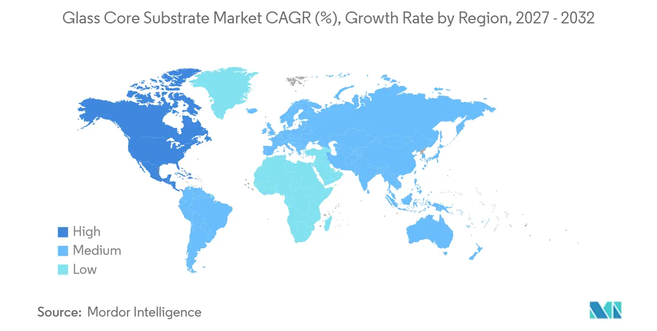
| Fastest Growing Market | North America |
| Largest Market | Asia-Pacific |
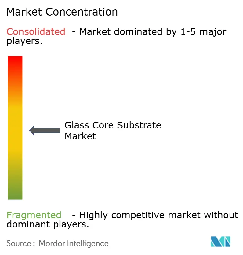
| Market Concentration | Medium |
Major Players *Disclaimer: Major Players sorted in no particular order Image © Mordor Intelligence. Reuse requires attribution under CC BY 4.0. | |
Glass Core Substrate Market Analysis by Mordor Intelligence
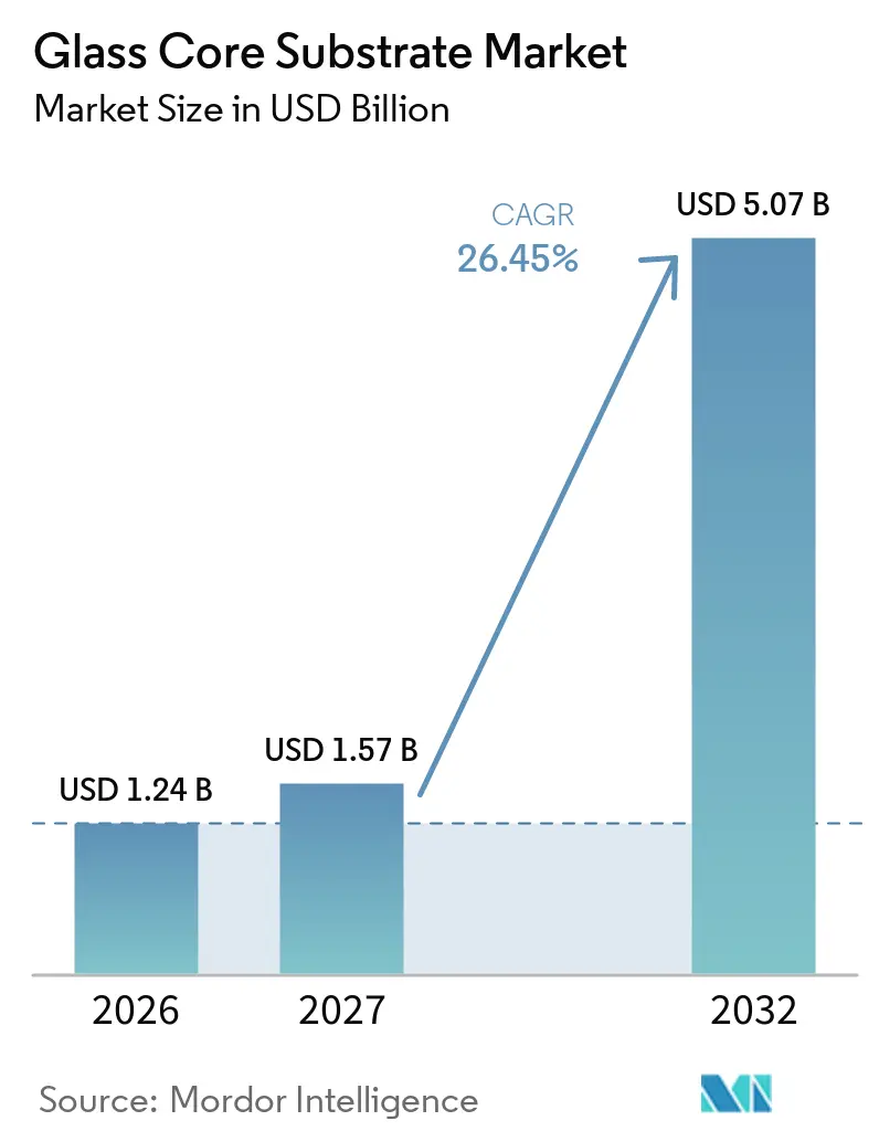
The Glass core substrate market size was valued at USD 1.24 billion in 2026 and is estimated to grow from USD 1.57 billion in 2027 to USD 5.07 billion by 2032, at a CAGR of 26.45% during the forecast period (2027-2032). Growth in the glass core substrate market reflects the need for flatter, dimensionally stable substrates as AI accelerator packages integrate more dies and high-bandwidth memory within larger package footprints, increasing pressure on every layer of the packaging supply chain to maintain precision at scale. Organic cores face increasing warpage and overlay limits as package dimensions rise, making glass a practical option for advanced redistribution layers when designers require closer die placement, reliable alignment, stable package behavior across thermal processing steps, and predictable performance during assembly. Panel processing also offers the glass core substrate market a path toward better material use and lower package costs at scale, as large formats can carry several packages through Through Glass Via (TGV) formation, copper filling, redistribution-layer patterning, and inspection within the same production cycle, reducing the need for repeated setup. Competition depends on access to low-coefficient-of-thermal-expansion glass, production yields, and successful customer qualification, rather than end-user demand alone, as new melting capacity takes time to build and reliability evidence must be developed for each customer application, package design, and operating environment. Commercial timing remains uncertain because TGV process maturity and customer adoption could defer broad production toward 2029 or later. The gap between committed AI demand and qualified supply means that near-term gains depend on yield performance, access to materials, process uniformity across large panels, and the pace of customer approvals. Customer decisions reflect a balance between material performance, equipment readiness, qualification evidence, stable supply, demonstrated manufacturing control, and confidence in long-term process repeatability for high-value packages.
Key Report Takeaways
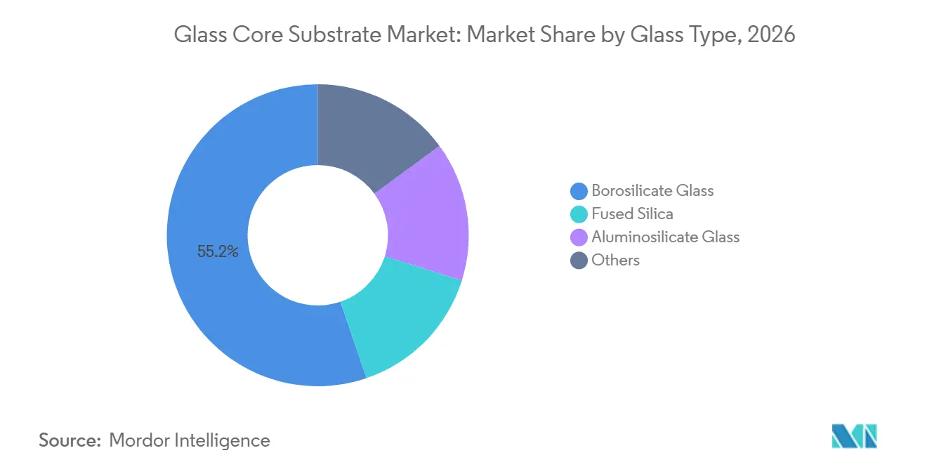
- By glass type, borosilicate glass held 55.23% market share in 2026, while aluminosilicate glass is forecast to grow at a 28.57% CAGR through 2032.
- By substrate format, panel-based glass core substrates held 55.72% market share in 2026 and are forecast to grow at a 27.14% CAGR through 2032.
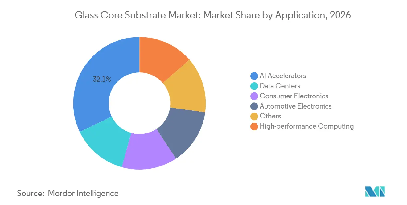
- By application, AI accelerators accounted for 32.11% market share in 2026, while high-performance computing is forecast to expand at a 29.62% CAGR through 2032.
- By geography, Asia-Pacific held 36.88% market share in 2026, while North America is forecast to expand at a 27.94% CAGR through 2032.
Note: Market numbers in this report are based on Mordor Intelligence's proprietary estimation framework, which combines nine months of actuals with Q4 projections for base year 2026.
Global Glass Core Substrate Market Trends and Insights
Drivers Impact Analysis*
| Drivers | (~) % Impact on CAGR Forecast | Geographic Relevance | Impact Timeline |
|---|---|---|---|
| AI and HPC Package Scaling | +9.0% | Global | Short term (≤ 2 years) |
| Organic Substrate Warpage and Overlay Limits | +5.5% | Global, concentrated in APAC packaging centers | Medium term (2-4 years) |
| Panel-Level Packaging Economics | +4.5% | APAC core, spillover to North America | Long term (≥ 4 years) |
| Co-Packaged Optics and High-Speed Interconnect Demand | +3.5% | North America and APAC data center clusters | Long term (≥ 4 years) |
| Glass Material and TGV Process Maturation | +2.5% | Global | Short term (≤ 2 years) |
| Source: Mordor Intelligence | |||
AI and HPC Package Scaling
The glass core substrate market is responding to AI chipmakers designing packages that place multiple compute dies and high-bandwidth memory stacks within a single substrate. These designs require tight flatness and dimensional control that laminated organic cores struggle to deliver at large sizes, particularly when routing density, memory integration, and package area must increase together without reducing manufacturing yield. TSMC stated that advanced packaging contributed 8% of its revenue in 2025 and is expected to exceed 10% in 2026, indicating that more semiconductor value is moving into package architecture. The glass core substrate market benefits because glass can support fine redistribution layers while limiting dimensional movement across a large package. The cost of a Chip on Wafer on Substrate (CoWoS)- packaged wafer has moved closer to that of a 7 nm process node, strengthening the case for alternatives that can support density at a lower cost after qualification. NVIDIA and Broadcom are evaluating glass interposer and glass core roadmaps, connecting substrate development more directly with AI package demand.
Organic Substrate Warpage and Overlay Limits
Organic cores have a mechanical constraint that becomes more apparent as package area grows, because the accumulated effect of material movement becomes harder to correct after redistribution layers and chiplets are placed. Research presented at IEEE ECTC in 2025 found that glass cores exhibited lower warpage and better positional accuracy than organic-core alternatives[1]. This performance supports redistribution layer line and space dimensions below 2 µm, while organic materials become harder to control at the dimensions required by AI chiplets. Organic laminates also expand and contract differently from silicon, so dimensional drift increases as package size rises. That drift forces more conservative design rules and can limit interconnect density in 2.5D architectures. As via pitches move below 50 µm, tighter warpage tolerances could make glass a more viable route to specification compliance for advanced packages.
Panel-Level Packaging Economics
In the glass core substrate market, panel processing is important because its cost advantage comes from scale rather than from glass material properties alone, and because larger formats can spread each process step across a larger usable package area. Traditional 300 mm wafer processing uses 45% of the available area, whereas large-panel processing can use 81%. Suppliers now offer glass in 510 × 515 mm and 550 × 650 mm formats, which enable several packages to move through TGV formation, metallization, redistribution layer patterning, and inspection in a single cycle. This model spreads fixed processing costs across a larger usable area as package sizes increase. The glass core substrate market, therefore, has a cost path that is less dependent on constrained capacity in silicon interposers. SEMI expects adoption to expand after 2028 as several qualification programs progress concurrently.
Co-Packaged Optics and High-Speed Interconnect Demand
Co-packaged optics is a high-value use case for the glass core substrate market because glass can combine electrical and optical functions within a single package, enabling designers to pursue closer photonic integration as data movement requirements increase. Research published in 2026 reported that TGV and redistribution layer structures on glass can reach bandwidths of up to 110 GHz and line densities above 500 lines per mm at a 2 µm line-space configuration. The same work reported waveguide propagation losses as low as 0.034 dB/cm using ion-exchange processing. These properties can support closer integration of photonic and electronic circuits and reduce the need for separate photonic packages. For data centers, lower electrical-to-optical conversion requirements may reduce network switch power demand. AT&S identifies co-packaged optics as a near-term commercial focus for its glass substrate program.
Restraints Impact Analysis*
| Restraints | (~) % Impact on CAGR Forecast | Geographic Relevance | Impact Timeline |
|---|---|---|---|
| High Qualification and Reliability Burden | -5.5% | Global, with heightened impact in North America and Europe for automotive end markets | Long term (≥ 4 years) |
| TGV, Metallization, Dicing Yield Losses, and Handling Complexity | -4.5% | Global, concentrated in APAC manufacturing centers | Short term (≤ 2 years) |
| Fragility, SeWaRe, and Handling Complexity | -3.0% | Global | Short term (≤ 2 years) |
| Source: Mordor Intelligence | |||
High Qualification and Reliability Burden
Within the glass core substrate market, qualification requirements create different adoption paths for each end market, as each customer must assess material behavior, process consistency, and reliability under its own operating conditions. Data center customers focus on package cost, yield, and design cycle speed, so their adoption depends primarily on materials readiness. Automotive customers require thermal cycling, humidity, vibration, and metallization reliability testing, which can extend adoption by 18 to 36 months beyond data center programs. Each supplier must build qualification data for each customer and application because glass is a new core material rather than a minor process change. This increases engineering costs and favors suppliers that can fund dedicated reliability work. Intel's licensing-oriented approach to glass-substrate intellectual property also indicates that commercialization requires sustained investment before broad revenue can be generated.
Through-Glass Via (TGV), Metallization, Dicing Yield Losses, and Handling Complexity
The glass core substrate market still faces technical barriers in through-glass via (TGV) drilling, copper metallization, glass singulation, and handling, as a defect at any stage can reduce yield and make large-panel processing uneconomic. IEEE Electronic Components and Technology Conference (ECTC) research described SeWaRe as backside splitting that occurs when laminated buildup layers reach the singulated edge and stress concentrates around small surface defects. The research found that a pull-back approach can prevent this cracking, but it requires changes to build-up stack design across supplier production flows. Panel-level TGV formation also requires tight etch uniformity across large formats, which makes yield control difficult. A 2025 review described TGV diameters from 20 µm to 150 µm on panels up to 550 × 650 mm, showing the range of processes under development. Work on machine-learning-based overlay correction further indicates that production methods are still being refined to achieve simultaneous accuracy and throughput.
*Our forecasts treat driver/restraint impacts as directional, not additive. The impact forecasts reflect baseline growth, mix effects, and variable interactions.
Segment Analysis
By Glass Type: Established Chemistry Leads, Specialty Grades Accelerate
Borosilicate glass held 55.23% of global revenue in 2026. Its process chemistry is well characterized across semiconductor packaging, and the glass core substrate market has relied on material choices that customers can qualify with greater confidence. Its coefficient of thermal expansion profile also suits a wide range of package-to-printed circuit board (PCB) assembly conditions. SCHOTT and Corning offer several product families in wafer and panel formats, giving early programs access to established material options. Many early customer qualifications use borosilicate because it is available at commercial purity and dimensional specifications. This availability supports demand even when a customer does not require premium material performance, as material selection during early programs is influenced by familiarity, purity, dimensional control, and access to established process data. The leading position, therefore, reflects supply readiness as much as it reflects technical fit.
Aluminosilicate glass in the glass core substrate market is forecast to grow at a 28.57% CAGR through 2032, supported by its mechanical strength, lower coefficient of thermal expansion, and scratch resistance. These properties are relevant to automotive electronics and high-reliability computing packages that are exposed to repeated thermal cycling. Fused silica plays a smaller but technically important role due to its low dielectric loss in co-packaged optics and millimeter-wave radio-frequency (RF) systems. Engineered specialty and photosensitive glasses are under study for use in embedded waveguides and passive components. The glass core substrate industry will need to demonstrate that aluminosilicate performance justifies its higher production cost at scale. Faster automotive and photonics demand after 2028 could shift the current borosilicate-led mix by 2031.

By Substrate Format: Panel Processing Rewrites Cost Benchmarks
Panel-based glass core substrates held 55.72% share in 2026 and are projected to grow at a 27.14% CAGR through 2032. The same format supports both the current scale and future expansion, as larger panels increase the usable processing area. Processing 510 × 515 mm or larger panels offers a throughput advantage over 300 mm wafers when production lines achieve consistent yields. This advantage becomes more significant as package dimensions increase and each panel carries multiple high-value packages. Panel formats also support batch processing of through-glass via (TGV) formation, copper fill, redistribution layers, and inspection. The glass core substrate market size for panel substrates can therefore grow with both broader adoption and increasing package complexity.
AGC supplies panels up to 550 × 650 mm, and Nippon Electric Glass has added sample supply for 515 × 510 mm substrates using laser-modified, etched, or carbon dioxide laser-processed substrates, widening the material and process options available to the glass core substrate market. These offerings broaden the panel supply base and reduce dependence on a single source. Wafer-based glass remains useful for qualification programs and low-output production that can use existing 300 mm equipment. It is also a practical starting point for suppliers without panel-processing infrastructure in 2026. As panel yield data accumulates from pilot lines, the cost difference between formats may push most larger packages toward panel processing. Wafer-format revenue can still grow in absolute terms, but its share of total revenue may decline as panel programs enter production.
By Application: AI Infrastructure Anchors Near-Term Demand
AI accelerators accounted for 32.11% of the glass core substrate market share in 2026, making them the clearest near-term demand driver for suppliers capable of meeting exacting package requirements. GPU, application-specific integrated circuit (ASIC), and custom silicon packages require redistribution layer widths below 2 µm and close placement of high-bandwidth memory beside compute dies. These buyers can absorb qualification costs during the pre-scale phase because package performance and density are commercially valuable. Their willingness to qualify new substrate platforms accelerates the development of materials and processes. High-performance computing is forecast to grow at a 29.62% CAGR through 2032, supported by AI training clusters and scientific computing systems. Data center demand overlaps with this segment because glass enables higher interconnect density and the integration of co-packaged optics.
Consumer electronics and automotive electronics represent longer-term opportunities for the glass core substrate market. Smartphone and wearable producers require unit costs close to those of mature organic substrates before changing established high-output supply chains. Automotive packages must meet thermal cycling, humidity, and vibration requirements, which extend commercial timing despite the value of glass for advanced driver-assistance systems (ADAS) sensors and in-vehicle computing modules. Qualification activity for automotive-grade heterogeneous integration has begun, but deployment in production vehicles remains a medium-term prospect. Other applications include RF and millimeter-wave modules, 5G and 6G infrastructure, and aerospace electronics. These niches can support premium pricing where low dielectric loss and thermal stability matter more than substrate cost.
Geography Analysis
Asia-Pacific held 36.88% of the glass core substrate market share in 2026 and remains the primary center for early production and development, supported by a dense base of materials suppliers, packaging firms, and manufacturing expertise. Japan provides several links in the supply chain, with AGC, Nippon Electric Glass, and SCHOTT supplying specialty glass, while Ibiden, Shinko Electric, and TOPPAN hold established positions in packaging. These companies give the region an installed base for transitioning from organic cores to glass formats. South Korea is expanding capacity through the GlaSSEM joint venture between Samsung Electro-Mechanics and Dongwoo Fine-Chem, a subsidiary of Sumitomo Chemical. The venture has a total investment of KRW 480 billion (~USD 0.35 billion) and targets production from the second half of 2027[2]. Taiwan contributes large-area glass manufacturing knowledge that can be redirected from display production to advanced packaging.
North America is forecast to grow at a 27.94% CAGR through 2032, as the glass core substrate market develops a more local materials and technology base. Domestic capacity programs, glass materials capabilities, and early leadership in glass-substrate intellectual property support this growth. Corning plans a USD 315 million expansion in Canton, New York, supported by a finalized USD 32 million CHIPS Program award for the production of high-purity fused silica and ultra-low-expansion glass. Intel has invested more than USD 1 billion in glass substrate research and supply chain development. Its continued filings on TGV stress reduction, seed deposition, and multilayer glass stacking indicate ongoing research activity, even as its commercial approach evolves. Domestic-content requirements may encourage hyperscalers and defense customers to qualify North American supply.
Europe contributes to the glass core substrate market through specialty glass, laser processing equipment, and research infrastructure, which support material development and precision in fabrication. SCHOTT supplies specialty glasses from Germany, while LPKF's Laser-Induced Deep Etching (LIDE) process is used to form high-aspect-ratio vias. AT&S is advancing glass core work at its Leoben competence center under the EU Important Project of Common European Interest – Microelectronics and Communication Technologies (IPCEI ME/CT) framework. This role gives Europe influence over material and process capabilities, even without the same packaging scale as the Asia-Pacific. South America, the Middle East, and Africa have limited direct manufacturing activity in the glass core substrate market. Their exposure is more likely to increase as AI and cloud data center demand expand and supply chains diversify beyond Asia-Pacific.
Competitive Landscape
The glass core substrate market is moderately fragmented across glass materials, substrate manufacturing, equipment, and intellectual property. The upstream material tier is more concentrated, as Corning, AGC, and SCHOTT hold strong positions in low-coefficient-of-thermal-expansion glass melting and formulation expertise, limiting the pool of qualified material sources. New melting furnaces require 12 to 18 months of lead time, meaning supply cannot respond quickly to a surge in substrate demand. Preferred agreements with major glass suppliers therefore provide a competitive advantage comparable to processing capability.
Absolics holds an early position in commercial qualification. At the same time, GlaSSEM signals that Samsung Electro-Mechanics intends to build a competing integrated supply chain within the glass core substrate market, targeting production of glass core substrates starting in the second half of 2027. Intel has also shifted its focus toward licensing a broad portfolio of through-glass via (TGV) and glass-substrate intellectual property. A 2026 patent grants protection for a multilayer glass substrate, while separate filings cover package structures and processing methods. This licensing approach can lower entry barriers for qualified processors, but it also makes intellectual property costs a recurring component of supplier economics. It reduces the likelihood that any single processor will control the full technology stack through proprietary methods alone.
In the glass core substrate market, suppliers compete by securing material access, improving yields, and building qualification and inspection capabilities for panel-scale manufacturing, as customers evaluate reliable delivery as carefully as they evaluate technical performance. An unaddressed opportunity remains in co-packaged optics, as no supplier has commercialized a glass platform that combines integrated optical waveguides with high-density TGV metallization at production scale. Equipment providers also hold leverage, as wet processing, physical vapor deposition (PVD) seed layers, metrology, and glass singulation define the process window available to substrate producers. AT&S has made co-packaged optics a focus of its glass substrate program, linking its work to AI, high-performance computing, and photonics applications. Nippon Electric Glass expanded the availability of samples for large TGV glass substrates, supporting customer evaluation of laser-based processing routes. Suppliers that build reliability infrastructure before customer demand reaches production scale will be better positioned to meet long qualification cycles.
Glass Core Substrate Industry Leaders
-
Corning Incorporated
-
LPKF Laser & Electronics SE
-
Absolics Inc.
-
SAMSUNG ELECTRO-MECHANICS
-
AGC Inc.
- *Disclaimer: Major Players sorted in no particular order
Recent Industry Developments
- September 2026: AUO and Corning showcased a jointly developed 510 × 515 mm glass core substrate at SEMICON Taiwan 2026. The collaboration combines Corning's semiconductor-grade specialty glass and precision laser via-forming technology with AUO's large-area glass manufacturing expertise developed through LCD production. Co-packaged optics has been identified as a near-term commercial application target for glass core substrates.
- September 2026: SKC committed KRW 590 billion (~USD 421 million) from its 2026 rights offering to its glass core substrate business over three years. Proceeds are channeled primarily through its Absolics subsidiary to expand glass core substrate production capacity and advance qualification programs for AI semiconductor applications.
Global Glass Core Substrate Market Report Scope
Glass core substrate is a foundational material used in semiconductor packaging to mount and connect integrated circuit chips to printed circuit boards (PCBs), replacing traditional organic resin cores. The material offers dimensional stability, low signal loss, and high thermal resistance, making it suitable for advanced semiconductor packaging applications.
The glass core substrate market is segmented by glass type, substrate format, application, and geography. By glass type, the market is segmented into borosilicate glass, fused silica, aluminosilicate glass, and others. By substrate format, the market is segmented into wafer-based glass core substrates and panel-based glass core substrates. By application, the market is segmented into AI accelerators, high-performance computing, data centers, consumer electronics, automotive electronics, and others. The report also covers the market size and forecasts for glass core substrate in 15 countries across major regions. The market sizes and forecasts are provided in terms of value (USD).
| Borosilicate Glass |
| Fused Silica |
| Aluminosilicate Glass |
| Others |
| Wafer-Based Glass Core Substrates |
| Panel-Based Glass Core Substrates |
| AI Accelerators |
| High-performance Computing |
| Data Centers |
| Consumer Electronics |
| Automotive Electronics |
| Others |
| Asia-Pacific | China |
| India | |
| Japan | |
| South Korea | |
| Rest of Asia-Pacific | |
| North America | United States |
| Canada | |
| Mexico | |
| Europe | Germany |
| United Kingdom | |
| France | |
| Italy | |
| Rest of Europe | |
| South America | Brazil |
| Argentina | |
| Rest of South America | |
| Middle East and Africa | Saudi Arabia |
| South Africa | |
| Rest of Middle East and Africa |
| By Glass Type | Borosilicate Glass | |
| Fused Silica | ||
| Aluminosilicate Glass | ||
| Others | ||
| By Substrate Format | Wafer-Based Glass Core Substrates | |
| Panel-Based Glass Core Substrates | ||
| By Application | AI Accelerators | |
| High-performance Computing | ||
| Data Centers | ||
| Consumer Electronics | ||
| Automotive Electronics | ||
| Others | ||
| By Geography | Asia-Pacific | China |
| India | ||
| Japan | ||
| South Korea | ||
| Rest of Asia-Pacific | ||
| North America | United States | |
| Canada | ||
| Mexico | ||
| Europe | Germany | |
| United Kingdom | ||
| France | ||
| Italy | ||
| Rest of Europe | ||
| South America | Brazil | |
| Argentina | ||
| Rest of South America | ||
| Middle East and Africa | Saudi Arabia | |
| South Africa | ||
| Rest of Middle East and Africa | ||
Key Questions Answered in the Report
What is current market size of Glass Core Substrate Market?
The Glass core substrate market size was valued at USD 1.24 billion in 2026 and is estimated to grow from USD 1.57 billion in 2027 to USD 5.07 billion by 2032, at a CAGR of 26.45% during the forecast period (2027-2032).
Which glass type leads demand today?
Borosilicate glass led with a 55.23% share in 2026, owing to its established, widely available process chemistry.
Why are panel-based substrates growing faster than wafer formats?
Large panels increase usable processing area and can lower unit processing costs once production yields stabilize.
Which applications are growing fastest?
High-performance computing is projected to grow at a 29.62% CAGR through 2032, while AI accelerators held a 32.11% share in 2026.