Chemical Mechanical Planarization Market Size and Share
Market Overview
| Study Period | 2020 - 2031 |
|---|---|
| Market Size (2026) | USD 7.44 Billion |
| Market Size (2031) | USD 10.59 Billion |
| Growth Rate (2026 - 2031) | 7.32% CAGR |
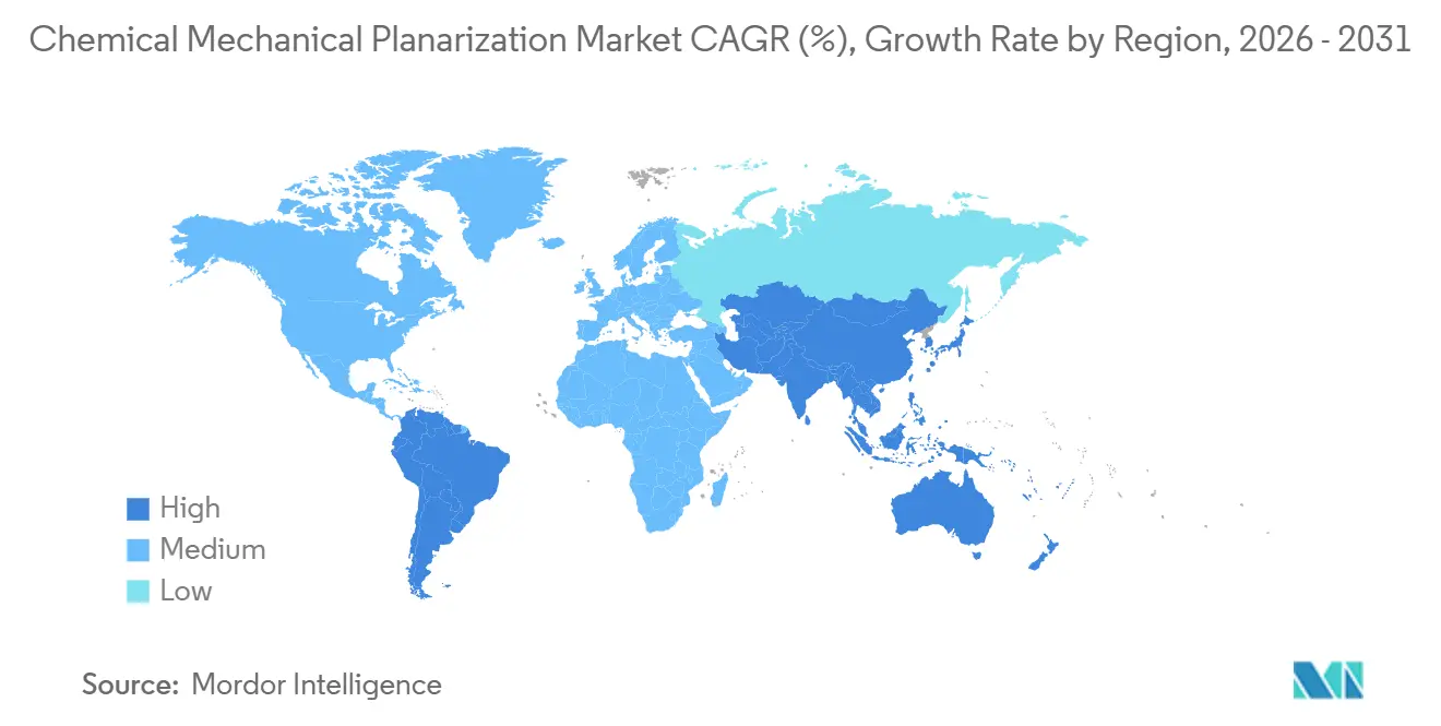
| Fastest Growing Market | Asia Pacific |
| Largest Market | Asia Pacific |
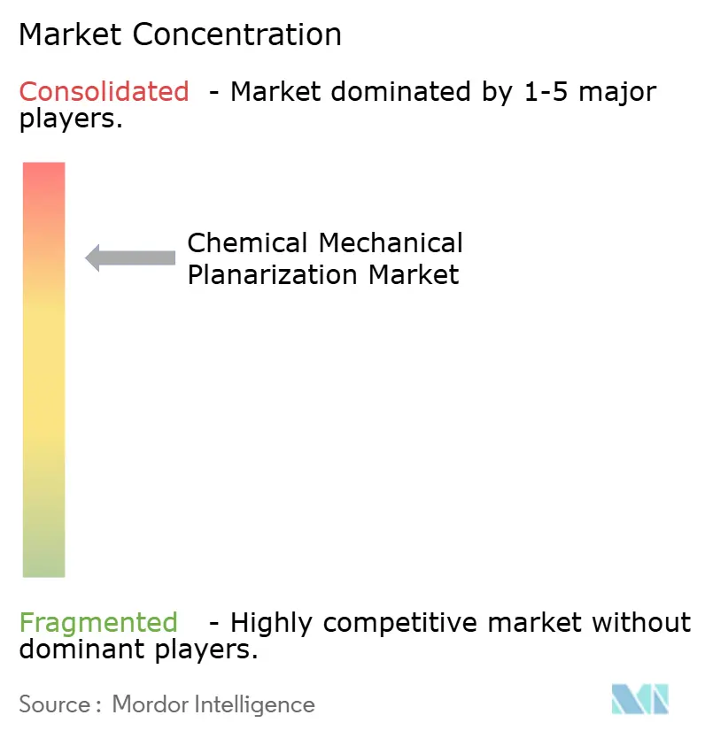
| Market Concentration | High |
Major Players *Disclaimer: Major Players sorted in no particular order Image © Mordor Intelligence. Reuse requires attribution under CC BY 4.0. | |
Chemical Mechanical Planarization Market Analysis by Mordor Intelligence
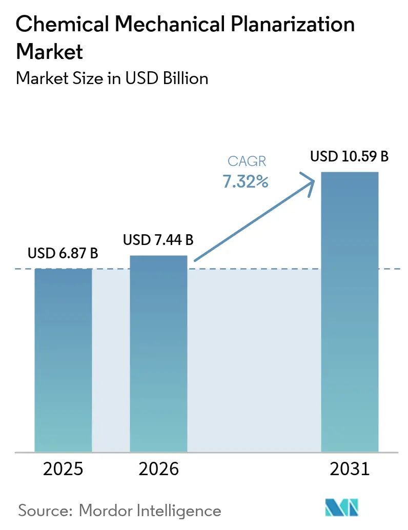
The chemical mechanical planarization market size is projected to be USD 6.87 billion in 2025, USD 7.44 billion in 2026, and reach USD 10.59 billion by 2031, growing at a CAGR of 7.32% from 2026 to 2031. Steady demand for gate-all-around transistors, 3D-IC packaging, and datacenter accelerators is lifting slurry and pad volumes, while localization programs in the United States and Europe shorten delivery cycles and reduce buffer inventory. Asia-Pacific keeps its cost-lead advantage in mature logic and memory nodes, yet North America is adding 300 millimeter capacity faster as CHIPS Act grants require domestic consumables sourcing. Sustainability objectives are nudging fabs toward low-abrasive chemistries that trim defectivity without sacrificing throughput, and electro-chemical-mechanical polishing is gaining pilot acceptance for copper and barrier layers. Equipment retrofits that embed optical profilometry and machine-learning controls are also stretching pad life, compressing consumable waste, and protecting margins despite rare-earth volatility.
Key Report Takeaways
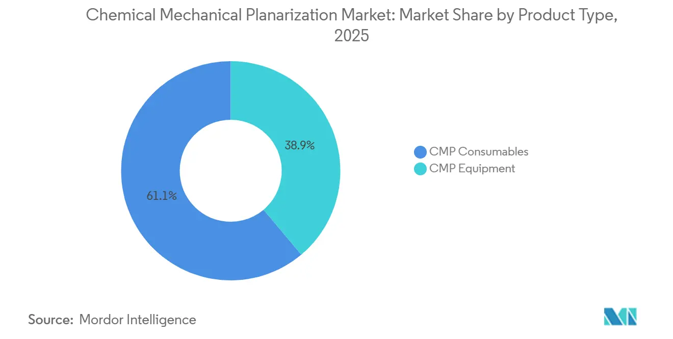
- By product type, CMP consumables led with 61.14% revenue share in 2025, while CMP equipment is forecast to expand at an 8.12% CAGR through 2031.
- By application, integrated circuits accounted for 46.32% of 2025 sales, whereas compound semiconductors are advancing at a 9.84% CAGR to 2031.
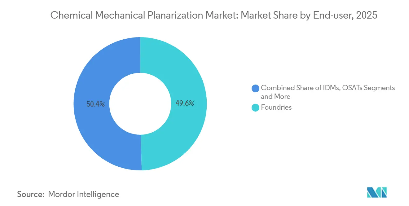
- By end-user, foundries held 49.64% spending in 2025 and outsourced semiconductor assembly and test providers are projected to grow at a 9.45% CAGR over 2026-2031.
- By wafer size, 300 millimeter substrates retained 63.96% of chemical mechanical planarization market share in 2025, while the beyond-450 millimeter segment is set to rise at a 7.86% CAGR.
- By geography, Asia-Pacific captured 54.96% revenue in 2025, although South America is estimated to be the fastest region at an 8.37% CAGR during the forecast period.
Note: Market size and forecast figures in this report are generated using Mordor Intelligence’s proprietary estimation framework, updated with the latest available data and insights as of 2026.
Global Chemical Mechanical Planarization Market Trends and Insights
Drivers Impact Analysis*
| Driver | (~) % Impact on CAGR Forecast | Geographic Relevance | Impact Timeline |
|---|---|---|---|
| Accelerating GAA and 3D-IC Adoption | +1.8% | Global, with early deployment in Taiwan, South Korea, and leading-edge fabs in Arizona | Medium term (2-4 years) |
| Rapid Growth in SiC/GaN Power Devices | +1.5% | APAC core (Japan, China), spill-over to Europe and North America for automotive and renewable energy | Medium term (2-4 years) |
| U.S. and EU Fab Incentives Localizing CMP Supply | +1.3% | North America and Europe, with secondary effects in supply-chain hubs across Southeast Asia | Short term (≤ 2 years) |
| AI Datacenter Capex Pull-Through (Advanced Interconnect Layers) | +1.2% | Global, concentrated in regions with hyperscale datacenter construction (North America, APAC) | Short term (≤ 2 years) |
| Shrinking Node-Specific CMP Step Count | +0.9% | Global, primarily impacting leading-edge fabs in Taiwan, South Korea, and Arizona | Long term (≥ 4 years) |
| Sustainability Push for Low-Abrasive Slurries | +0.6% | Europe and North America, with emerging adoption in Japan and South Korea | Long term (≥ 4 years) |
| Source: Mordor Intelligence | |||


Accelerating GAA and 3D-IC Adoption
Gate-all-around transistors introduce roughly 30% more polishing steps than FinFET nodes because each nanosheet stack must meet nanometer-level topography targets to avoid shorts. Three-dimensional integrated circuits double CMP demand again, as hybrid bonding needs sub-angstrom surfaces on both die before copper-to-copper contact. Pilot lines in Taiwan and South Korea already run 18-22 CMP passes per wafer for 2 nanometer logic, and electro-chemical-mechanical polishing cuts dishing by up to 40%, improving yield on narrow gates.[1]Investor Relations, “Fiscal 2025 Earnings and Product Announcements,” Applied Materials, appliedmaterials.com Equipment shipments of next-generation platforms rose more than 40% in 2025, confirming that mega-fab ramps translate directly into higher consumable.[2]Nature Electronics Editorial Board, “Electro-Chemical-Mechanical Polishing Advances,” nature.com
Rapid Growth in SiC and GaN Power Devices
Silicon carbide hardness demands diamond or alumina abrasives that triple polyurethane pad wear, raising pad change frequency and consumable bills. Wolfspeed’s 2025 production consumed 22% more slurry per wafer than its silicon lines, and dedicated compound-semiconductor bays were installed after 5% yield loss traced to cross-contamination. Entegris answered with a GaN-specific pad that channels slurry to the wafer edge, lowering defectivity 18% in beta trials. Regional automakers and renewable-energy suppliers in Japan, Germany, and the United States now qualify SiC and GaN power modules, expanding CMP demand beyond consumer electronics.
U.S. and EU Fab Incentives Localizing CMP Supply
CHIPS Act recipients must source at least 55% of consumables domestically by 2027, so slurry and pad makers are expanding plants in Illinois, Arizona, and Ohio. BASF is mirroring this move in Germany with a EUR 120 million (USD 132 million) blending site built next to Intel’s Magdeburg fab. These projects cut freight times from months to weeks, trimming buffer inventory and waste. A dual-network model is emerging, with low-cost mass production in Asia-Pacific and agile satellite mixing in the West, balancing cost discipline with geopolitical resilience.[3]Reuters Staff, “Rare Earth Supply Constraints Lift Cerium Prices,” reuters.com
AI Datacenter Capex Pull-Through
Hyperscale operators spent almost USD 200 billion on new datacenters in 2025, and 18% went to substrates that need post-bond CMP to keep co-planarity under 1 micrometer. NVIDIA’s Blackwell interposers use 14 CMP steps per package, twice the prior generation, while SK Hynix will add 36 CMP tools by 2027 for high-bandwidth memory expansion. Closed-loop systems with optical profilometry guarantee 200-nanometer pillar height uniformity, an essential requirement for large accelerator packages. Outsourced semiconductor assembly and test providers therefore placed over USD 300 million in tool orders during 2025, showing that datacenter appetite pulls CMP demand deep into back-end supply chains.
Restraints Impact Analysis*
| Restraint | (~) % Impact on CAGR Forecast | Geographic Relevance | Impact Timeline |
|---|---|---|---|
| Escalating Slurry Input Costs (Rare Earths) | -0.9% | Global, with acute pressure in regions dependent on Chinese cerium oxide exports | Short term (≤ 2 years) |
| Tight OEM Capacity for 300 mm Tools | -0.7% | North America and Europe, where CHIPS Act-funded fabs face equipment delivery delays | Medium term (2-4 years) |
| Cross-Contamination Risk in Hetero-Material CMP | -0.5% | APAC and North America, particularly fabs transitioning to compound semiconductor production | Medium term (2-4 years) |
| China-U.S. Export Controls on High-End Pads and Conditioners | -0.4% | China and allied nations subject to U.S. export restrictions, fragmenting global supply chains | Long term (≥ 4 years) |
| Source: Mordor Intelligence | |||
Escalating Slurry Input Costs (Rare Earths)
China’s 2025 export quotas lifted cerium oxide prices 34% year-over-year, slicing gross margins at major slurry suppliers even after 7% list-price increases. Outside-China refining delivers barely 15% of global supply, and substitution with colloidal silica cuts oxide removal rates by up to 30%, stretching tool cycle time. DuPont’s USD 45 million program for cerium-free chemistries targets a 2027 launch, yet fabs remain exposed in the near term. Smaller regional vendors lacking hedging muscle risk consolidation, with analysts expecting three to five exits before 2028.
Tight OEM Capacity for 300 mm Tools
Lead times for new 300 millimeter platforms stretched to 18 months in early 2026 because motion-control actuators and vacuum chucks remain supply-constrained. EBARA allocated 60% of 2026 output to long-standing customers in Asia, delaying U.S. CHIPS fabs and pushing Intel’s Ohio schedule back six months. Used 300 millimeter gear now commands 40-50% premiums, and fabs extend maintenance cycles while adding predictive analytics to squeeze more wafers from aging fleets. The squeeze raises capital intensity for greenfield projects and threatens delivery milestones tied to subsidy tranches.
*Our forecasts treat driver/restraint impacts as directional, not additive. The impact forecasts reflect baseline growth, mix effects, and variable interactions.
Segment Analysis
By Product Type: Equipment Retrofits Narrow the Gap
CMP consumables delivered 61.14% of 2025 revenue, reflecting their recurring nature and direct linkage to wafer volume, while equipment is forecast to climb at an 8.12% CAGR as fabs retrofit legacy lines with machine-learning endpoint controls. Slurries capture roughly 55% of consumable spend, and barrier chemistries rise fastest because gate-all-around nodes require selective removal of tantalum nitride without copper loss, bolstering chemical mechanical planarization market demand. Pads contribute 30% of outlay, with micro-textured designs extending pad life 25% and shrinking downtime. Diamond conditioners face export restrictions that shift supply toward France and the United States, reshaping regional purchasing.
Equipment orders accelerate as closed-loop profilometry lets operators tune pad pressure and slurry flow on the fly, elevating overall equipment effectiveness. Applied Materials’ machine-trained algorithms predict pad-conditioning cycles with 95% accuracy, cutting unplanned stops by 30%. EBARA’s modular heads switch between silicon and silicon carbide recipes in 15 minutes, addressing cross-contamination fears. Revasum’s tools optimized for 200 millimeter SiC substrates recorded a 62% booking jump in 2025, proving that agile niche players can ride compound-semiconductor momentum in the chemical mechanical planarization market.

By Application: Compound Semiconductors Punch Above Weight
Integrated circuits still accounted for 46.32% of 2025 revenue, but compound semiconductors are forecast to grow 9.84% per year as electric vehicles and renewable grids adopt silicon carbide and gallium nitride power modules. Logic devices at 3 nanometers demand up to 22 CMP passes, especially for backside power networks that need wafer thinning plus re-polishing. High-bandwidth memory stacks lift consumable volumes because each die in a 12-layer sandwich requires through-silicon via reveal steps.
Silicon carbide modules require removal rates below 0.5 micrometers per minute to protect crystal integrity, stretching polish time to eight minutes per wafer and inflating slurry bills. Gallium nitride radio-frequency wafers need 0.2 nanometer surface finish to minimize millimeter-wave losses. Advanced packaging, including fan-out wafer-level and 2.5D interposers, grew 11% in 2025 and keeps adding CMP steps post-redistribution layer, anchoring diverse end-markets inside the chemical mechanical planarization market size envelope.
By End-User: OSAT Spending Accelerate
Foundries absorbed 49.64% of 2025 purchases because they pilot leading-edge nodes first and own the densest CMP tool fleets. Taiwan Semiconductor Manufacturing Company and Samsung Foundry together bought over one-third of global slurry and pad tons last year, anchoring economies of scale. Integrated device manufacturers captured 28% but leverage in-house design to secure 15-20% consumable discounts, pressuring independent peers.
Outsourced semiconductor assembly and test providers grow fastest at 9.45% CAGR by installing CMP in back-end lines for hybrid bonding. ASE committed USD 1.2 billion to expand fan-out wafer-level packaging capacity, adding 18 CMP tools in Taiwan and Malaysia. Amkor boosted CMP capex 48% in 2025 to support accelerator packages in Arizona and Vietnam. Research institutes remain below 3% of spending yet influence chemistry trials that underpin future launches, highlighting their intangible weight in the chemical mechanical planarization industry.

By Wafer Size: Beyond-450 mm Still Experimental
The 300 millimeter format retained 63.96% of chemical mechanical planarization market share in 2025 as more than 250 fabs polish on this diameter, and utilization averaged 82% worldwide. OEM lead-time constraints force fabs to sweat assets longer, and predictive analytics extract extra wafers between pad changes.
Pilot 450 millimeter programs gained momentum after SEMI issued updated handling rules that widen wafer-edge exclusion zones to 5 millimeters, trimming net die yield gains. Intel signaled interest in post-2030 adoption if CMP can reach 2% within-wafer non-uniformity on the larger diameter. Applied Materials and EBARA each demoed prototypes, yet the chemical mechanical planarization market size uplift hinges on synchronized lithography and etch readiness, extending commercial timelines into the next decade.
Geography Analysis
Asia-Pacific generated 54.96% of 2025 revenue and remains the epicenter of high-volume production. Taiwan Semiconductor Manufacturing Company alone operated more than 120 CMP tools across three campuses to support 2 nanometer logic, drawing substantial slurry imports through established logistics lanes. South Korea followed with memory-focused demand, where through-silicon via reveal doubles consumable use per die stack. China advanced CMP consumption 6% despite export controls because domestic fabs added 28-nanometer capacity for automotive chips, leveraging mature equipment exempt from recent restrictions.
North America is projected to rise at a 7.8% CAGR, reflecting CHIPS Act incentives that tether slurry and pad plants to new fabs in Arizona, Ohio, and Texas. Entegris and Cabot Microelectronics each broke ground on facilities within 80 kilometers of Intel’s Ohio campus, slicing delivery cycles from eight weeks to below two and strengthening just-in-time models. Taiwan Semiconductor Manufacturing Company’s Arizona site began installing 24 new CMP tools in late 2026, marking the largest single-wave tool delivery into the United States in more than a decade. Samsung’s Taylor project confronted a four-month delay in CMP arrival, demonstrating how OEM capacity shortages remain a gating item for Western expansions.
Europe will expand at a 7.5% pace through 2031 as the EU Chips Act funnels EUR 43 billion into fabs, materials, and workforce programs. Intel’s Magdeburg plant secured EUR 10 billion (USD 11 billion) in subsidies and plans to install 30 CMP tools by 2029 for its 18A node, which doubles polishing steps thanks to backside power delivery. The European Semiconductor Manufacturing Company joint venture has 28-nanometer and 22-nanometer lines scheduled for 2027 start-up in Dresden, anchoring automotive-grade demand that values reliability over absolute density. South America remains small but fastest, climbing 8.37% as Brazil and Argentina use tax credits to entice outsourced semiconductor assembly and test investors who install post-bond CMP bays in proximity to automotive electronics clusters.

Competitive Landscape
The chemical mechanical planarization market shows moderate concentration, with the top three tool makers holding roughly 70% revenue while consumables stay more fragmented. Applied Materials leverages its installed base of more than 3,000 platforms to bundle predictive maintenance subscriptions that generated USD 420 million in service revenue during 2025, deepening customer lock-in. Entegris’ 2022 purchase of CMC Materials yielded about 40% global slurry and pad share, letting it cross-sell post-CMP cleans in a single invoice and standardize quality across multisite customers.
Smaller specialists chase high-growth niches. Revasum tailors 200 millimeter SiC tools that carry 15-20% price premiums because mainstream platforms cannot manage the material’s hardness without slowdowns. Okamoto and Tokyo Seimitsu court MEMS and optical sensors that need gentle touch and micron-scale runout. Disruptive entrants promote electro-chemical-mechanical polishing that halves abrasive loads, gaining traction among cost-sensitive Chinese and Indian fabs, while Ace Nanochem’s per-wafer pricing shifts inventory risk off fab ledgers, appealing to research institutes with erratic volumes.
Patent momentum underscores innovation intensity. Filings for electro-chemical-mechanical designs climbed 22% in 2025, with Lam Research integrating anodic cells into platens for real-time dissolution control. Standards bodies respond quickly; SEMI’s CMP Users Group captures best practices on pad conditioning and slurry recirculation, with 80% of global operators attending its workshops. Capital spending therefore clusters around suppliers that combine hardware, chemistry, and software into cohesive ecosystems, a pattern likely to harden entry barriers over the forecast horizon.
Chemical Mechanical Planarization Industry Leaders
Applied Materials Inc.
Entegris Inc.
Lapmaster Wolters Gmbh
EBARA Corporation
DuPont de Nemours, Inc.
- *Disclaimer: Major Players sorted in no particular order

Recent Industry Developments
- February 2026: Applied Materials shipped its 100th Reflexion LK platform to Taiwan Semiconductor Manufacturing Company’s Hsinchu site, supporting 2 nanometer mass production.
- January 2026: Entegris completed a USD 200 million slurry-plant expansion in Kulim, Malaysia, boosting regional capacity 35%.
- December 2025: BASF secured EUR 120 million (USD 132 million) under the EU Chips Act for a Magdeburg slurry facility scheduled for 2027 start-up.
- November 2025: DuPont launched a USD 45 million program to commercialize cerium-free shallow-trench isolation slurries by 2027.


Global Chemical Mechanical Planarization Market Report Scope
Chemical Mechanical Planarization (CMP) is a precision polishing process used in semiconductor manufacturing to make a wafer surface perfectly flat and smooth. It combines chemical reactions and mechanical abrasion to remove tiny amounts of material from the surface.
The Chemical Mechanical Planarization Report is Segmented by Product Type (CMP Equipment, CMP Consumables), Application (Integrated Circuit, Compound Semiconductor, MEMS and NEMS, Advanced Packaging, Other Applications), End-User (Foundries, IDMs, OSAT, R&D Institutes), Wafer Size (200 mm, 300 mm, 450 mm, Beyond 450 mm), and Geography (North America, South America, Europe, Asia-Pacific, Middle East, Africa). Market Forecasts are Provided in Terms of Value (USD).
| CMP Equipment |
| CMP Consumables |
| Integrated Circuit |
| Compound Semiconductor |
| MEMS and NEMS |
| Advanced Packaging |
| Other Applications |
| Foundries |
| Integrated Device Manufacturers (IDMs) |
| Outsourced Semiconductor Assembly and Test (OSAT) |
| R&D Institutes / Universities |
| 200 mm |
| 300 mm |
| 450 mm |
| Beyond 450 mm |
| North America | United States |
| Canada | |
| Mexico | |
| South America | Brazil |
| Argentina | |
| Rest of South America | |
| Europe | Germany |
| United Kingdom | |
| France | |
| Italy | |
| Spain | |
| Rest of Europe | |
| Asia-Pacific | China |
| India | |
| Japan | |
| South Korea | |
| Australia and New Zealand | |
| Rest of Asia-Pacific | |
| Middle East | Saudi Arabia |
| United Arab Emirates | |
| Turkey | |
| Rest of Middle East | |
| Africa | South Africa |
| Nigeria | |
| Egypt | |
| Rest of Africa |
| By Product Type | CMP Equipment | |
| CMP Consumables | ||
| By Application | Integrated Circuit | |
| Compound Semiconductor | ||
| MEMS and NEMS | ||
| Advanced Packaging | ||
| Other Applications | ||
| By End-User | Foundries | |
| Integrated Device Manufacturers (IDMs) | ||
| Outsourced Semiconductor Assembly and Test (OSAT) | ||
| R&D Institutes / Universities | ||
| By Wafer Size | 200 mm | |
| 300 mm | ||
| 450 mm | ||
| Beyond 450 mm | ||
| By Geography | North America | United States |
| Canada | ||
| Mexico | ||
| South America | Brazil | |
| Argentina | ||
| Rest of South America | ||
| Europe | Germany | |
| United Kingdom | ||
| France | ||
| Italy | ||
| Spain | ||
| Rest of Europe | ||
| Asia-Pacific | China | |
| India | ||
| Japan | ||
| South Korea | ||
| Australia and New Zealand | ||
| Rest of Asia-Pacific | ||
| Middle East | Saudi Arabia | |
| United Arab Emirates | ||
| Turkey | ||
| Rest of Middle East | ||
| Africa | South Africa | |
| Nigeria | ||
| Egypt | ||
| Rest of Africa | ||


Key Questions Answered in the Report
What CAGR is projected for chemical mechanical planarization demand between 2026 and 2031?
The market is forecast to grow at a 7.32% CAGR from 2026 to 2031, reaching USD 10.59 billion by the end of the period.
Which region currently generates the most CMP revenue?
Asia-Pacific leads with 54.96% of 2025 revenue thanks to high-volume production in Taiwan, South Korea, and China.
Why are consumables still the largest spending category?
Slurries, pads, and conditioners scale directly with wafer starts, giving them 61.14% of 2025 revenue even as equipment retrofits accelerate.
How do CHIPS Act incentives influence CMP supply chains?
U.S. subsidies require rising domestic content, so slurry and pad makers are building plants near new fabs in Arizona, Ohio, and Texas to cut lead times.
What is driving the fastest application growth?
Compound semiconductors, especially silicon carbide and gallium nitride devices for electric vehicles and renewable grids, are growing at 9.84% CAGR through 2031.
Are 450 millimeter CMP tools commercially available?
Prototype platforms exist, but broad deployment is unlikely before 2030 because supporting lithography and etch tools are not yet synchronized.
Page last updated on:


