
Ajinomoto Build-up Film Market Size and Share
Market Overview
| Study Period | 2021 - 2031 |
|---|---|
| Market Size (2026) | USD 10.73 Billion |
| Market Size (2031) | USD 22.97 Billion |
| Growth Rate (2026 - 2031) | 16.45 % |
| Fastest Growing Market | North America |
| Largest Market | Asia-Pacific |
| Market Concentration | High |
Major Players *Disclaimer: Major Players sorted in no particular order Image © Mordor Intelligence. Reuse requires attribution under CC BY 4.0. | |
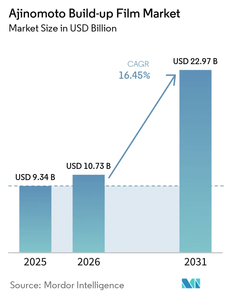
Ajinomoto Build-up Film Market Analysis by Mordor Intelligence
The Ajinomoto Build-up Film market size was valued at USD 9.34 billion in 2025 and is estimated to grow from USD 10.73 billion in 2026 to USD 22.97 billion by 2031, at a CAGR of 16.45% during the forecast period (2026-2031). AI accelerator packages require 8 to 16 buildup film layers, compared with 4 to 6 layers in legacy PC processors, thereby increasing film consumption per advanced package. Ajinomoto identifies Ajinomoto Build-up Film (ABF) as a standard material used across generations of high-performance semiconductor packages, and its high-performance computing (HPC)-related ABF shipment outlook points to demand growth. This pattern makes the ABF market more dependent on both package complexity and semiconductor shipment figures. Capacity plans by major substrate producers indicate that organic substrates will remain important for AI server production through 2028. Long qualification cycles and concentrated film supply can limit the ABF market's ability to respond quickly to rising demand. The ABF market also depends on alignment among film output, substrate yields, and chip designers' product schedules. A delay in any one of these steps can limit deliveries even when end demand remains strong. The ABF market consequently favors suppliers that can coordinate capacity with qualified customers. This coordination is important because package material, substrate process, and final device requirements are closely linked.
Key Report Takeaways
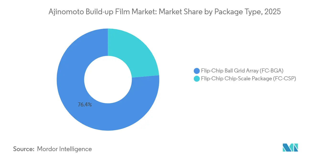
- By package type, Flip-Chip Ball Grid Array (FC-BGA) held 76.37% of the Ajinomoto Build-up Film market share in 2025, while FC-BGA is also forecast to expand at an 18.45% CAGR through 2031.
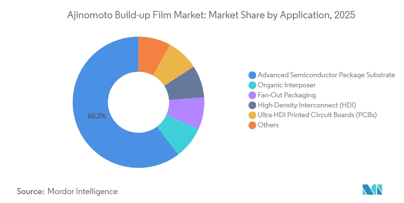
- By application, Advanced Semiconductor Package Substrate held 60.34% of the Ajinomoto Build-up Film market share in 2025, while Organic Interposer is forecast to expand at a 20.37% CAGR through 2031.
- By geography, Asia-Pacific held 51.82% of Ajinomoto Build-up Film market share in 2025, while North America is forecast to expand at an 19.21% CAGR through 2031.
Note: Market size and forecast figures in this report are generated using Mordor Intelligence’s proprietary estimation framework, updated with the latest available data and insights as of January 2026.
Global Ajinomoto Build-up Film Market Trends and Insights
Drivers Impact Analysis*
| Drivers | (~) % Impact on CAGR Forecast | Geographic Relevance | Impact Timeline |
|---|---|---|---|
| AI Accelerator and Hyperscale Data-Center Buildout | +5.50% | Global | Short term (≤ 2 years) |
| Rising Package Layer Counts and Chiplet Architectures | +3.50% | Asia-Pacific, North America | Medium term (2-4 years) |
| Expansion of High-Speed Networking and Custom Application-Specific Integrated Circuits (ASICs) | +2.50% | North America, Asia-Pacific | Medium term (2-4 years) |
| Mainstreaming of Advanced Packaging in Automotive Electronics | +2.00% | Europe, Asia-Pacific, North America | Long term (≥ 4 years) |
| Organic Interposer Adoption for Lower-Loss, Lower-Cost Integration | +1.50% | Asia-Pacific core, spillover to North America | Medium term (2-4 years) |
| Source: Mordor Intelligence | |||
AI Accelerator and Hyperscale Data-Center Buildout
AI accelerator deployment in hyperscale data centers is the primary driver of demand for the Ajinomoto Build-Up Film (ABF) market. New accelerator generations combine more chiplets, higher memory bandwidth, and larger die areas, which require more build-up layers and larger substrate footprints. Ajinomoto Fine-Techno lines are operating at full utilization in 2026, while the company's new Chubu facility is not scheduled to begin production until 2032.
New film capacity can take 5 to 6 years from investment approval to first output, making film capacity a more immediate constraint than substrate capacity in the ABF market. Near-term demand increases are therefore likely to be managed through customer allocation rather than rapid output additions. Allocation tends to favor substrate producers with established relationships and qualified products, creating a tighter connection between supply availability and long-standing commercial partnerships. This condition also raises the importance of production planning for customers serving AI infrastructure programs, as customer forecasts and qualified capacity matter before new accelerator programs move into production. The effect is strongest where a substrate design depends on material already approved for a particular package stack.
Rising Package Layer Counts and Chiplet Architectures
Chiplet-based heterogeneous integration has shifted substrate requirements toward earlier design collaboration, with substrate suppliers now working with foundries and chip designers before tape-out. SEMI materials data indicate that chiplet architectures can require microvias below 50 micrometers and redistribution layers at 2 micrometers pitch, pushing ABF films toward tighter physical and electrical specifications. Standard film grades remain suited to legacy PC substrates and mid-range networking devices, while advanced low-coefficient of thermal expansion (CTE) and low-loss grades address the needs of more demanding package designs.
The separation between standard and advanced grades creates a more segmented ABF market. Advanced variants carry different material requirements and longer qualification periods. Substrate manufacturers must hold line-width and via-pitch tolerances through the complete build-up stack, placing qualified producers inside advanced packaging programs before product tape-out. Ajinomoto presented technical work in 2025 on warpage control, stress absorption, and multi-material stack compatibility, demonstrating how film specifications are developed with foundry and substrate partners. This development process links film selection to package performance requirements before commercial output is produced, leaving less scope for material changes once a program has reached design lock.
Expansion of High-Speed Networking and Custom Application-Specific Integrated Circuits (ASICs)
High-speed switch application-specific integrated circuits (ASICs) and custom accelerator chips represent an additional source of demand for the ABF market. Cloud operators use custom silicon for internal AI clusters alongside GPU-based systems, with each platform requiring its own substrate development and qualification work. This is not a replacement of GPU demand but rather adds separate product programs to the workload handled by substrate manufacturers, broadening the set of customers that need advanced package substrates.
Broadcom stated that it was establishing substrate production capacity in Singapore beginning in FY2027 to address supply constraints affecting custom AI accelerator programs, indicating that substrate availability has become a material issue for chip developers. Each custom ASIC can create an independent qualification queue at a substrate manufacturer. Suppliers able to manage concurrent programs can retain customers across several product generations, with those relationships becoming more durable as switching costs accumulate with each new design. This supports demand for qualified film materials used in advanced substrate builds. The wider platform mix does not simplify procurement, as each program can use a different package design and set of operating requirements. It instead increases the need for suppliers that can support several qualified builds simultaneously.
Mainstreaming of Advanced Packaging in Automotive Electronics
Automotive electronics are moving from wire-bond BGA substrates toward FC-BGA platforms for ADAS and autonomous driving processors, which require greater pin counts, thermal management, and interconnect density. These requirements increasingly resemble those found in high-end server packages. IMAPS research reports that lidded and bare-die FC-BGA packages can meet AEC Grade 2 reliability conditions with appropriate substrate core and build-up dielectric selections. The cited testing included 150°C high-temperature storage for 500 hours and thermal cycling from -55°C to 125°C for 1,000 cycles.
AEC-Q100 Grade 1 and Grade 0 requirements include a 15-year reliability life and 150°C device operating conditions[1]. These requirements create a separate qualification path for automotive film formulations and substrate designs, with suppliers required to complete different testing, approval, and material validation processes. Automotive-grade ABF demand currently represents a single-digit portion of total output. It is growing faster than the broader market and supports higher pricing after certification. This gives qualified suppliers a reason to develop products for automotive packaging programs. The value of the opportunity depends on completing the reliability process rather than simply supplying standard server-grade material, a distinction that keeps automotive demand separate from mainstream data center requirements.
Restraints Impact Analysis*
| Restraints | (~) % Impact on CAGR Forecast | Geographic Relevance | Impact Timeline |
|---|---|---|---|
| Long Qualification Cycles for New Film Formulations | -1.20% | Global | Short term (≤ 2 years) |
| Yield Loss at High Layer Counts and Ultra-Fine Line Widths | -0.90% | Asia-Pacific, North America | Medium term (2-4 years) |
| Single-Supplier Exposure in Leading-Edge ABF Film | -0.60% | Global | Short term (≤ 2 years) |
| Source: Mordor Intelligence | |||
Long Qualification Cycles for New Film Formulations
Long qualification cycles limit how quickly new ABF formulations can enter production. Film candidates must undergo thermal cycling, damp-heat aging, electrical characterization, and batch consistency validation. Testing is completed with the full substrate stack, package design, and relevant operating environment. Industry practice places the qualification process for advanced formulations at 1-3 years. This reflects the high value at risk after wafer fabrication, advanced package assembly, and High Bandwidth Memory (HBM) integration. A late material failure can affect a finished package worth thousands of dollars.
The qualification process creates a material barrier to entry into the Ajinomoto Build-up Film market. A technically capable film developer can face a multi-year period before significant sales begin. JEDEC (Joint Electron Device Engineering Council) and IPC (Association Connecting Electronics Industries) reliability standards specify test methods and sample requirements that add time to approval programs. Thermocompression bonding for advanced chiplet packages introduces further test requirements. Alternative developers in Taiwan and China are in pilot production and customer testing. Their progress does not immediately resolve supply limits because they face the same approval timetable. A pilot line can demonstrate material potential, but it does not remove the need for customer-specific validation. This gap between technical readiness and commercial approval slows the arrival of alternative film supply.
Yield Loss at High Layer Counts and Ultra-Fine Line Widths
ABF substrates with more than 14 layers require over 60 sequential manufacturing steps. Cumulative panel yields of 75% to 80% mean that some substrate area is lost before shipment. Higher layer counts and larger AI packages increase this loss. Advanced AI chip substrates use 5 to 10 times as much area as legacy PC packages. This reduces the number of packages produced per manufacturing panel and changes the economics of existing substrate lines.
The impact of yield loss compounds as layer count rises. Manufacturers are investing in Semi-Additive Process (SAP) and modified SAP equipment for line and space resolution below 2 micrometers. This equipment does not produce salable output until yield learning stabilizes, a period that typically requires 1 to 2 years of production-line qualification. European and North American greenfield projects face a disadvantage relative to established Asian lines with existing yield experience. IEEE research also identifies Coefficient of Thermal Expansion (CTE)-matched dielectric materials and metallic stiffeners as important for warpage control at advanced layer counts. The need to balance these variables adds complexity during process development and limits the speed of a production ramp. It also makes established process knowledge important when manufacturers pursue finer features.
*Our forecasts treat driver/restraint impacts as directional, not additive. The impact forecasts reflect baseline growth, mix effects, and variable interactions.
Segment Analysis
By Package Type: FC-BGA Supports Advanced AI Package Requirements
Flip-Chip Ball Grid Array (FC-BGA) held 76.37% of the Ajinomoto Build-up Film market share in 2025 and is expected to grow at an 18.45% CAGR through 2031. Its position reflects years of use in high-pin-count and high-thermal-power applications. FC-BGA can handle more than 10,000 signals and thermal design powers above 300 W, meeting the requirements of current GPU and custom ASIC platforms. Chiplet designs are also driving FC-BGA toward multi-cavity layouts, which can accommodate co-packaged optical elements and embedded silicon bridges.
The added package complexity raises both substrate content and selling prices. Ibiden committed JPY 500 billion (equivalent to USD 3.1 billion) across FY2026 to FY2028 for high-performance IC substrate capacity serving AI servers. This investment points to an extended capacity cycle for FC-BGA rather than a mature demand profile. Flip-Chip Chip Scale Package (FC-CSP) serves mobile SoCs, 5G modems, and mid-range computing devices with tighter form-factor requirements. Its growth is more moderate due to a mature smartphone supply chain and slower layer-count growth. JEDEC JESD22 and IPC-6012 requirements for FC-CSP also slow material substitution and favor established suppliers, as these requirements must be met alongside the performance and form-factor needs of mobile devices. This contrasts with FC-BGA, illustrating why material grades are developed for distinct packaging conditions.

By Application: Advanced Package Substrates Lead While Organic Interposers Expand
The Advanced Semiconductor Package Substrate accounted for 60.34% of the Ajinomoto Build-up Film market share in 2025. It is the primary interconnect platform for CPUs, GPUs, and custom AI ASICs. The substrate's design role grows as semiconductor architectures shift from monolithic to chiplet designs, reinforcing the application's revenue position. Organic Interposer represents the fastest-growing application and is projected to grow at a 20.37% CAGR through 2031. Panel-level production supports a lower cost per connection for relevant chiplet programs.
Shinko Electric's i-THOP uses thin-film technology and a 2.3D structure within an organic interposer. The design aims to approach the density of silicon interposers while retaining the benefits of panel-scale processing. Fan-Out Packaging uses ABF films selectively in embedded-die configurations. High-Density Interconnect (HDI) and Ultra-HDI printed circuit boards serve AI server motherboards and networking switch boards. ABF-derived processing methods are moving into HDI fabrication as line-width requirements fall below 10 micrometers. Other applications include embedded bridge packaging and coreless substrates for thin mobile packages. Embedded bridge approaches use ABF layers as an interchip connection medium between bridging dies and organic substrates. Coreless formats are well-suited to applications where low package height is a primary requirement.
Geography Analysis
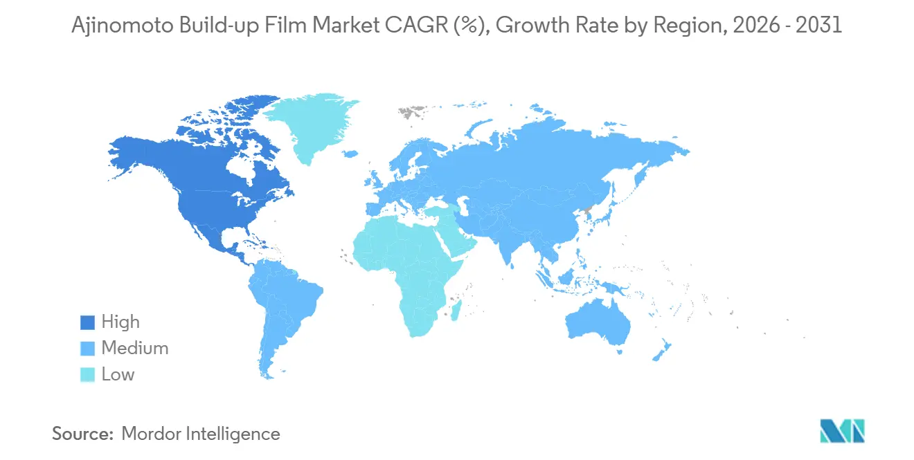
Asia-Pacific held 51.82% of the Ajinomoto Build-up Film market share in 2025 and remains the primary production center. Japan hosts key Ajinomoto Fine-Techno film operations, while Taiwan and South Korea hold major Flip-Chip Ball Grid Array (FC-BGA) capacity through Unimicron, Kinsus, LG Innotek, and Samsung Electro-Mechanics. Japan also contributes through Ibiden. China-based Shennan Circuits and Fastprint are progressing toward advanced ABF substrate production; however, their qualification progress at the highest layer counts remains slower than their capital commitments suggest. This indicates that investment alone does not determine access to the most demanding substrate programs, as process maturity and customer approval remain decisive for advanced production.
Malaysia is emerging as a secondary manufacturing location through AT&S's Kulim expansion. The company disclosed a EUR 1.5 billion to EUR 2.0 billion program supported by long-term customer commitments from AMD and a second technology company. Samsung Electro-Mechanics and LG Innotek capacities were reportedly near 90% utilization in the first half of 2026, indicating that existing regional capacity was absorbed by AI demand before new lines reached production readiness. North America is the fastest-growing region, with the Ajinomoto Build-up Film market size projected to increase at a 19.21% CAGR through 2031. The region benefits from concentrated policy support and supply-chain diversification requirements. The Ajinomoto Build-up Film market is interested in these programs because local packaging capacity can increase demand for qualified substrate materials. The pace of that demand will depend on successful equipment installation, process learning, and customer qualification. Customer mandates for a non-Asia-Pacific supply source can increase qualification activity even where local production costs are higher, and commercial deliveries will follow the longer greenfield qualification cycle rather than the initial investment announcement.
The U.S. Department of Commerce finalized USD 1.4 billion in National Advanced Packaging Manufacturing Program (NAPMP) awards in January 2025, with USD 300 million allocated to advanced substrate and materials research involving Absolics, Applied Materials, and Arizona State University. Intel's USD 7.86 billion CHIPS Act award includes advanced packaging facilities in Arizona, New Mexico, Ohio, and Oregon[2]. Europe centers on AT&S development activity in Austria and manufacturing activity in Malaysia, while Germany supports automotive-related demand. South America, the Middle East, and Africa remain early-stage consumption markets, with Brazil and Saudi Arabia investing in broader electronics infrastructure.
Competitive Landscape
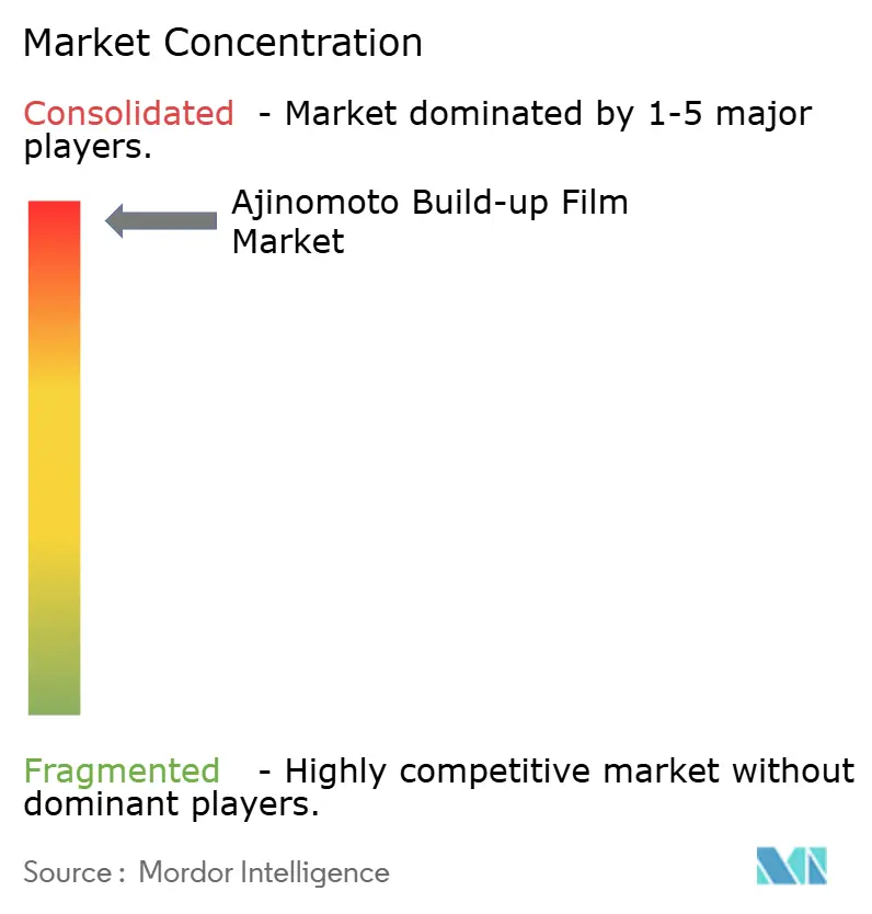
The Ajinomoto Build-up Film market is consolidated. Ajinomoto Fine-Techno holds the dominant position, while Sekisui Chemical is the principal secondary commercial supplier. WaferChem's Taiwan Build-up Film program remains at a small-scale customer verification. Ibiden, Unimicron, AT&S, Shinko Electric, and Kinsus lead substrate conversion. LG Innotek and Shennan Circuits hold complementary positions. Leading suppliers combine material qualification expertise with production scale. Their position is reinforced by the 18- to 24-month qualification cycle associated with material changes. New suppliers must demonstrate both technical performance and consistent output before they can be considered for displacement.
Competitive activity increasingly resembles design support rather than commodity supply. Substrate engineers work with foundry packaging centers during product development, making displacement more difficult once a design is qualified. An established supplier can therefore benefit from earlier involvement in the development of materials and packaging. Late entrants must demonstrate comparable reliability and manufacturing consistency before competing for the same design program. This requirement strengthens the commercial value of existing qualifications. AT&S reported that long-term customer agreements support its EUR 1.0-1.2 billion FY2026/27 capital plan.
Automotive-grade ABF substrates, panel-scale organic interposers, and North American substrate capacity remain areas where new investment is relevant. Automotive programs have high reliability requirements and long approval periods. Organic interposer production has a developing cost-performance case, but output leadership has not been established. Glass-core substrates appear in long-range roadmaps but are not expected to reach commercial scale before 2030. ABF-based organic substrates retain cost and yield-learning advantages through the late 2020s. Bilateral supply agreements are likely to shape access to advanced substrate capacity for the remainder of the decade. These agreements reduce the role of open-market purchases for the most advanced capacity and more closely align expansion decisions with the requirements of committed chip and hyperscale customers.
Ajinomoto Build-up Film Industry Leaders
-
Ajinomoto Co., Inc.
-
SEKISUI CHEMICAL CO.,LTD.
-
WaferChem
-
Resonac Holdings Corporation
-
Kyocera Corporation
- *Disclaimer: Major Players sorted in no particular order
Recent Industry Developments
- June 2026: Ibiden and Unimicron announced a combined capital deployment exceeding USD 5 billion for Ajinomoto Build-up Film (ABF) substrate production for AI servers. Ibiden targets approximately 2.5 times its FY2024 capacity by FY2028, with the Ono Plant and Gama Cell 6 facilities as the primary production sites.
- August 2025: Intel and the Trump Administration reached an agreement on semiconductor manufacturing investment. Intel's combined CHIPS Act-related package totaled USD 11.1 billion, including USD 7.86 billion in direct grants for manufacturing and advanced packaging facilities in Arizona, New Mexico, Ohio, and Oregon.
Global Ajinomoto Build-up Film Market Report Scope
Ajinomoto Build-up Film (ABF) is a specialized insulating film used in the packaging of microchips and computer processors. It serves as a dielectric layer in advanced semiconductor packaging, enabling the formation of fine circuit patterns on substrates. ABF is applied in multiple layers during the build-up process, allowing for high-density interconnections between the chip and the printed circuit board.
The ajinomoto build-up film market is segmented by package type, application, and geography. By package type, the market is segmented into flip-chip ball grid array (FC-BGA) and flip-chip chip-scale package (FC-CSP). By application, the market is segmented into advanced semiconductor package substrate, organic interposer, fan-out packaging, high-density interconnect (HDI), ultra-HDI printed circuit boards (PCBs), and others. The report also covers market size and forecasts for ajinomoto build-up film across 15 countries in major regions. The market sizes and forecasts are provided in terms of value (USD).
| Flip-Chip Ball Grid Array (FC-BGA) |
| Flip-Chip Chip-Scale Package (FC-CSP) |
| Advanced Semiconductor Package Substrate |
| Organic Interposer |
| Fan-Out Packaging |
| High-Density Interconnect (HDI) |
| Ultra-HDI Printed Circuit Boards (PCBs) |
| Others |
| Asia-Pacific | China |
| India | |
| Japan | |
| South Korea | |
| ASEAN Countries | |
| Rest of Asia-Pacific | |
| North America | United States |
| Canada | |
| Mexico | |
| Europe | Germany |
| United Kingdom | |
| France | |
| Italy | |
| NORDIC Countries | |
| Rest of Europe | |
| South America | Brazil |
| Argentina | |
| Rest of South America | |
| Middle East and Africa | Saudi Arabia |
| South Africa | |
| Rest of Middle East and Africa |
| By Package Type | Flip-Chip Ball Grid Array (FC-BGA) | |
| Flip-Chip Chip-Scale Package (FC-CSP) | ||
| By Application | Advanced Semiconductor Package Substrate | |
| Organic Interposer | ||
| Fan-Out Packaging | ||
| High-Density Interconnect (HDI) | ||
| Ultra-HDI Printed Circuit Boards (PCBs) | ||
| Others | ||
| By Geography | Asia-Pacific | China |
| India | ||
| Japan | ||
| South Korea | ||
| ASEAN Countries | ||
| Rest of Asia-Pacific | ||
| North America | United States | |
| Canada | ||
| Mexico | ||
| Europe | Germany | |
| United Kingdom | ||
| France | ||
| Italy | ||
| NORDIC Countries | ||
| Rest of Europe | ||
| South America | Brazil | |
| Argentina | ||
| Rest of South America | ||
| Middle East and Africa | Saudi Arabia | |
| South Africa | ||
| Rest of Middle East and Africa | ||
Key Questions Answered in the Report
What is current market size of Ajinomoto Build-up Film Market?
The Ajinomoto Build-up Film market size was valued at USD 9.34 billion in 2025 and is estimated to grow from USD 10.73 billion in 2026 to USD 22.97 billion by 2031, at a CAGR of 16.45% during the forecast period (2026-2031).
Which package type leads Ajinomoto Build-up Film (ABF) use?
FC-BGA held a 76.37% share in 2025 and is projected to grow at an 18.45% CAGR through 2031. The format supports more than 10,000 signals and thermal design powers above 300 W for demanding Graphics Processing Unit (GPU) and Application-Specific Integrated Circuit (ASIC) packages.
Which application is growing fastest?
Organic Interposer is projected to grow at a 20.37% CAGR through 2031. Panel-level production can lower connection costs by avoiding backside grinding steps required for silicon interposers, while offering suitable interconnect density for mid-tier chiplet programs.
Which region is expanding fastest?
North America is projected to grow at a 19.21% CAGR through 2031. U.S. advanced packaging awards and domestic capacity plans support a more geographically diversified substrate supply base, though qualification lead times remain substantial.