
X-Ray Laminography Inspection Systems Market Size and Share
Market Overview
| Study Period | 2020 - 2031 |
|---|---|
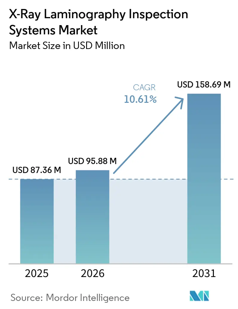
| Market Size (2026) | USD 95.88 Million |
| Market Size (2031) | USD 158.69 Million |
| Growth Rate (2026 - 2031) | 10.61 % |
| Fastest Growing Market | Asia-Pacific |
| Largest Market | Asia-Pacific |
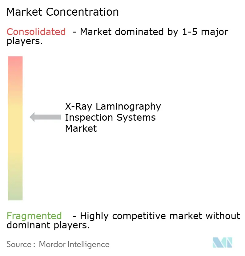
| Market Concentration | Medium |
Major Players *Disclaimer: Major Players sorted in no particular order Image © Mordor Intelligence. Reuse requires attribution under CC BY 4.0. | |
X-Ray Laminography Inspection Systems Market Analysis by Mordor Intelligence
The X-ray laminography inspection systems market size was valued at USD 87.36 million in 2025, is estimated to reach USD 96.62 million in 2026, and is forecast to reach USD 158.69 million by 2031, at a CAGR of 10.61% during the forecast period 2026-2031. Demand is shifting from laboratory failure analysis to production inspection as chiplets, high-bandwidth memory, and hybrid bonding make hidden defects harder to detect with optical tools or 2D X-ray systems. The X-ray laminography inspection systems market benefits when manufacturers need to inspect large, flat samples without removing them from their carriers. Domestic semiconductor projects in North America and Europe also expand the installed base, requiring qualified inspection equipment. Suppliers are placing greater emphasis on reconstruction software, automated defect recognition, and factory connectivity because these functions reduce the time between scanning and a production decision. Capital intensity, validation requirements, and the trade-off between resolution, field of view, and throughput will continue to limit adoption at smaller facilities.
Key Report Takeaways
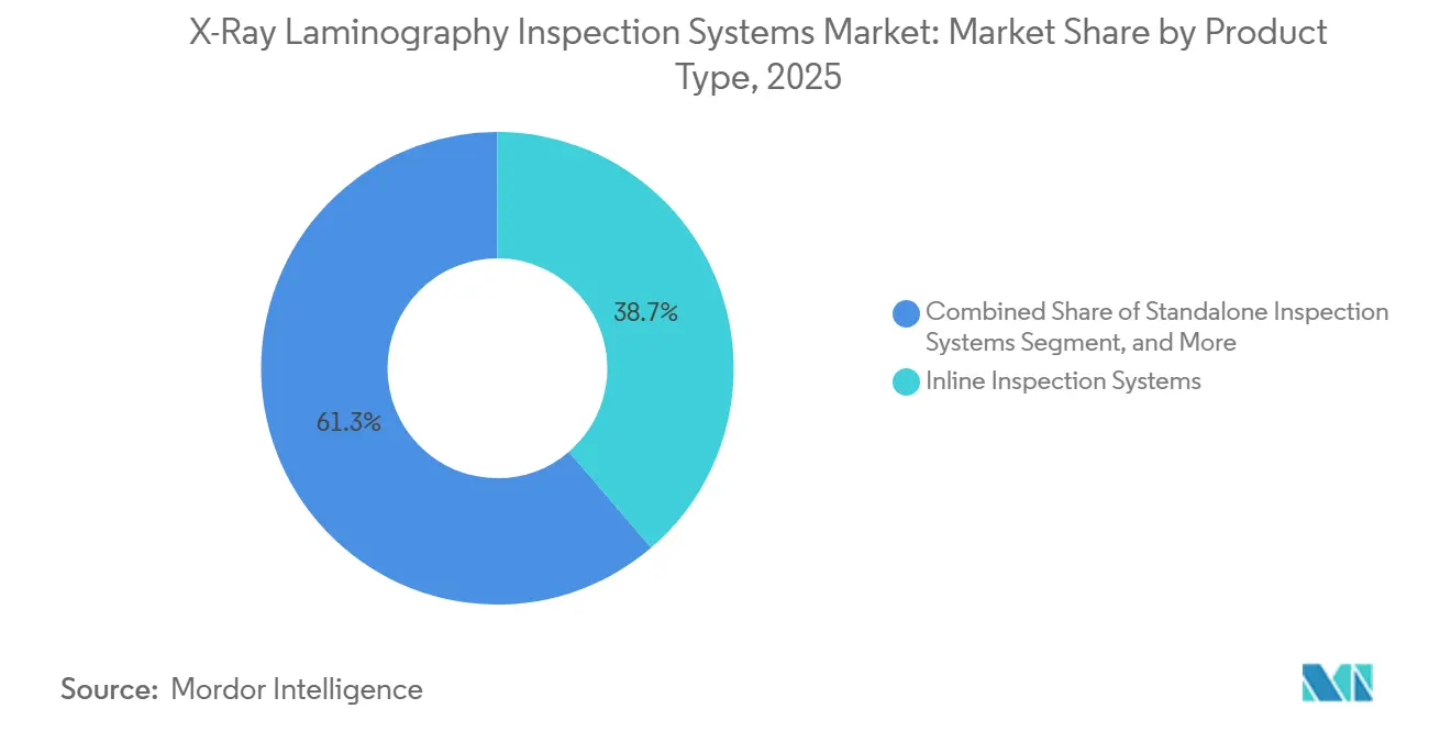
- By product type, inline inspection systems held 38.73% of revenue share in 2025 and are projected to expand at a 12.37% CAGR through 2031.
- In terms of technology, computed laminography accounted for 48.67% of revenue share in 2025 and is projected to expand at a 12.83% CAGR through 2031.
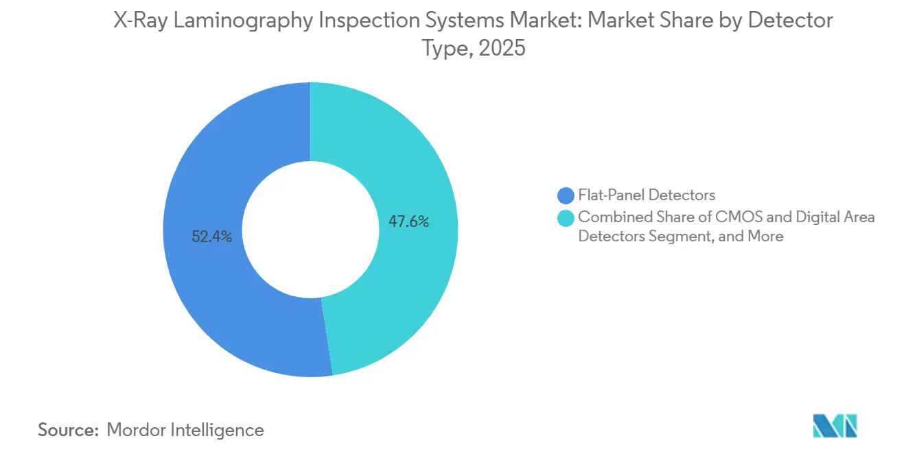
- By detector type, flat-panel detectors accounted for 52.43% of revenue share in 2025, while high-resolution photon-counting detectors are projected to expand at a 13.63% CAGR through 2031.
- By end-user industry, semiconductor and electronics held 34.83% of revenue share in 2025, while automotive and electric vehicles are projected to expand at a 13.97% CAGR through 2031.
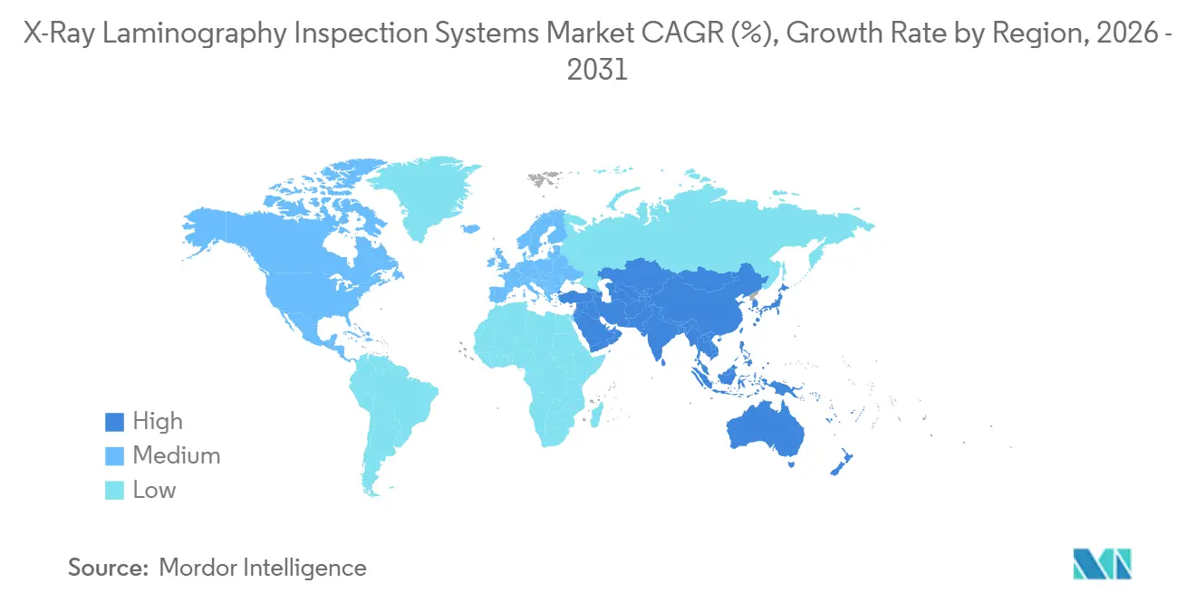
- By geography, Asia-Pacific held 42.76% of the X-ray laminography inspection systems market share in 2025 and is projected to expand at a 13.17% CAGR through 2031.
Key Report Takeaways
| Segmentation | Segment | Metric | Year | Value |
|---|---|---|---|---|
| By Product Type | Inline Inspection Systems | Market Share | 2025 | 38.73% |
| By Product Type | Inline Inspection Systems | CAGR | 2031 | 12.37% |
| By Technology | Computed Laminography | Market Share | 2025 | 48.67% |
| By Technology | Computed Laminography | CAGR | 2031 | 12.83% |
| By Detector Type | Flat-Panel Detectors | Market Share | 2025 | 52.43% |
| By Detector Type | High-Resolution Photon-Counting Detectors | CAGR | 2031 | 13.63% |
| By End-User Industry | Semiconductor and Electronics | Market Share | 2025 | 34.83% |
| By End-User Industry | Automotive and Electric Vehicles | CAGR | 2031 | 13.97% |
| By Geography | Asia-Pacific | Market Share | 2025 | 42.76% |
| By Geography | Asia-Pacific | CAGR | 2031 | 13.17% |
| Source: Mordor Intelligence | ||||
Note: Market size and forecast figures in this report are generated using Mordor Intelligence’s proprietary estimation framework, updated with the latest available data and insights as of January 2026.
Global X-Ray Laminography Inspection Systems Market Trends and Insights
Drivers Impact Analysis*
| Driver | (~) % Impact on CAGR Forecast | Geographic Relevance | Impact Timeline |
|---|---|---|---|
| Advanced Packaging and Heterogeneous Integration | +2.5% | Global, strongest in Asia-Pacific and North America | Long term (≥ 4 years) |
| Inline Wafer-Level Inspection for 300 mm Advanced Packaging | +1.8% | Asia-Pacific core, North America growing | Long term (≥ 4 years) |
| High-Density Double-Sided PCBs and Hidden Solder-Joint Defects | +1.5% | Global, concentrated in Asia-Pacific and Europe | Medium term (2-4 years) |
| AI-Assisted Reconstruction and Automated Defect Recognition | +1.2% | Global | Medium term (2-4 years) |
| EV Battery and Power-Electronics Reliability Requirements | +0.9% | North America, Europe, China | Medium term (2-4 years) |
| Domestic Semiconductor Capacity Expansion | +0.8% | North America, Europe | Short term (≤ 2 years) |
| Source: Mordor Intelligence | |||
Advanced Packaging and Heterogeneous Integration Drive Volumetric Inspection Demand
The move from monolithic dies to chiplet designs is a central driver for the X-ray laminography inspection systems market. Chiplet stacks bring together materials with different thermal expansion behavior, which can create interfacial voids, delamination, and microcracks that affect reliability. Computed laminography can inspect full PCBs and advanced chiplets with image quality comparable to 3D X-ray microscopy while enabling faster acquisition on larger planar samples. The flat-sample geometry also supports non-destructive inspection of 300 mm wafers carrying stacked high-bandwidth memory modules and fine interconnects.[1] Each additional chiplet supplier can introduce another point at which inspection is needed throughout wafer processing and package assembly. Research on hybrid copper bonding found that high-resolution 3D X-ray imaging, including laminography, enabled non-destructive 3D analysis of these structures.
Inline Wafer-Level Inspection for 300 mm Advanced Packaging Enables Defect-Cost Reduction
Inline systems support earlier identification of bonding defects before packaging, testing, and module assembly, and add value to defective parts. Conventional failure-analysis systems can take hours to scan a 300 mm wafer, which restricts their use in process control. The X-ray laminography inspection systems market is therefore shifting toward tools that combine laminographic geometry, iterative reconstruction, and automated wafer handling. For tool buyers, this changes the decision from buying an imaging device to validating a production asset that must operate reliably beside handling, metrology, and quality systems. ZEISS positions its NLX platform for inline 3D X-ray laminography at the 300 mm wafer level within wafer-fab workflows. Rapid wafer-level inspection research also showed that AI-assisted reconstruction can shorten laminographic scan times without dependence on lateral sample size. SEMI S2 and S8 safety requirements, F47 voltage-sag requirements, and SECS/GEM interfaces remain important qualification conditions for the deployment of fully automated fabs.
High-Density Double-Sided PCBs and Hidden Solder-Joint Defects Sustain PCB Inspection Demand
Dense double-sided PCBs used in AI servers, 5G base stations, and EV inverters can obscure bottom-side solder joints in 2D X-ray images. Computed laminography separates planar layers, helping inspectors identify voids, bridges, and shorts that overlap in conventional projections. A 2025 review described the technique across PCB, microelectronic, and other planar applications, including its reconstruction methods and operating limits. Mode-switchable computed laminography can also be configured for plate-like objects with different thicknesses, which broadens use across PCB substrates SCIENCEDIRECT.COM. Saki developed its 3Xi-ZS1EX system for ultra-large PCB inspection, combining 3D CT, AI-based noise reduction, and automatic board-warp correction. Larger boards and rising layer counts increase the value of non-destructive layer separation in electronics assembly. The X-ray laminography inspection systems market can therefore serve applications where conventional projection images provide insufficient separation between densely packed features.
AI-Assisted Reconstruction and Automated Defect Recognition Close the Throughput Gap
A laminography scan can produce gigabytes of volumetric data, and conventional reconstruction can exceed the cycle time available on production lines. Deep-learning restoration can recover image quality from shorter exposures and help make rapid acquisition more practical for wafer-level packaging inspection. Viscom introduced vAI ProVision at Productronica 2025 to enable the creation of 3D AXI inspection programs in minutes rather than days. The X-ray laminography inspection systems market gains value when automated recognition turns raw images into process feedback rather than a stand-alone inspection record. A customized segment-anything model trained on PCB computed laminography images improved component detection compared with generic vision models. Suppliers with production-image libraries can use that data to improve application-specific models and support recurring software differentiation. In the X-ray laminography inspection systems market, this puts practical value on installed-base data, recipe experience, and integration support, as well as image resolution.
Restraints Impact Analysis*
| Restraint | (~) % Impact on CAGR Forecast | Geographic Relevance | Impact Timeline |
|---|---|---|---|
| High Capital Cost and Long Qualification Cycles | -1.9% | Global, most pronounced in price-sensitive Asia-Pacific | Long term (≥ 4 years) |
| Resolution, Field of View, and Throughput Trade-Offs | -1.2% | Global | Long term (≥ 4 years) |
| Shortage of Skilled X-Ray and Advanced-Packaging Engineers | -0.8% | Global | Medium term (2-4 years) |
| Fragmented Performance Standards and Data-Interpretation Practices | -0.5% | Global | Medium term (2-4 years) |
| Source: Mordor Intelligence | |||
High Capital Cost and Long Qualification Cycles Limit Addressable Market Depth
A 300 mm inline computed laminography system can require a large capital commitment, which is difficult for smaller OSATs and contract PCB assemblers to justify. Semiconductor fabs also run split lots, repeatability tests, and reviews by engineering and quality teams before accepting a new process-control tool. These steps can add 12 to 18 months before a system begins routine production use. Consequently, the X-ray laminography inspection systems market reaches large IDMs and major OSATs earlier than smaller packaging providers. Maintenance, recipe updates, and detector calibration also require personnel with advanced expertise in packaging and X-ray. CHIPS Act programs can help qualifying domestic manufacturers address access costs, although the adoption gap between large and small facilities remains.
Resolution, Field of View, and Throughput Trade-Offs Constrain Standardization
Laminography provides strong lateral resolution on large flat samples, but its geometry creates a trade-off among spatial resolution, field of view, and acquisition time. High-resolution work on large planar samples can require systems that combine CT and laminography, adding mechanical complexity and cost.[2] Photon-counting detectors can lower noise and increase frame rates, but their cost limits use to higher-value inspection applications. A 2025 study reported 1-second battery-cell-overhang scans using photon-counting detectors and high-brightness MetalJet X-ray sources. Reconstruction artifacts, including missing-cone effects and beam hardening, still need substantial computational correction. Each new application can therefore need a custom inspection recipe until common operating standards become more established.
*Our forecasts treat driver/restraint impacts as directional, not additive. The impact forecasts reflect baseline growth, mix effects, and variable interactions.
Segment Analysis
By Product Type: Inline Systems Lead Production Deployment
Inline inspection systems are projected to expand at a 12.37% CAGR through 2031, the fastest rate among product types in the X-ray laminography inspection systems market. Inline inspection systems accounted for 38.73% of revenue in 2025, confirming their position as the leading product type in production-oriented deployments. Earlier detection of a void during die attachment prevents the need to perform later underfill, molding, singulation, and testing for a defective unit. Standalone inspection systems remain useful in failure analysis and process development, where flexible sample handling and imaging depth matter more than cycle time. They support the inspection of coupons and new package structures introduced at each process node.
Near-line systems provide adjacent production cells with access to shared equipment without the factory interfaces required for a fully inline tool. Laboratory and failure-analysis systems serve R&D work that needs high resolution across intact wafers and chiplet assemblies. Sigray describes its Apex-Hybrid platform as combining orthogonal CT and precision-angle laminography for non-destructive analysis of complex semiconductor and electronics samples. The X-ray laminography inspection systems industry uses these systems to identify regions of interest before targeted cross-sectioning. Fully inline tools have a higher barrier to entry because they must meet cleanroom safety and automation requirements. This distinction preserves a role for near-line and laboratory configurations even as production automation increases. The X-ray laminography inspection systems market needs these configurations because process development teams often need flexibility before a recipe is stable enough for factory automation.

By Technology: Computed Laminography Holds the Leading Position
Computed laminography held 48.67% of the X-ray laminography inspection systems market share in 2025. Its position reflects compatibility with iterative, model-based, and AI-supported reconstruction that can improve image quality from the same projection data. Computed laminography is projected to expand at a 12.83% CAGR through 2031, reflecting the production requirement that supports software-led reconstruction. It also enables quantitative 3D measurement of void volume and solder-bump coplanarity. A 2025 scientific review identified its broad applicability across varying sample sizes, materials, and geometries. Facilities with established equipment can upgrade from conventional approaches to access reconstruction improvements without replacing every mechanical element.
Digital laminography remains relevant for high-throughput PCB lines where speed and lower acquisition cost are more important than isotropic voxel reconstruction. Hybrid tools that combine computed laminography and CT provide failure-analysis laboratories with greater flexibility across sample types. Sigray's Apex-Hybrid product is designed for this combined inspection approach. Conventional laminography continues to support lower-resolution industrial, energy, and aerospace testing. In these applications, simpler gantry designs and flat-panel detectors can meet imaging needs at a lower capital cost. The X-ray laminography inspection systems industry, therefore, retains multiple technology paths rather than adopting a single universal configuration.
By Detector Type: Flat-Panel Detectors Support Volume Deployments
Flat-panel detectors held 52.43% of the X-ray laminography inspection systems market share in 2025. Their large active areas and compatibility with cone-beam geometry support inline and near-line systems used for PCBs, automotive assemblies, and industrial parts. Their cost per pixel makes them a common choice where operating cost is a greater procurement factor than peak imaging performance. CMOS and digital area detectors offer faster frame rates and smaller pixel pitches for flexible production settings. A 2025 dataset from Lappeenranta-Lahti University of Technology demonstrated cone-beam computed laminography of a keyboard circuit board using flat-panel detector configurations at 45° and 60° tilt angles.
High-resolution photon-counting detectors are projected to expand at a 13.63% CAGR through 2031. Direct-conversion sensors can reduce scintillator-related blur and readout noise, enabling shorter exposures for demanding applications. The 1-second battery overhang scan demonstrated in 2025 shows why these detectors are relevant to high-throughput EV production. Photon-counting architectures can provide energy-sensitive imaging data that conventional flat-panel systems do not. High sensor-material and ASIC costs remain a constraint, although larger semiconductor and battery inspection volumes could improve cost economics over time. The X-ray laminography inspection systems market will still require suppliers to show that higher detector performance improves yield, throughput, or both.
By End-User Industry: Semiconductor and Electronics Anchors Demand
Semiconductor and electronics held 34.83% of the X-ray laminography inspection systems market share in 2025. Advanced packaging, including 2.5D and 3D IC designs, chip-on-wafer-on-substrate, and hybrid bonding, is the most demanding use case because buried connections need 3D inspection. High-resolution 3D X-ray imaging was found to enable non-destructive analysis of hybrid copper bonding structures. Consumer electronics and appliances also require inspection of dense flexible substrates and radio-frequency modules. Aerospace and defense applications remain steady because flight-control electronics and power conversion units operate under strict qualification expectations.
Automotive and electric vehicles are projected to expand at a 13.97% CAGR through 2031, the fastest end-user rate. Battery manufacturers are adding inline X-ray inspection to electrode stacking and cell assembly processes, while power-electronics makers use it for inverter assemblies. An ASNT paper in 2026 reported that inline CT and AI-based defect recognition were moving into production battery quality gates, including commercial use on 46-series cylindrical cell lines. The thicker electrodes and tighter overhang tolerances of the 46-series format require greater penetration, coverage, and throughput than earlier systems. Healthcare, energy and power, and industrial machinery are smaller users, with applications in implants, power modules, switchgear, and related assemblies.
Geography Analysis
Asia-Pacific held 42.76% of the X-ray laminography inspection systems market share in 2025 and is projected to expand at a 13.17% CAGR through 2031. China, South Korea, Japan, Taiwan, and Southeast Asia combine advanced packaging fabs, OSATs, and PCB manufacturing at a scale unmatched elsewhere. China has supported domestic inspection infrastructure, alongside semiconductor fab construction and equipment localization efforts, since 2024. Japan remains both a technology supplier and an end market for advanced inspection tools. Saki developed an automated X-ray inspection system for ultra-large PCBs with a 1.6× faster takt time than its previous model.
South Korean logic and memory manufacturers are investing in high-bandwidth memory and advanced packaging for AI accelerators. This activity supports demand for precision laminography at the 300 mm wafer level. India and Southeast Asia are adding packaging and test capacity as supply chains diversify. Those facilities create medium-term demand for inspection equipment and qualified service support. The X-ray laminography inspection systems market in the region also benefits from the close relationship between electronics assembly and component suppliers.
North America held the second-largest geographic share in 2025, supported by aerospace, defense, and a rising domestic fab pipeline. New semiconductor facilities will need qualified inspection equipment during installation and process qualification. Automotive OEMs and Tier-1 suppliers also use inline X-ray systems for EV battery modules and inverter assemblies. Canada and Mexico primarily support contract electronics manufacturing, where medium-complexity PCB inspection is the main use case. Europe is the third-largest region and is home to major inspection system suppliers, including ZEISS, Comet Yxlon, and Viscom. ZEISS introduced VersaXRM 5 Insight in September 2026, combining hybrid 3D X-ray imaging with AI-assisted reconstruction for industrial and research workflows. Germany also supports demand from automotive power-electronics assembly and defense electronics, while South America, the Middle East, and Africa are served mainly by offline aerospace and industrial inspection.
Competitive Landscape
The X-ray laminography inspection systems market is moderately concentrated at the premium end, where Comet Yxlon, ZEISS, Nikon Corporation, and Waygate Technologies compete across advanced packaging, automotive, and industrial inspection. A broader group of regional and application-specific suppliers includes Viscom, Saki Corporation, ViTrox Corporation, Omron Corporation, Shimadzu Corporation, and Unicomp Technology. This mix creates a concentrated high-performance tier and a more fragmented mid-market. The X-ray laminography inspection systems industry increasingly differentiates equipment through reconstruction software, automation, and defect-recognition tools rather than tube voltage or detector specifications alone. These software functions can make a tool more useful within a customer's existing quality workflow.
Viscom introduced vAI ProVision in 2025 to reduce the time to generate 3D AXI programs from days to minutes.[3] ZEISS introduced VersaXRM 5 Insight in 2026 with AI-assisted reconstruction and a new detector architecture. Nikon added a low-dose collimator, ESD safety upgrades, and a high-contrast filter to its XT V Series X-ray and CT systems in 2025. These moves address needs in semiconductor inspection, radiation-sensitive devices, and complex component imaging. Patent positions in precision-angle laminography, reconstruction methods, and nanofocus X-ray sources also support barriers in the highest-resolution applications.
Opportunities remain in panel-level packaging because larger substrates have not yet produced a standard inspection configuration. Suppliers that qualify as reliable tools for these formats could establish supply relationships as panel-level packaging moves beyond pilot work. Energy-storage inspection at the cell-stack and module level also leaves room for focused systems that address high throughput and complex geometry. ViTrox received the 2026 Circuits Assembly NPI Award for its compact V810Ai QX1 3D AXI design. Compact equipment can help smaller suppliers compete in facilities with limited floor space. The market structure supports competition based on application fit, validated integration, and software capability rather than a single hardware standard. The X-ray laminography inspection systems market also rewards suppliers that can support qualification work after installation, since buyers need repeatable performance before accepting a new inspection step.
X-Ray Laminography Inspection Systems Industry Leaders
-
Comet Technologies Germany GmbH
-
Carl Zeiss AG
-
Nikon Corporation
-
Nordson Corporation
-
Sigray, Inc.
- *Disclaimer: Major Players sorted in no particular order
Recent Industry Developments
- September 2026: ZEISS introduced the VersaXRM 5 Insight, a hybrid 3D X-ray microscope combining laboratory X-ray microscopy and microCT with AI-assisted reconstruction and a flat-panel/Resolution-at-a-Distance detector architecture, enabling multi-scale non-destructive imaging from 70 µm full-cell EV battery scans to 0.8 µm/voxel semiconductor package interconnects. The system broadened ZEISS's reach into high-throughput materials research and semiconductor failure-analysis workflows and targeted industrial inspection, semiconductor/electronics quality assurance, and life sciences.
- September 2026: Saki Corporation announced the development of the 3Xi-ZS1EX automated X-ray inspection system for ultra-large PCBs, targeting AI data-center board inspection. The system delivered 1.6× faster takt time than the previous model, incorporated 3D CT inspection with AI-driven noise reduction, and featured automatic PCB-warp correction. Order intake was scheduled to begin in October 2026.
- September 2026: Comet launched the HP/15 minifocus X-ray tube, a redesigned successor to the HP/11, optimized for digital detectors, inline inspection, and CT workflows. The HP/15 featured dual thermally separated focal spots for improved dose homogeneity and simplified integration into computed laminography and CT systems, targeting inline inspection and advanced packaging applications.
- May 2026: Comet Yxlon introduced the High Density Power Target upgrade for its 225 kV X-ray tubes in the FF35 CT and FF85 CT systems, doubling available power density at smaller focal spot sizes and enabling faster CT and laminography inspection without sacrificing resolution, with application to advanced semiconductor packaging and complex manufacturing assemblies.
Global X-Ray Laminography Inspection Systems Market Report Scope
The X-Ray Laminography Inspection Systems Market comprises revenue generated from the sale, integration, software, maintenance, and inspection services associated with industrial X-ray laminography systems used to produce depth-resolved or slice-based images of internal features in components, assemblies, and materials. These systems use specialized X-ray sources, objects, and detector geometries, often involving limited-angle, oblique-axis, or synchronized movement, to focus on selected planes while suppressing or blurring information from surrounding layers. This makes laminography particularly suitable for flat, multilayer, or densely assembled objects such as printed circuit boards, semiconductor packages, solder joints, batteries, and composite structures.
The X-Ray Laminography Inspection Systems Market Report is Segmented by Product Type (Standalone Inspection Systems, Inline Inspection Systems, Near-Line Inspection Systems, and Laboratory and Failure-Analysis Systems), Technology (Computed Laminography, Digital Laminography, and Conventional Laminography), Detector Type (Flat-Panel Detectors, CMOS and Digital Area Detectors, and High-Resolution Photon-Counting Detectors), End-User Industry (Semiconductor and Electronics, Automotive and Electric Vehicles, Energy and Power, Aerospace and Defense, Healthcare, Industrial and Machinery Manufacturing, Consumer Electronics and Appliances, and Other End-User Industries), and Geography (North America, South America, Europe, Asia-Pacific, and Middle East and Africa). Market Forecasts are Provided in Terms of Value (USD).
| Standalone Inspection Systems |
| Inline Inspection Systems |
| Near-Line Inspection Systems |
| Laboratory and Failure-Analysis Systems |
| Computed Laminography |
| Digital Laminography |
| Conventional Laminography |
| Flat-Panel Detectors |
| CMOS and Digital Area Detectors |
| High-Resolution Photon-Counting Detectors |
| Semiconductor and Electronics |
| Automotive and Electric Vehicles |
| Energy and Power |
| Aerospace and Defense |
| Healthcare |
| Industrial and Machinery Manufacturing |
| Consumer Electronics and Appliances |
| Other End-User Industries |
| North America | United States | |
| Canada | ||
| Mexico | ||
| South America | Brazil | |
| Argentina | ||
| Rest of South America | ||
| Europe | Germany | |
| United Kingdom | ||
| France | ||
| Italy | ||
| Spain | ||
| Rest of Europe | ||
| Asia-Pacific | China | |
| Japan | ||
| India | ||
| South Korea | ||
| ASEAN | ||
| Rest of Asia-Pacific | ||
| Middle East and Africa | Middle East | Saudi Arabia |
| United Arab Emirates | ||
| Turkey | ||
| Rest of the Middle East | ||
| Africa | South Africa | |
| Nigeria | ||
| Rest of Africa | ||
| By Product Type | Standalone Inspection Systems | ||
| Inline Inspection Systems | |||
| Near-Line Inspection Systems | |||
| Laboratory and Failure-Analysis Systems | |||
| By Technology | Computed Laminography | ||
| Digital Laminography | |||
| Conventional Laminography | |||
| By Detector Type | Flat-Panel Detectors | ||
| CMOS and Digital Area Detectors | |||
| High-Resolution Photon-Counting Detectors | |||
| By End-User Industry | Semiconductor and Electronics | ||
| Automotive and Electric Vehicles | |||
| Energy and Power | |||
| Aerospace and Defense | |||
| Healthcare | |||
| Industrial and Machinery Manufacturing | |||
| Consumer Electronics and Appliances | |||
| Other End-User Industries | |||
| By Geography | North America | United States | |
| Canada | |||
| Mexico | |||
| South America | Brazil | ||
| Argentina | |||
| Rest of South America | |||
| Europe | Germany | ||
| United Kingdom | |||
| France | |||
| Italy | |||
| Spain | |||
| Rest of Europe | |||
| Asia-Pacific | China | ||
| Japan | |||
| India | |||
| South Korea | |||
| ASEAN | |||
| Rest of Asia-Pacific | |||
| Middle East and Africa | Middle East | Saudi Arabia | |
| United Arab Emirates | |||
| Turkey | |||
| Rest of the Middle East | |||
| Africa | South Africa | ||
| Nigeria | |||
| Rest of Africa | |||
Key Questions Answered in the Report
What is the X-ray laminography inspection systems market size?
The X-ray laminography inspection systems market size is estimated at USD 96.62 million in 2026 and is forecast to reach USD 158.69 million by 2031 at a 10.61% CAGR.
Which product type is expanding fastest in X-ray laminography inspection systems?
Inline inspection systems are projected to expand at a 12.37% CAGR through 2031 as fabs and OSATs add volumetric inspection to production lines.
Why is computed laminography important for semiconductor packaging?
It held 48.67% of revenue share in 2025 and supports 3D inspection of buried interconnects, voids, and hybrid-bonding structures.
Which detector type leads X-ray laminography deployments?
Flat-panel detectors held 52.43% of revenue share in 2025, while photon-counting detectors are projected to record the fastest detector growth at a 13.63% CAGR.
Which end-user application is growing fastest?
Automotive and electric vehicles are projected to expand at a 13.97% CAGR through 2031, supported by battery-cell and power-electronics inspection needs.
Which region leads demand for X-ray laminography inspection systems?
Asia-Pacific held 42.76% of revenue share in 2025 and is projected to expand at a 13.17% CAGR through 2031.