Sputter Coating Market Size and Share
Market Overview
| Study Period | 2019 - 2030 |
|---|---|
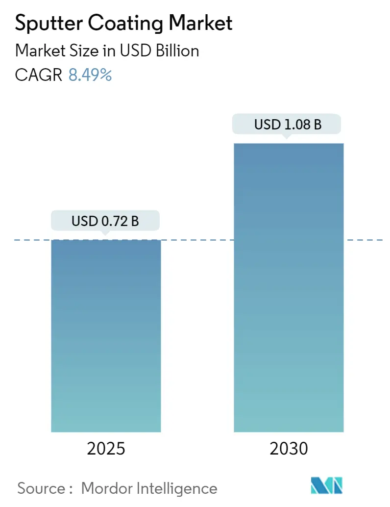
| Market Size (2025) | USD 0.72 Billion |
| Market Size (2030) | USD 1.08 Billion |
| Growth Rate (2025 - 2030) | 8.49% CAGR |
| Fastest Growing Market | Asia Pacific |
| Largest Market | North America |
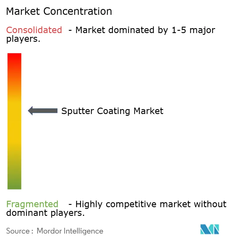
| Market Concentration | Medium |
Major Players *Disclaimer: Major Players sorted in no particular order Image © Mordor Intelligence. Reuse requires attribution under CC BY 4.0. | |
Sputter Coating Market Analysis by Mordor Intelligence
The sputter coating market size stands at USD 721.83 million in 2025 and is forecast to reach USD 1,084.77 million by 2030, advancing at an 8.49% CAGR over 2025-2030. The upturn is propelled by HiPIMS adoption, VOC-free processing mandates, and widening thin-film electronics demand. Equipment suppliers are scaling power supplies and chamber designs to support larger substrates, while target manufacturers are expanding rare-earth capacity to serve quantum, battery, and sensor applications. Concurrently, flexible device production, low-E architectural glazing, and heterojunction solar cells expand the addressable opportunity set. Competitive intensity remains moderate as global majors use integrated hardware-and-materials offerings to defend share, but niche specialists are capturing value in exotic targets and AI-driven process control solutions.
Key Report Takeaways
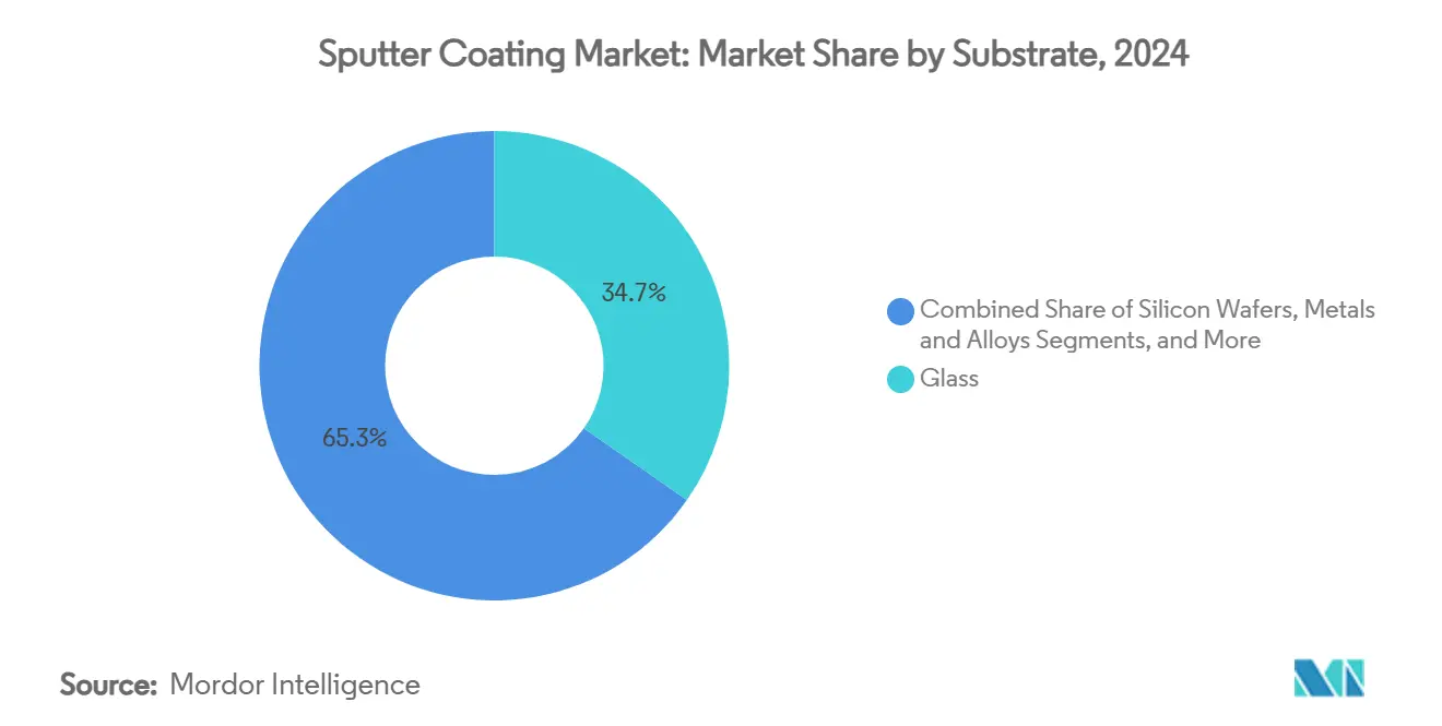
- By substrate, glass held 34.7 % of the sputter coating market share in 2024, whereas polymers/plastics posted the fastest 9.72 % CAGR through 2030.
- By target material, pure metals accounted for a 42.5 % share of the sputter coating market size in 2024, while rare-earth & exotic compounds are poised to expand at a 9.92 % CAGR.
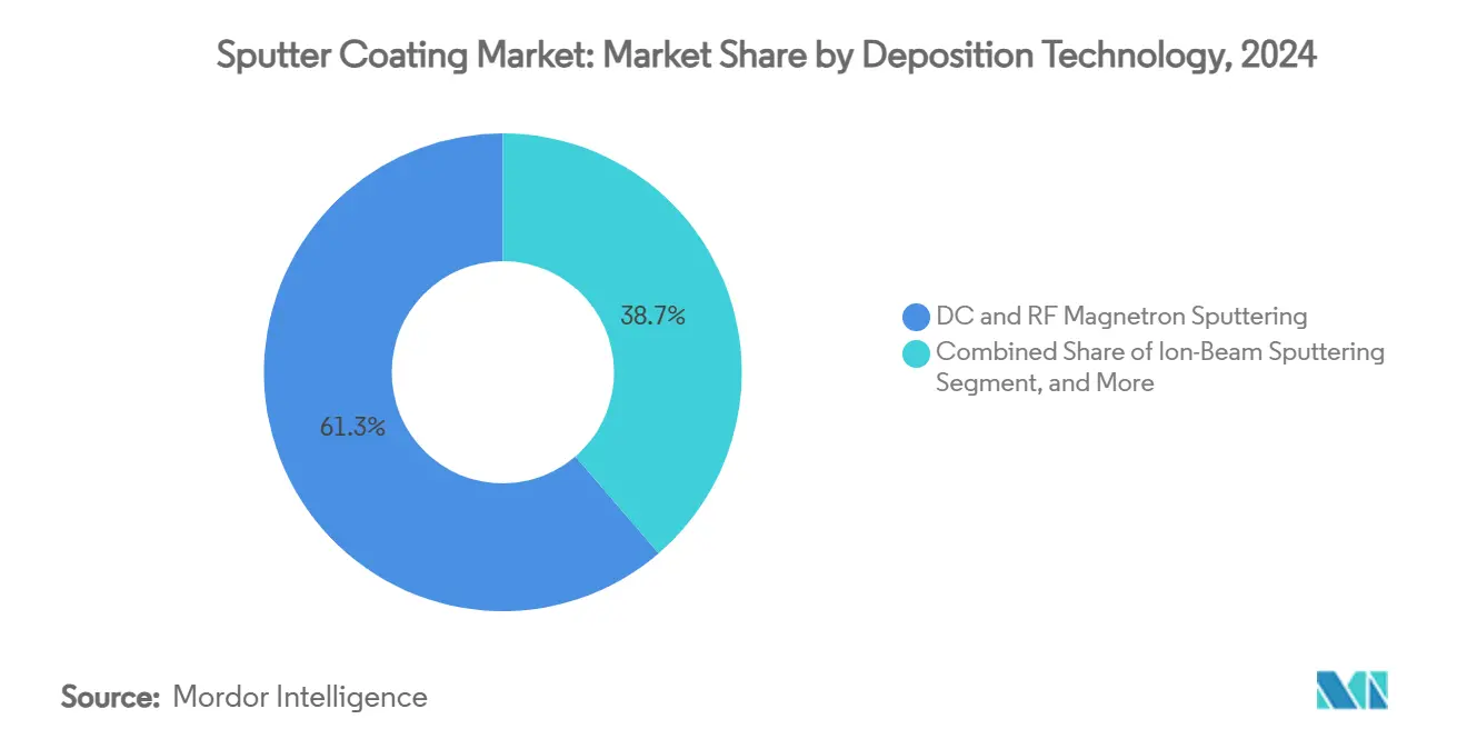
- By deposition technology, DC + RF magnetron commanded 61.3 % of the sputter coating market share in 2024; HiPIMS is projected to register an 11.32 % CAGR to 2030.
- By end-use, electronics & semiconductors led with 48.1 % revenue share in 2024; medical devices represent the fastest-growing segment at 10.93 % CAGR.
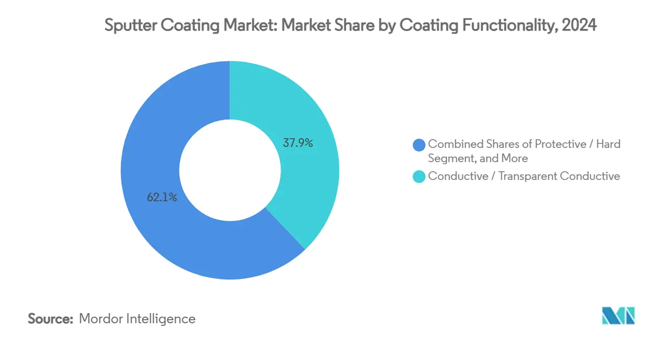
- By coating functionality, Conductive and transparent conductive films owned 37.9 % share in 2024, while Barrier/diffusion layers posted a 10.52 % CAGR to 2030.
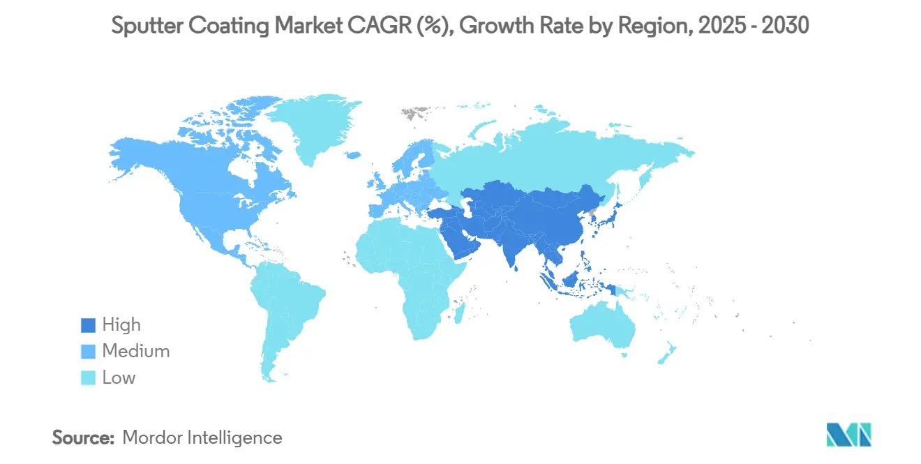
- By geography, Asia-Pacific dominated at 38.4 % share in 2024 and is anticipated to grow at an 11.71 % CAGR through 2030.
Global Sputter Coating Market Trends and Insights
Drivers Impact Analysis*
| Driver | (~) % Impact on CAGR Forecast | Geographic Relevance | Impact Timeline |
|---|---|---|---|
| Rising demand for thin-film electronics & flat-panel displays | +1.80% | APAC core, spill-over to North America | Medium term (2-4 years) |
| Acceleration of thin-film solar PV installations | +1.40% | Global, with concentration in APAC & Europe | Long term (≥ 4 years) |
| Expansion in architectural & optical low-E glass coatings | +1.20% | North America & EU, emerging in APAC | Medium term (2-4 years) |
| Regulations pushing VOC-free, PVD-based coatings | +1.00% | EU & North America, expanding globally | Short term (≤ 2 years) |
| Emergence of HiPIMS enabling high-value functional films | +0.90% | Global, led by advanced manufacturing regions | Long term (≥ 4 years) |
| Uptake of sputter-coated flexible & wearable medical sensors | +0.70% | North America & EU, with APAC manufacturing | Medium term (2-4 years) |
| Source: Mordor Intelligence | |||
Rising Demand for Thin-Film Electronics & Flat-Panel Displays
Demand for ultra-high-resolution displays is forcing deposition uniformity at nanometer tolerances, prompting tool upgrades such as Tokyo Electron’s Ulucus LX platform that delivers atomic-level repeatability. Flexible phones and OLED TVs require sputter-deposited barrier layers that survive millions of bend cycles, steering substrate makers toward polymer sheets. End-users deploy AI-driven feedback loops for real-time plasma tuning, lifting yield, and lowering scrap. Larger glass sheets-Gen 10.5 and beyond-necessitate multi-cathode layouts, keeping equipment ASPs elevated. These shifts collectively funnel value into the sputter coating market as downstream brands demand reliability and production scale.
Acceleration of Thin-Film Solar PV Installations
Record utility-scale buildouts are boosting consumption of transparent conductive oxides. Heterojunction and tandem perovskite-silicon cells require sequential sputtered layers to minimize optical loss [1]Journal of Physics: Conference Series, “Magnetron Sputtering and Electron Beam Evaporation Systems for Pure Boron Thin Film Coatings,” IOPSCIENCE.IOP.ORG. Suppliers are launching 2 m-plus inline systems with in-situ ellipsometry to guarantee sheet-resistance specifications. Indium usage constraints spur R&D into aluminum-doped zinc oxide targets, widening material diversity. Government incentives in China, India, and the EU further accelerate capex cycles, enhancing visibility for tool vendors over a long-term horizon.
Expansion in Architectural & Optical Low-E Glass Coatings
Triple-silver stacks incorporating up to 15 layers now define premium façades, demanding line speeds above 4 m/min while holding emissivity tolerances below 0.02. European retrofit mandates and U.S. energy-code updates stimulate capacity additions in tempering lines that integrate inline magnetron sputtering. Quality-assurance teams deploy laser scatterometry to detect nanoscale voids, pushing suppliers toward closed-loop cathode power modulation. Electrochromic glass commercial pilots also use sputtered ion-storage layers, diversifying end applications.
Regulations Pushing VOC-Free, PVD-Based Coatings
The EU Industrial Emissions Directive caps plant-wide solvent emissions at 20 mg Nm³, accelerating the shift from hexavalent chrome plating toward tungsten-carbide PVD alternatives in aerospace and automotive parts[2]Advanced Manufacturing, “PVD Coatings as Replacement for Hard Chrome on Components,” ADVANCEDMANUFACTURING.ORG. Early movers secure compliance cost advantages and marketing claims, driving retrofits of legacy lines with multi-cathode chambers. Hybrid wet-PVD lines combining etch, plating, and sputter steps inside one cluster are emerging to ease change-management and operator training.
Restraints Impact Analysis*
| Restraint | (~) % Impact on CAGR Forecast | Geographic Relevance | Impact Timeline |
|---|---|---|---|
| High capital cost of vacuum sputter equipment | -1.10% | Global, particularly impacting emerging markets | Short term (≤ 2 years) |
| Growing competition from ALD & CVD techniques | -0.80% | Advanced manufacturing regions, APAC & North America | Medium term (2-4 years) |
| Supply-chain risk for rare-earth / indium-based targets | -0.60% | Global, with acute impact in APAC manufacturing | Long term (≥ 4 years) |
| Thermal management limits on ultrathick power-device films | -0.40% | Semiconductor manufacturing regions globally | Medium term (2-4 years) |
| Source: Mordor Intelligence | |||
High Capital Cost of Vacuum Sputter Equipment
Multi-chamber systems surpass USD 5 million, and fab buildouts exceed USD 10 million after clean-room fit-out, utilities, and training[3]ASME Digital Collection, “Thermal Analysis and Control for Sputtering Deposition of High-Tc Superconducting Films,” ASME.ORG. Depreciation strainsthe balance sheets of small EMS and display firms, especially in Southeast Asia. Preventive-maintenance contracts add 5 % to annual OpEx. Vendors counter with leasing models and modular load-locks that scale with volume, though financing hurdles persist where tech-lending ecosystems are immature.
Growing Competition from ALD & CVD Techniques
ALD’s self-limiting chemistry achieves fully conformal coatings in 3D NAND stacks beyond 200 layers, a niche that sputtering cannot economically cover [4]Applied Materials, “Applied Materials Expands Manufacturing Footprint in India,” APPLIEDMATERIALS.COM. Plasma-enhanced ALD now runs below 80 °C, encroaching on polymer devices. Meanwhile, CVD retains throughput advantages for thick dielectrics. Sputter OEMs respond by bundling integrated ALD modules, but market share erosion in high-aspect-ratio nodes is likely.
*Our forecasts treat driver/restraint impacts as directional, not additive. The impact forecasts reflect baseline growth, mix effects, and variable interactions.
Segment Analysis
By Substrate: Glass Dominance Faces Polymer Challenge
Glass generated 34.7 % of 2024 revenue. Its thermal endurance supports high-power processes up to 600 °C, ensuring adhesion of silver-based low-E stacks. Conversely, polymers post the fastest 9.72 % CAGR as smart-watch faces and HUD windshields proliferate. Larger Gen-8 lines in China raised the sputter coating market size for glass by USD 58 million in 2024. Polymer web coaters tap roll-to-roll economies, shrinking per-square-meter costs. Moisture barrier performance has reached transmission rates below 10⁻⁶ g m⁻² day⁻¹ after ALD-on-PVD hybridization, enabling glucose-patch commercialization. Despite outgassing issues, primers and in-situ plasma treatment are closing adhesion gaps, positioning polymers to chip away at the incumbent.
Ongoing investments by automotive tier-ones in holographic windshields underscore the shift. Zeiss and Hyundai Mobis validated sputter-deposited index-matched stacks on curved PMMA panes for 3-D HUD prototypes, reflecting how polymers unlock lightweight optics without compromising clarity. As recycling regulations bite, glass retains an advantage in circularity, yet bio-based PET films are entering pilot scale, hinting at a more balanced substrate mix by 2030.


By Target Material: Pure Metals Lead While Exotics Accelerate
Pure metals held a 42.5 % share on steady demand for Al, Cu, and Ag cathodes in display backplanes. This dominance anchors consumables revenue streams for OEMs. Still, rare-earth & exotic compounds are projected at 9.92 % CAGR as quantum qubits and Li-metal batteries require YBCO and LiPON targets. The segment added USD 12 million to the sputter coating market size in 2024 on new JX Advanced Metals lines in Arizona.
Composite hot-isostatic-pressed targets lengthen campaign life by 30 %, reducing downtime for costly materials. Recycle-as-a-service contracts now guarantee reclaim rates above 85 %, insulating fabs from price swings. Regulations on conflict minerals spur tracing platforms that tag target batches with blockchain IDs, boosting supply-chain transparency.
By Deposition Technology: Magnetron Dominance, HiPIMS Surge
DC/RF magnetron remained the workhorse, responsible for 61.3 % of 2024 turnover thanks to proven uptime and familiar process kits. Cluster-tool configurations enable sequential layer stacks without a vacuum break, keeping the cost per wafer low. Yet HiPIMS notably posts an 11.32 % CAGR, expanding sputter coating market share in cutting-tool and barrier-metal niches. Recent 6000 A pulsed supplies cut arcing events by 40 %, lifting throughput.
Ion-beam sputtering enjoys footholds in optics, but its sub-1 nm roughness advantage is offset by capital intensity. Reactive sputtering’s share stabilizes as demand for metal-nitride contacts climbs in power semis. Over the horizon, hybrid HiPIMS-ALD modules aim to marry density with conformality, hinting at platform convergence.
By End-Use Industry: Electronics Leadership Challenged by Medical Growth
Electronics & semiconductors delivered 48.1 % revenue in 2024. AI accelerators and 5G RF front-ends require ultra-thin diffusion barriers, keeping fab utilization high. However, medical devices rise at a 10.93 % CAGR, adding USD 6 million incremental revenue in 2024 alone. Chronic-disease monitoring fuels volume for disposable biosensor electrodes, while titanium-nitride heart-valve coatings lengthen device life.
Solar energy sustains momentum as FIT schemes in India extend guaranteed tariffs. Automotive adoption widens, with lidar and battery packs demanding precise coatings. Aerospace seeks erosion-resistant films for compressor blades, validating sputtering’s materials versatility.
By Coating Functionality: Conductive Films Lead, Barrier Growth Accelerates
Conductive and transparent conductive films owned a 37.9 % share in 2024. ITO remains the default for touch panels despite indium pricing swings. Silver-mesh hybrids are entering commercial display volumes, broadening options. Barrier/diffusion layers post a 10.52 % CAGR, reflecting the miniaturization of chip packages and moisture-sensitive batteries. Copper diffusion barriers under 5 nm thickness incorporate TaN/TiN bilayers via HiPIMS, avoiding ALD cycle-time penalties.
Decorative PVD captures automotive trim as OEMs pivot away from chrome. Protective films based on DLC and TiCN grow in drills and dies, leveraging mechanical gains from HiPIMS densification.
Geography Analysis
Asia-Pacific retained 38.4 % of global revenue in 2024 and is projected to grow at an 11.71 % CAGR to 2030. State incentives in China financed ten Gen-8 display fabs in 2024, each integrating >40 cathodes per pane, thereby enlarging the regional sputter coating market size[5]Invest Taiwan, “Japan’s Semiconductor Equipment Industry Policies and Guidelines,” INVESTTAIWAN.NAT.GOV.TW. Japan’s equipment pipeline benefits from yen weakness, lifting export margins for Tokyo Electron and ULVAC. Emerging Indian subsidy schemes under SPECS spur localized tool assembly, shortening lead times by 30 days.
North America ranks second, buoyed by U.S. CHIPS Act grants that underpin fab relocations. Aerospace majors certify tungsten-carbide PVD as a hex-chrome replacement, spurring Midwest job shops to install inline coaters. The medical cluster in Minnesota expands the consumption of noble-metal targets for neural implants. Environmentally stringent states like California push automotive suppliers toward PVD decorative parts, solidifying regional demand.
Europe shows steady uptake. Building codes in Germany and France mandate U-values below 1.0 W m-² K-¹, driving low-E glass retrofits. OEMs in the EU shift to electroless-Ni-P plus PVD hybrid stacks, trimming lifecycle CO₂. Von Ardenne’s Dresden hub shipped record web coaters for BIPV panels in 2024. The continent’s push for circularity catalyzes recycling plants for used cathodes, creating closed-loop material flows and dampening raw-material price shocks.

Competitive Landscape
Global majors-Applied Materials, ULVAC, Tokyo Electron-anchor the market with end-to-end portfolios. Their scale secures priority on semiconductor expansion projects, reinforcing a combined 45 % revenue share. Mid-tier firms such as Oerlikon and Von Ardenne differentiate via application labs and stack design IP for optical and wear coatings. Niche specialists, including Intevac and Mustang Vacuum, carve out roles in HiPIMS and ion-beam segments.
Consolidation accelerates: Seagate’s purchase of Intevac’s tool unit extends vertical integration for HDD media; Integer Holdings’ Precision Coating acquisition seeds captive PVD capacity for medical devices. Toolmakers integrate AI modules that predict end-point and schedule cathode changeovers, lifting OEE by 5 points. Target suppliers roll out take-back programs, bundling metal reclaim with new-target deliveries to lock long-term contracts.
White-space opportunities remain in quantum computing and energy storage, where material recipes are nascent. Start-ups commercialize modular HiPIMS power stacks, offering retrofit paths for legacy chambers. ESG scrutiny heightens, prompting OEMs to publish 2030 net-zero roadmaps and to substitute PFAS-based etchants with Ar-only cleans.
Sputter Coating Industry Leaders
Applied Materials Inc.
ULVAC Inc.
OC Oerlikon Balzers AG
Veeco Instruments Inc.
Bühler Leybold Optics GmbH
- *Disclaimer: Major Players sorted in no particular order

Recent Industry Developments
- January 2025: Applied Materials opened a Bengaluru plant to assemble advanced sputter systems, aiming to localize supply for India-based fabs while de-risking cross-border logistics. The move aligns with the firm’s strategy of footprint diversification and customer-proximity manufacturing.
- November 2024: SCREEN Semiconductor Solutions debuted the SS-3200 wafer scrubber, complementing its sputter portfolio by reducing particle counts prior to barrier deposition, thereby positioning the company for power-device process flows.
- October 2024: Integer Holdings acquired Precision Coating, securing in-house biocompatible PVD capability that shortens medical-device launch cycles and enhances vertical integration.
- September 2024: JX Advanced Metals commissioned a Mesa, Arizona target plant to serve North American logic fabs, mitigating geopolitical supply risk and shortening lead times.


Global Sputter Coating Market Report Scope
| Glass |
| Silicon Wafers |
| Metals & Alloys |
| Polymers / Plastics |
| Ceramics & Others |
| Pure Metals (Al, Cu, Ag, Ti, etc.) |
| Alloys (AlCrN, NiCr, etc.) |
| Oxides (ITO, ZnO, etc.) |
| Nitrides / Carbides |
| Rare-earth & Exotic Compounds |
| DC Magnetron Sputtering |
| RF Magnetron Sputtering |
| Ion-Beam Sputtering |
| Reactive Sputtering |
| HiPIMS |
| Electronics and Semiconductors |
| Solar Power |
| Architectural Glass |
| Automotive |
| Medical Devices |
| Aerospace and Defense |
| Energy Storage |
| Other End-Use Industries (Decorative, Tools) |
| Conductive / Transparent Conductive |
| Optical (AR / HR / Filter) |
| Protective / Hard |
| Decorative |
| Barrier / Diffusion |
| North America | United States | |
| Canada | ||
| Mexico | ||
| South America | Brazil | |
| Rest of South America | ||
| Europe | Germany | |
| United Kingdom | ||
| France | ||
| Rest of Europe | ||
| Asia-Pacific | China | |
| Japan | ||
| Taiwan | ||
| ASEAN (Indonesia, Vietnam, Thailand, Malaysia, Philippines, Singapore) | ||
| Rest of Asia-Pacific | ||
| Middle East and Africa | Middle East | Saudi Arabia |
| United Arab Emirates | ||
| Turkey | ||
| Rest of Middle East | ||
| Africa | South Africa | |
| Egypt | ||
| Rest of Africa | ||
| By Substrate | Glass | ||
| Silicon Wafers | |||
| Metals & Alloys | |||
| Polymers / Plastics | |||
| Ceramics & Others | |||
| By Target Material | Pure Metals (Al, Cu, Ag, Ti, etc.) | ||
| Alloys (AlCrN, NiCr, etc.) | |||
| Oxides (ITO, ZnO, etc.) | |||
| Nitrides / Carbides | |||
| Rare-earth & Exotic Compounds | |||
| By Deposition Technology | DC Magnetron Sputtering | ||
| RF Magnetron Sputtering | |||
| Ion-Beam Sputtering | |||
| Reactive Sputtering | |||
| HiPIMS | |||
| By End-Use Industry | Electronics and Semiconductors | ||
| Solar Power | |||
| Architectural Glass | |||
| Automotive | |||
| Medical Devices | |||
| Aerospace and Defense | |||
| Energy Storage | |||
| Other End-Use Industries (Decorative, Tools) | |||
| By Coating Functionality | Conductive / Transparent Conductive | ||
| Optical (AR / HR / Filter) | |||
| Protective / Hard | |||
| Decorative | |||
| Barrier / Diffusion | |||
| By Geography | North America | United States | |
| Canada | |||
| Mexico | |||
| South America | Brazil | ||
| Rest of South America | |||
| Europe | Germany | ||
| United Kingdom | |||
| France | |||
| Rest of Europe | |||
| Asia-Pacific | China | ||
| Japan | |||
| Taiwan | |||
| ASEAN (Indonesia, Vietnam, Thailand, Malaysia, Philippines, Singapore) | |||
| Rest of Asia-Pacific | |||
| Middle East and Africa | Middle East | Saudi Arabia | |
| United Arab Emirates | |||
| Turkey | |||
| Rest of Middle East | |||
| Africa | South Africa | ||
| Egypt | |||
| Rest of Africa | |||


Key Questions Answered in the Report
How large is the sputter coating market in 2025?
The sputter coating market size is valued at USD 721.83 million in 2025.
What CAGR is forecast for sputter coating demand through 2030?
Industry revenue is projected to rise at an 8.49 % CAGR between 2025 and 2030.
Which deposition technology is growing the fastest?
HiPIMS technology leads with an 11.32 % CAGR on demand for high-density films.
Why is Asia-Pacific so dominant?
Concentrated semiconductor and display manufacturing, coupled with state subsidies, gives Asia-Pacific a 38.4 % revenue share and the highest regional growth rate.
What drives medical device adoption of sputter coatings?
Need for biocompatible, flexible, and electrically precise thin films pushes medical devices to a 10.93 % CAGR.
How are VOC regulations influencing technology choice?
EU and U.S. emission limits accelerate the switch from solvent-based wet processes to sputter PVD lines, boosting demand for environmentally compliant equipment.
Page last updated on:


