Semiconductor Wafer Vision Inspection Systems Market Size and Share
Market Overview
| Study Period | 2020 - 2031 |
|---|---|
| Market Size (2026) | USD 8.81 Billion |
| Market Size (2031) | USD 13.39 Billion |
| Growth Rate (2026 - 2031) | 8.73 % |
| Fastest Growing Market | Asia-Pacific |
| Largest Market | Asia-Pacific |
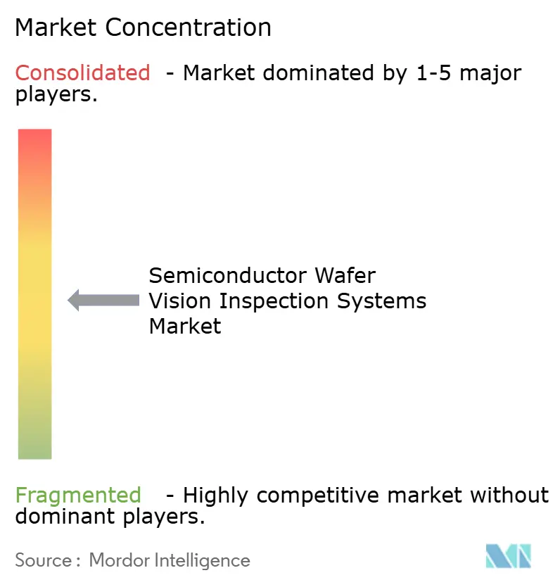
| Market Concentration | Medium |
Major Players *Disclaimer: Major Players sorted in no particular order Image © Mordor Intelligence. Reuse requires attribution under CC BY 4.0. | |
Semiconductor Wafer Vision Inspection Systems Market Analysis by Mordor Intelligence
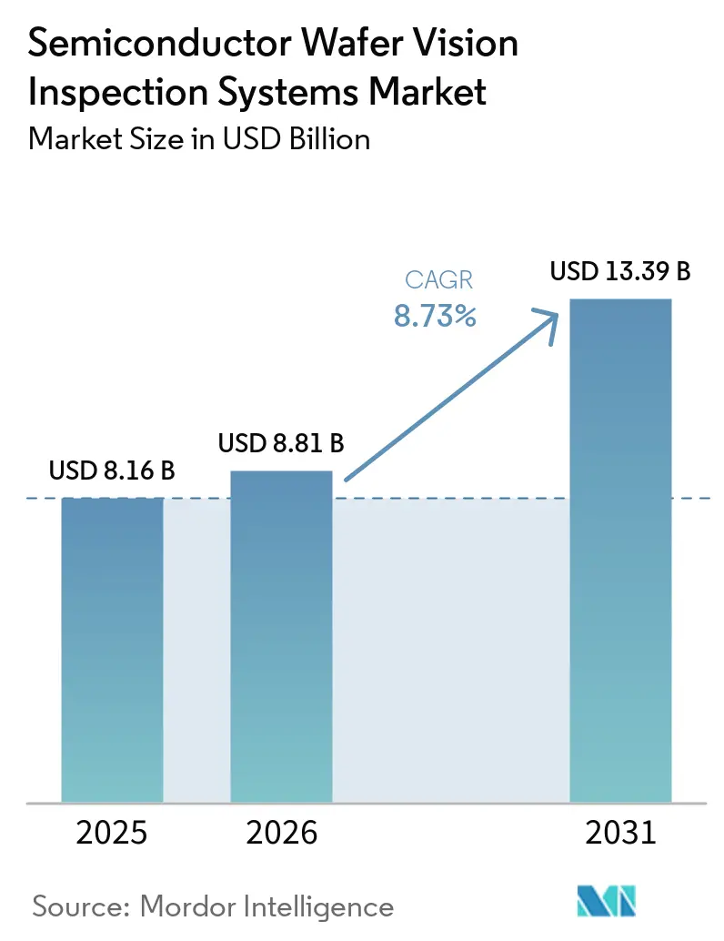
The semiconductor wafer vision inspection systems market size is projected to expand from USD 8.16 billion in 2025 and USD 8.81 billion in 2026 to USD 13.39 billion by 2031, registering a CAGR of 8.73% between 2026 to 2031. Demand is rising because advanced logic, DRAM, and 3D NAND manufacturing require more inspection steps at each process stage, including early checks that prevent a defect from reaching later and more costly layers. Gate-all-around transistors, high-density memory, and taller 3D NAND structures make smaller defects more consequential for wafer yield, so the Semiconductor wafer vision inspection systems market is increasingly tied to process decisions that cannot be delayed until final testing. Artificial intelligence is also moving defect review closer to real-time production control, which raises the value of fast and accurate classification and reduces the practical reliance on manual review of routine defect images. New fabrication plants add demand for complete process-control tool sets, while established fabs need capabilities that can address harder-to-detect defects, creating parallel opportunities for new installations and upgrades. The Semiconductor wafer vision inspection systems market, therefore, favors suppliers that combine imaging performance, software, installed-base support, timely qualification at customer sites, and service teams that can help customers convert inspection results into usable process feedback.
Key Report Takeaways
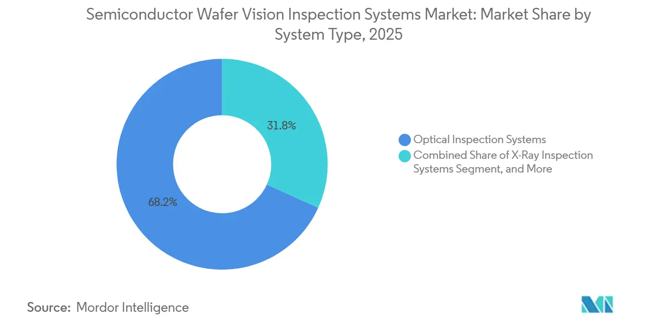
- By system type, optical inspection systems held 68.23% of the semiconductor wafer vision inspection systems market share in 2025, while e-beam Inspection and review systems are projected to expand at a 10.60% CAGR through 2031.
- By wafer surface and pattern, patterned wafer inspection accounted for 73.14% of the market in 2025 and is projected to expand at an 11.30% CAGR through 2031.
- By inspection mode, inline inspection held 65.93% of the semiconductor wafer vision inspection systems market in 2025 and is projected to expand at a 10.50% CAGR through 2031.
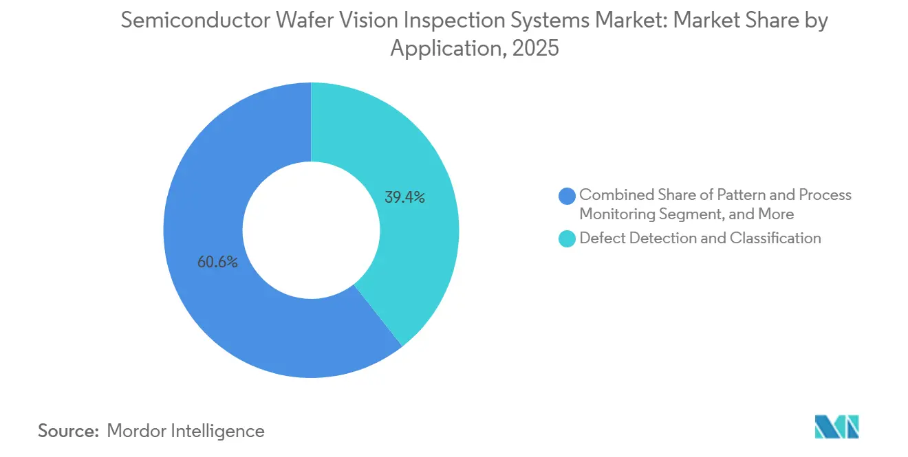
- By application, defect detection and classification accounted for 39.41% of the market in 2025, while critical layer and lithography process inspection is projected to expand at a 10.87% CAGR through 2031.
- By end-user industry, semiconductor foundries held 42.83% of the semiconductor wafer vision inspection systems market in 2025, while memory manufacturers are projected to expand at a 10.15% CAGR through 2031.
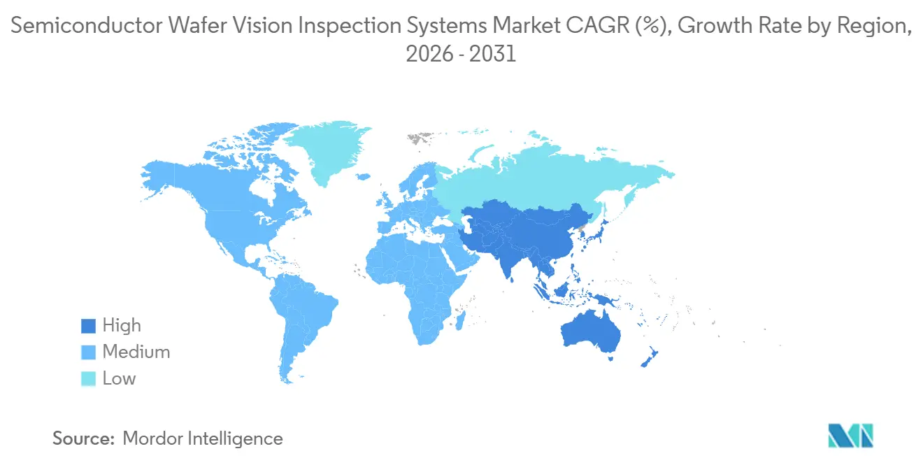
- By geography, Asia-Pacific held 66.11% of the market in 2025 and is projected to expand at an 11.21% CAGR through 2031 in the semiconductor wafer vision inspection systems market.
Note: Market size and forecast figures in this report are generated using Mordor Intelligence’s proprietary estimation framework, updated with the latest available data and insights as of January 2026.
Global Semiconductor Wafer Vision Inspection Systems Market Trends and Insights
Drivers Impact Analysis*
| DRIVER | (~) % IMPACT ON CAGR FORECAST | GEOGRAPHIC RELEVANCE | IMPACT TIMELINE |
|---|---|---|---|
| AI-Enabled Defect Classification and Closed-Loop Yield Control | +1.8% | Global, with greatest intensity in Asia-Pacific foundry and memory clusters | Short term (≤ 2 years) |
| Advanced-Node and 3D Device Complexity | +1.6% | Global, concentrated in Taiwan, South Korea, and U.S. advanced-logic sites | Short term (≤ 2 years) |
| Heterogeneous Integration, HBM, and Chiplet Packaging | +1.4% | Asia-Pacific core, with expansion into North America through CoWoS and advanced packaging | Medium term (2-4 years) |
| Fab Regionalization and Government-Supported Capacity Expansion | +1.2% | North America and Europe, with secondary effects in India, Japan, and the Middle East | Medium term (2-4 years) |
| Automotive and Power Semiconductor Quality Requirements | +0.9% | Europe, North America, and Japan, with growing influence in China and Southeast Asia | Medium term (2-4 years) |
| Compound Semiconductor Adoption for EVs, 5G, and Power Electronics | +0.7% | Global, with early commercial scale in North America, Japan, and Europe | Long term (≥ 4 years) |
| Source: Mordor Intelligence | |||
AI-Enabled Defect Classification and Closed-Loop Yield Control
AI-based classification is linking inspection results more directly with yield-control decisions in high-volume semiconductor production. Onto Innovation reported that its ADC Total Solution reduced nuisance defects from more than 2,000 per inspection run to fewer than 100 in 300mm redistribution-layer production trials. The same work reported 100% wafer-level pattern classification accuracy and a defect escape rate below 0.03%.[1]Bryce Chi, Austin Hsu, Jay Chen, Andy Chen, and Maruko Wu, “Scalable AI-Driven Inspection for Inline Nuisance Filtering and Whole Wafer Pattern Classification,” SPIE Proceedings, spie.org. ASML reported that its Computational Guided Inspection improved defective-die capture by up to 4.3 times at Micron memory manufacturing sites when compared with static sampling plans. These results reduce the manual review burden and allow fabs to respond faster when a process drift appears. The semiconductor wafer vision inspection systems market benefits when inspection platforms can translate large volumes of images into decisions that production teams can use without delay.
Advanced-Node and 3D Device Complexity
New device architectures change the defects that can limit yield, rather than simply requiring finer optical sensitivity. Gate-all-around devices can introduce nanosheet and gate-dielectric defects that are difficult to identify through conventional high-throughput optical methods. Applied Materials introduced its SEMVision H20 system in February 2025 for buried nanoscale defects in 2nm logic, advanced DRAM, and 3D NAND production.[2]Applied Materials, “Applied Materials Accelerates Chip Defect Review with Next-Gen eBeam System,” ASM International Electronic Device Failure Analysis Society, asminternational.org. KLA introduced its 3935 and 3920 EP broadband plasma systems in April 2025 for sensitive logic and memory inspection at 5nm nodes and below. Greater design density also increases the number of inspections needed before defects spread through later wafer-processing steps. The semiconductor wafer vision inspection systems market gains support from this higher inspection intensity, even when a manufacturer does not add new fab capacity.
Heterogeneous Integration, HBM, and Chiplet Packaging
HBM, chiplets, and through-silicon-via structures create inspection needs that differ from those of conventional planar wafers. These designs rely on reliable bonding and alignment across multiple dies, which raises the cost of an undetected defect before final assembly. Onto Innovation launched the Dragonfly G5 platform in March 2026 with 150nm defect sensitivity, machine-learning die-to-die detection, and more than 3 times the predecessor's throughput. A leading HBM manufacturer is committed to double-digit Dragonfly G5 units after its evaluation process. The semiconductor wafer vision inspection systems market is expanding into workflows that require optical, infrared, X-ray, and analytical capabilities to work together. This increases the importance of platforms that can inspect complex structures without slowing production unnecessarily.
Fab Regionalization and Government-Supported Capacity Expansion
Government-backed construction programs are creating demand for process-control equipment at new production sites. The CHIPS for America program allocated USD 39 billion in manufacturing incentives across 40 projects involving 19 companies, and it had committed USD 30.7 billion in awards and USD 5.5 billion in loans by January 2025. TSMC announced an incremental USD 100 billion U.S. manufacturing investment in July 2026, in addition to its existing USD 65 billion commitment. Each greenfield fab requires inspection tools for incoming qualification, inline monitoring, and outgoing quality control. Vendors must also support separate qualification work when production recipes are established in a new geography. This creates longer procurement cycles and rewards semiconductor wafer vision inspection systems market participants with broad service coverage and established customer relationships.
Restraints Impact Analysis*
| RESTRAINT | (~) % IMPACT ON CAGR FORECAST | GEOGRAPHIC RELEVANCE | IMPACT TIMELINE |
|---|---|---|---|
| High Capital and Integration Cost of Advanced Inspection Tools | -1.1% | Global, most acute for legacy 200mm facilities and emerging-market fabs | Short term (≤ 2 years) |
| Export Controls and Fragmented Compliance Requirements | -0.9% | China, Macau, and 21 additional arms-embargo countries under U.S. EAR | Medium term (2-4 years) |
| Shortage of Skilled Inspection and Process-Control Engineers | -0.5% | Global, most acute in new fab locations in North America, Europe, and India | Medium term (2-4 years) |
| Optical and E-Beam Data-Volume and Compute Burden | -0.4% | Global, proportional to advanced-node fab density | Long term (≥ 4 years) |
| Source: Mordor Intelligence | |||
High Capital and Integration Cost of Advanced Inspection Tools
Advanced optical and e-beam platforms are among the most expensive individual equipment purchases within a wafer fab. Costs rise when buyers require high throughput, greater sensitivity, and several inspection capabilities on one platform. The hardware purchase is only part of the commitment because the tool must also connect with process-control software and automated material-handling systems. AI-enabled workflows can add data management and model maintenance requirements for the customer. Smaller manufacturers and 200mm facilities can face a longer return period because their production economics are based on mature nodes. These conditions can slow equipment refreshes in parts of the semiconductor wafer vision inspection systems market that do not operate at the leading edge.
Export Controls and Fragmented Compliance Requirements
U.S. export controls have made sales and support decisions more complex for suppliers of advanced semiconductor manufacturing equipment. The December 2024 FN5 Rule extended licensing requirements to 21 additional arms-embargo countries beyond the People's Republic of China and Macau, with effect from March 2025.[3]Bureau of Industry and Security, “Commerce Strengthens Restrictions on Advanced Computing Semiconductors, Semiconductor Manufacturing Equipment,” U.S. Department of Commerce, bis.gov. Entity List restrictions can impose transaction-specific licensing requirements, including for some products with U.S.-origin components. These obligations may reduce access to restricted customer groups and require continued compliance management. They also encourage domestic equipment development in markets where overseas systems are harder to obtain. The semiconductor wafer vision inspection systems market is therefore becoming more regional in its competitive structure and customer access.
*Our forecasts treat driver/restraint impacts as directional, not additive. The impact forecasts reflect baseline growth, mix effects, and variable interactions.
Segment Analysis
By System Type, Optical Systems Lead While E-Beam Systems Gain Ground
Optical inspection systems held 68.23% of the semiconductor wafer vision inspection systems market share in 2025. Bright-field and dark-field platforms remain widely used because they offer high throughput across patterned and unpatterned wafer workflows. Their established recipe libraries also support repeatable deployment at high-volume foundries and memory fabs, a practical advantage in the semiconductor wafer vision inspection systems market, as customers can build on familiar workflows rather than start each production qualification from scratch. X-Ray Inspection Systems serve a growing need in advanced packaging and through-silicon-via wafer inspection. They provide non-destructive subsurface imaging where visible-light systems have limited reach.
E-beam inspection and review systems are projected to expand at a 10.60% CAGR through 2031. Their main strength is the ability to resolve sub-10nm defects in buried layers that may not be visible through optical inspection. Gate-all-around devices and backside power delivery networks increase the value of voltage-contrast inspection for contacts and dielectric structures. KIOXIA Iwate began evaluating a gallium nitride-based e-beam platform in September 2025, jointly developed by Photoelectron Soul and Nagoya University. The developers reported more than 20 times greater photocathode durability than conventional e-beam sources, addressing a long-standing production throughput constraint.[4]Nagoya University Institute of Materials and Systems for Sustainability, “New Platform for Semiconductor Inspection and Metrology Developed Through Joint Research by Photo Electron Soul and Nagoya University Begins Validation at KIOXIA Iwate,” Nagoya University, imass.nagoya-u.ac.jp. The move from sampled review toward inline use can increase tool demand and service requirements within the semiconductor wafer vision inspection systems market.



By Wafer Surface and Pattern, Patterned Inspection Supports Advanced-Node Yield
Patterned wafer inspection accounted for 73.14% of the semiconductor wafer vision inspection systems market in 2025 and is projected to expand at an 11.30% CAGR through 2031. The category is used after process layers have formed device features on the wafer. Die-to-die and die-to-database comparisons help separate process defects from the intended circuit layout. This is important at advanced logic and memory nodes, where tight pitches make defect identification more difficult. The semiconductor wafer vision inspection systems market size for patterned workflows is driven by the increasing number of critical layers that require inspection before subsequent processing, which adds cost.
ASML validated a 25-beamlet multi-electron-beam system at Micron DRAM and 3D NAND production sites in 2024. The platform identified voltage-contrast defects as its main use case and physical defects as a secondary capability.[5]ASML Holding N.V., “Multi-Electron Beam Inspection Application in Memory Fab,” SPIE Proceedings, spie.org. Unpatterned Wafer Inspection remains essential for incoming substrate qualification, blanket-film monitoring, and material characterization before device fabrication begins. It has particular relevance for silicon carbide and gallium nitride substrates, where early screening can prevent further processing of defective material. Onto Innovation reported that XY-stage photoluminescence scanning maintained center-to-edge sensitivity across 200mm and 300mm silicon carbide wafers. The category can gain further use as compound semiconductor wafer diameters grow.
By Inspection Mode, Inline Systems Take Priority in Production Control
Inline inspection held 65.93% of the semiconductor wafer vision inspection systems market in 2025 and is projected to expand at a 10.50% CAGR through 2031. It enables manufacturers to identify defect excursions while wafers remain within the production flow. Early detection can stop a contamination event before additional process layers make affected wafers more costly to scrap. This matters more as 3D NAND structures add layers and advanced-node wafers carry higher processing value. Inline platforms must combine speed with sufficient sensitivity for each monitored process step.
At-line inspection provides a middle path for work that requires sample transfer and limited setup near the production line. Offline and Laboratory Inspection remains important for failure analysis, process development, and root-cause work where analytical depth matters more than speed. E-beam review and X-ray computed tomography are particularly relevant in these lower-throughput settings. Large image files are a practical consideration because a high-volume inline optical tool can generate terabytes of data during a shift. Within the semiconductor wafer vision inspection systems market, suppliers are responding by moving more AI inference into inspection platforms rather than relying only on centralized computing resources, which can shorten the feedback path between image capture, defect classification, and a production team's response. This supports faster feedback while helping customers manage the infrastructure demands associated with the semiconductor wafer vision inspection systems market.
By Application, Lithography Inspection Gains Importance at Advanced Nodes
Defect detection and classification accounted for 39.41% of the 2025 semiconductor wafer vision inspection systems market revenue. It covers particle detection, pattern defect identification, and AI-supported defect grouping across multiple inspection modes. The wide scope of this application makes it a core part of day-to-day yield management. Pattern and Process Monitoring is the second-largest application because it tracks systematic variation across tool fleets and production lots. Wafer Qualification and Incoming Quality Control provides a separate check on substrates before they enter critical fabrication stages.
Critical layer and lithography process inspection is projected to expand at a 10.87% CAGR through 2031. EUV mask qualification and sub-3nm process layers require tighter control because small printable defects can create systematic yield loss across a wafer lot. Lasertec released the ACTIS A200HiT actinic EUV patterned mask inspection system in October 2025. It delivered 3 times the inspection speed of the ACTIS A150 while retaining sensitivity for printable-defect detection. Macro-defect detection and photomask-related work complement these applications across packaging and substrate production. The link between EUV adoption and critical-layer inspection supports demand in the semiconductor wafer vision inspection systems market as customers shift to new lithography nodes.
By End-User Industry, Memory Manufacturers Increase Inspection Demand
Semiconductor foundries held 42.83% of the 2025 end-user market. Their position reflects advanced-logic capacity in Taiwan, South Korea, and the United States, where inspection intensity is high at 3nm and below. Integrated Device Manufacturers represent the next major customer group because they manage diverse logic, analog, and power device portfolios. OSAT providers are becoming additional buyers as advanced packaging requires inspection methods once associated mainly with front-end wafer fabs. Wafer manufacturers and specialty substrate producers also need qualification tools that can identify material defects before device production.
Memory manufacturers are projected to expand at a 10.15% CAGR through 2031. HBM stacking and growing 3D NAND layer counts add inspection steps for through-silicon-via processing, thin-die handling, and alignment. Samsung was expanding 1c DRAM capacity to more than 200,000 wafers per month by the end of 2026 through conversions and equipment additions. SK Hynix was also expanding 1b DRAM capacity at M15X and converting M14 and M16 facilities for HBM and server DRAM. These programs raise the value of systems that shorten yield learning cycles, which supports the semiconductor wafer vision inspection systems market across memory-focused customers.
Geography Analysis
Asia-Pacific held 66.11% of the semiconductor wafer vision inspection systems market in 2025 and is projected to expand at an 11.21% CAGR through 2031. Taiwan has dense leading-edge foundry capacity at sub-5nm nodes, which supports high inspection intensity per wafer. South Korea combines HBM and advanced DRAM transitions, increasing demand for optical and e-beam platforms. China presents a different environment because international suppliers face export-related restrictions while domestic equipment companies seek to expand their capabilities. Japan holds a distinct position in actinic EUV mask inspection through Lasertec and its ACTIS product family.
North America and Europe are gaining equipment demand from new fab construction and investments in domestic semiconductor supply chains. The U.S. incentive program supports new facilities that require full sets of qualifications and inline process-control equipment. ZEISS SMT announced a 2026 capacity expansion for semiconductor inspection, metrology, and defect-analysis solutions serving advanced-node and advanced-packaging applications.[6]ZEISS Semiconductor Manufacturing Technology, “ZEISS SMT Expands Capacity for Semiconductor Future,” ZEISS, zeiss.com. Europe also has a precision-optics base that supports the wider semiconductor wafer vision inspection systems market. These regions require suppliers to manage local installations, service needs, and separate production qualifications.
The Middle East and Africa and South America represent a smaller share of global wafer inspection demand. Their activity is linked more to specialty semiconductor, assembly, testing, and technology infrastructure than to leading-edge logic fabs. The United Arab Emirates and Saudi Arabia have pursued technology infrastructure and early discussions around domestic testing and packaging capacity. South America remains more closely tied to electronics manufacturing and packaged-component demand, especially in Brazil. These regions remain peripheral to advanced wafer inspection through 2031, but future fab diversification could create longer-term opportunities for the semiconductor wafer vision inspection systems market.

Competitive Landscape
The semiconductor wafer vision inspection systems market is moderately concentrated at the leading edge because advanced-node production requires specialized platforms and long customer qualification cycles. KLA reported USD 6.63 billion in Wafer Inspection revenue during fiscal 2026. Its Semiconductor Process Control segment accounted for 90% of the company's USD 13.58 billion fiscal 2026 revenue. This installed base supports recurring service, applications work, and recipe development with customers. Patent portfolios around optical paths and defect-classification algorithms add barriers for suppliers seeking to enter the highest-performance categories, especially where customers need consistent performance across high-volume operations and demand proof that a new platform can work with established process recipes.
Onto Innovation and Camtek are important alternatives in advanced packaging inspection. Onto Innovation launched Dragonfly G5 in March 2026 and later qualified it for 2.5D AI packaging applications. Camtek signed an agreement in April 2026 to acquire Visual Layer, a visual AI analytics company, to strengthen AI capability in its inspection and metrology offerings. Lasertec retains a strong position in actinic EUV patterned-mask inspection because the required 13.5nm light-source engineering has long development cycles. These moves show that better classification, throughput, and packaging coverage are central areas of competition.
Open opportunities exist in panel-level packaging inspection, compound semiconductor substrate qualification, and software-led inspection analytics. Chinese suppliers are advancing into front-end inspection as regulatory restrictions alter access to international tools. TZTEK reported that its XIXING bright-field defect inspection system entered production-line evaluation at a leading wafer manufacturer in April 2026. Regional competition may grow where domestic suppliers receive more opportunities to qualify at local fabs. Still, leading suppliers maintain advantages in advanced-node performance, global applications support, and established process recipes. The semiconductor wafer vision inspection systems market is likely to remain concentrated where sub-5nm and EUV requirements are most demanding.
Semiconductor Wafer Vision Inspection Systems Industry Leaders
KLA Corporation
Onto Innovation, Inc.
Camtek Ltd.
Lasertec Corporation
Hitachi High-Tech Corporation
- *Disclaimer: Major Players sorted in no particular order

Recent Industry Developments
- June 2026: Coherent Corp. signed a letter of intent to receive up to USD 50 million in CHIPS and Science Act funding from the U.S. Department of Commerce to expand its indium phosphide semiconductor manufacturing facility in Sherman, Texas. The project, which adds wafer fabrication equipment and cleanroom capacity, is expected to create more than 550 direct manufacturing and engineering roles.
- April 2026: Onto Innovation's Dragonfly G5 system completed qualification for 2.5D AI packaging applications, with initial shipments expected in June 2026, extending the platform's addressable market to a serviceable available market of more than USD 500 million across advanced-packaging process generations.
- April 2026: Camtek Ltd. signed a definitive agreement to acquire Visual Layer, a Tel Aviv-based AI company specializing in large-scale visual data analytics. The acquisition is intended to accelerate AI development across Camtek's inspection and metrology products, with near-term improvements in throughput and classification accuracy and longer-term potential for AI-driven analytics recurring revenue.
- March 2026: Onto Innovation launched the Dragonfly G5 inspection and metrology platform, delivering approximately 5 times throughput improvement, 150nm defect sensitivity, and machine-learning die-to-die detection. A leading HBM manufacturer committed to double-digit numbers of Dragonfly G5 units for HBM4 yield support, displacing the previously established tool of record.


Global Semiconductor Wafer Vision Inspection Systems Market Report Scope
The semiconductor wafer vision inspection systems market comprises automated optical and imaging-based inspection equipment used throughout semiconductor fabrication to detect defects, measure critical dimensions, and ensure quality control on silicon wafers at various process stages. These systems employ advanced machine vision, high-resolution cameras, laser scanning, and AI-powered image analysis to identify particles, pattern defects, scratches, and structural anomalies on wafer surfaces in real-time, enabling manufacturers to maintain yield rates, reduce scrap, and comply with increasingly stringent quality standards as device geometries shrink to nanometer-scale nodes.
The semiconductor wafer vision inspection systems market Report is Segmented by System Type (Optical Inspection Systems, E-Beam Inspection and Review Systems, X-Ray Inspection Systems, and Photoluminescence and Other Specialized Imaging Inspection Systems), Wafer Surface and Pattern (Patterned Wafer Inspection, and Unpatterned Wafer Inspection), Inspection Mode (Inline Inspection, At-Line Inspection, and Offline and Laboratory Inspection), Application (Defect Detection and Classification, Pattern and Process Monitoring, Wafer Qualification and Incoming Quality Control, Critical Layer and Lithography Process Inspection, and Other Applications), End-User Industry (Semiconductor Foundries, Integrated Device Manufacturers, Memory Manufacturers, Outsourced Semiconductor Assembly and Test Companies, and Wafer Manufacturers and Specialty Substrate Producers), and Geography (North America, South America, Europe, Asia-Pacific, and Middle East and Africa). The Market Forecasts are Provided in Terms of Value (USD).
| Optical Inspection Systems |
| E-Beam Inspection and Review Systems |
| X-Ray Inspection Systems |
| Photoluminescence and Other Specialized Imaging Inspection Systems |
| Patterned Wafer Inspection |
| Unpatterned Wafer Inspection |
| Inline Inspection |
| At-Line Inspection |
| Offline and Laboratory Inspection |
| Defect Detection and Classification |
| Pattern and Process Monitoring |
| Wafer Qualification and Incoming Quality Control |
| Critical Layer and Lithography Process Inspection |
| Other Applications |
| Semiconductor Foundries |
| Integrated Device Manufacturers |
| Memory Manufacturers |
| Outsourced Semiconductor Assembly and Test Companies |
| Wafer Manufacturers and Specialty Substrate Producers |
| North America | United States | |
| Canada | ||
| Mexico | ||
| South America | Brazil | |
| Argentina | ||
| Rest of South America | ||
| Europe | Germany | |
| United Kingdom | ||
| France | ||
| Italy | ||
| Spain | ||
| Rest of Europe | ||
| Asia-Pacific | China | |
| Japan | ||
| India | ||
| South Korea | ||
| ASEAN | ||
| Rest of Asia-Pacific | ||
| Middle East and Africa | Middle East | Saudi Arabia |
| United Arab Emirates | ||
| Turkey | ||
| Rest of the Middle East | ||
| Africa | South Africa | |
| Nigeria | ||
| Rest of Africa | ||
| By System Type | Optical Inspection Systems | ||
| E-Beam Inspection and Review Systems | |||
| X-Ray Inspection Systems | |||
| Photoluminescence and Other Specialized Imaging Inspection Systems | |||
| By Wafer Surface and Pattern | Patterned Wafer Inspection | ||
| Unpatterned Wafer Inspection | |||
| By Inspection Mode | Inline Inspection | ||
| At-Line Inspection | |||
| Offline and Laboratory Inspection | |||
| By Application | Defect Detection and Classification | ||
| Pattern and Process Monitoring | |||
| Wafer Qualification and Incoming Quality Control | |||
| Critical Layer and Lithography Process Inspection | |||
| Other Applications | |||
| By End-User Industry | Semiconductor Foundries | ||
| Integrated Device Manufacturers | |||
| Memory Manufacturers | |||
| Outsourced Semiconductor Assembly and Test Companies | |||
| Wafer Manufacturers and Specialty Substrate Producers | |||
| By Geography | North America | United States | |
| Canada | |||
| Mexico | |||
| South America | Brazil | ||
| Argentina | |||
| Rest of South America | |||
| Europe | Germany | ||
| United Kingdom | |||
| France | |||
| Italy | |||
| Spain | |||
| Rest of Europe | |||
| Asia-Pacific | China | ||
| Japan | |||
| India | |||
| South Korea | |||
| ASEAN | |||
| Rest of Asia-Pacific | |||
| Middle East and Africa | Middle East | Saudi Arabia | |
| United Arab Emirates | |||
| Turkey | |||
| Rest of the Middle East | |||
| Africa | South Africa | ||
| Nigeria | |||
| Rest of Africa | |||


Key Questions Answered in the Report
What is the semiconductor wafer vision inspection systems market size?
The semiconductor wafer vision inspection systems market size is projected to expand from USD 8.16 billion in 2025 and USD 8.81 billion in 2026 to USD 13.39 billion by 2031, registering a CAGR of 8.73% between 2026 to 2031.
Why are wafer inspection systems becoming more important?
Advanced logic, DRAM, 3D NAND, and HBM add more process steps and make early defect detection more important for yield control.
Which system type leads semiconductor wafer vision inspection demand?
Optical Inspection Systems held 68.23% of the market in 2025 because they support high-throughput patterned and unpatterned wafer workflows.
Which application is expected to grow fastest through 2031?
Critical Layer and Lithography Process Inspection is projected to grow at a 10.87% CAGR through 2031, supported by EUV and advanced-node requirements.
Which region is projected to grow fastest?
Asia-Pacific is projected to expand at an 11.21% CAGR through 2031, supported by foundry and memory manufacturing in Taiwan, South Korea, China, and Japan.
How do export controls affect inspection equipment suppliers?
Licensing requirements can restrict sales in certain geographies and increase compliance needs, while also creating openings for domestic suppliers.
Page last updated on: