Size and Share of Sapphire Crystal Growth Equipment Market for LED Substrates
Market Overview
| Study Period | 2020 - 2031 |
|---|---|
| Market Size (2026) | USD 233.08 Million |
| Market Size (2031) | USD 304.39 Million |
| Growth Rate (2026 - 2031) | 5.48% CAGR |
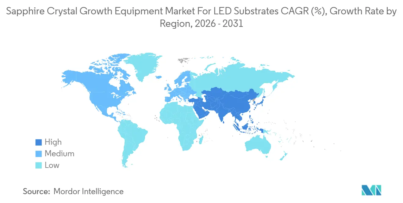
| Fastest Growing Market | Asia Pacific |
| Largest Market | Asia Pacific |
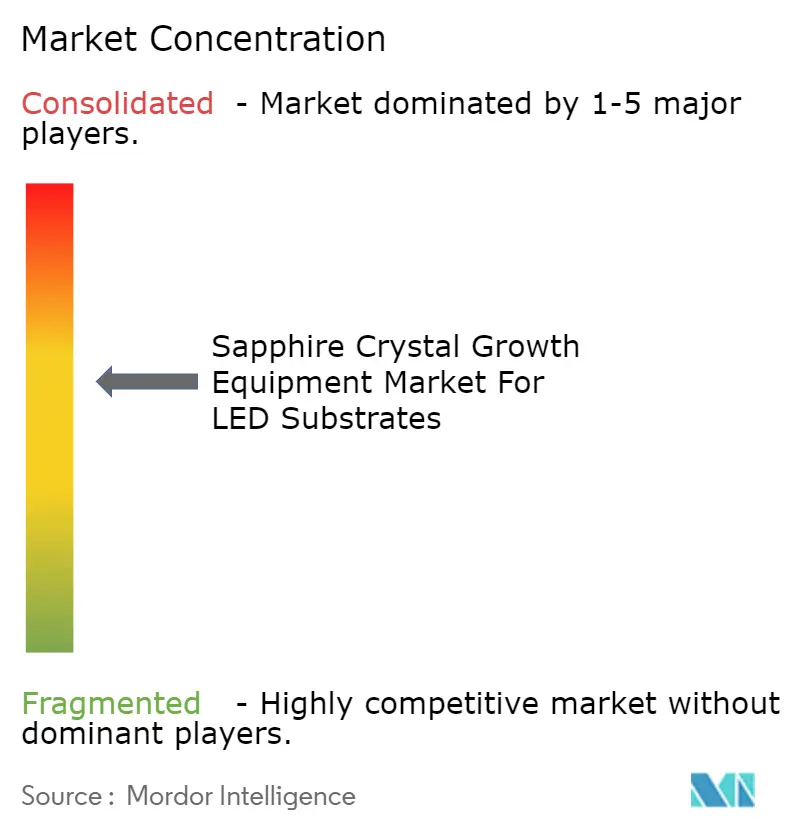
| Market Concentration | Medium |
Major Players *Disclaimer: Major Players sorted in no particular order Image © Mordor Intelligence. Reuse requires attribution under CC BY 4.0. | |
Analysis of Sapphire Crystal Growth Equipment Market for LED Substrates by Mordor Intelligence
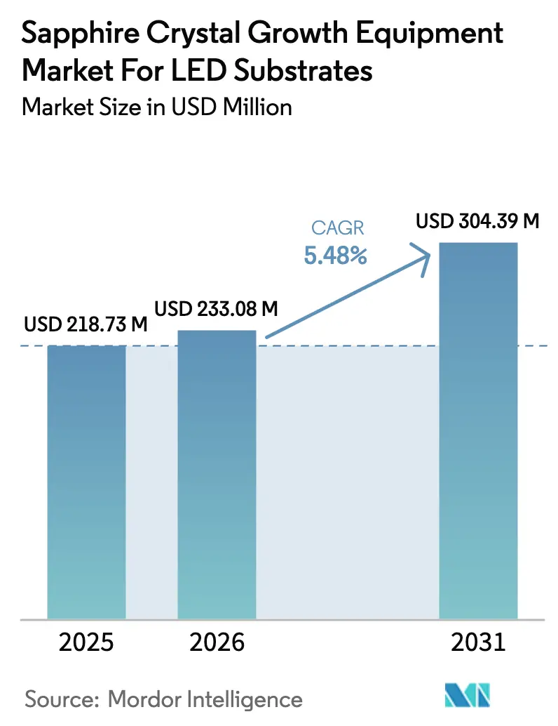
The sapphire crystal growth equipment market for LED substrates market size was valued at USD 218.73 million in 2025, USD 233.08 million in 2026, and reach USD 304.39 million by 2031, at a CAGR of 5.48% during the forecast period (2026-2031). Moderating general-illumination demand in North America and Europe coincides with rising specification pressure from mini-LED backlighting, automotive head-up displays and augmented-reality devices. Chinese epitaxy foundries accounted for roughly 60% of global sapphire wafer capacity additions between 2024 and 2025, yet their recent equipment spend skews toward larger-diameter boules and advanced automation, compressing order cycles for legacy 4-inch lines. Western furnace vendors defend share in above-300 mm systems by leveraging patented thermal-field designs, while Chinese peers gain traction in the 150-300 mm segment through price leadership and localized service. The interplay between premium display uptake and continued LED retrofit mandates under the U.S. Department of Energy and European Union Ecodesign directive will determine whether the projected growth curve accelerates beyond today’s mid-single-digit baseline.
Key Report Takeaways
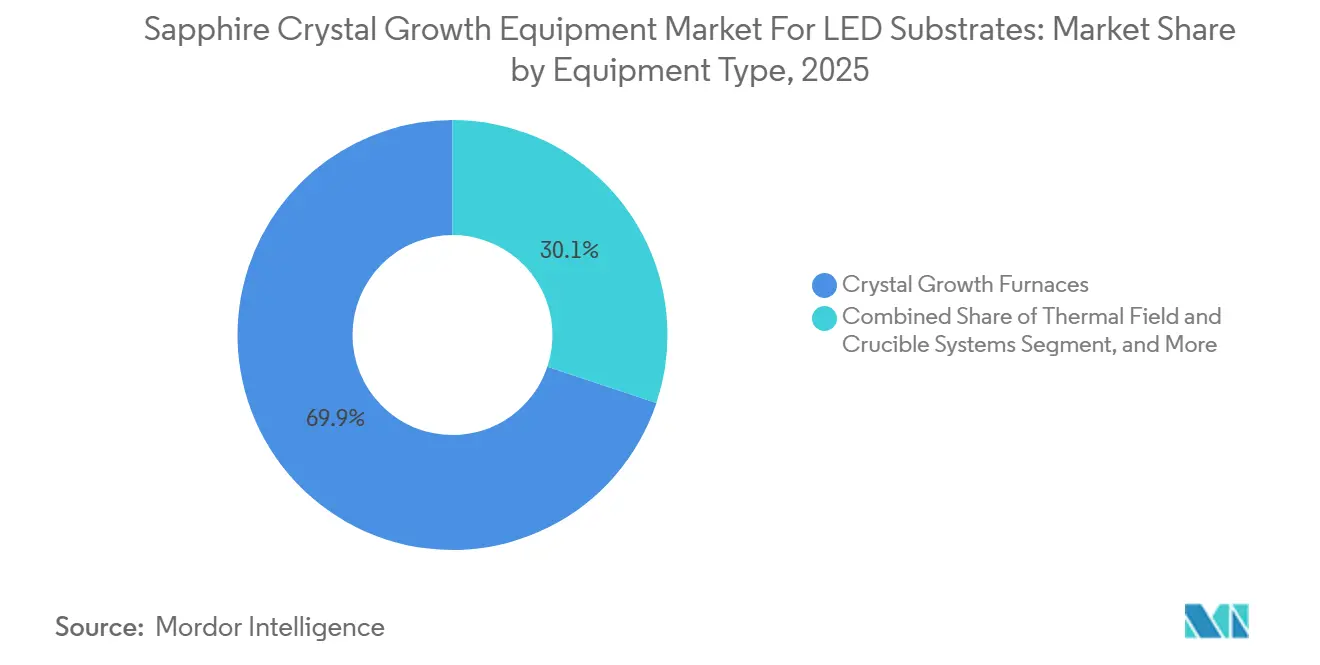
- By equipment type, crystal growth furnaces held 69.87% of the ssapphire crystal growth equipment market for LED substrates market share in 2025, whereas growth automation and process control systems are advancing at a 6.13% CAGR through 2031.
- By growth technology, the Kyropoulos method led with 61.73% revenue share in 2025; Czochralski systems are projected to expand at a 6.59% CAGR to 2031.
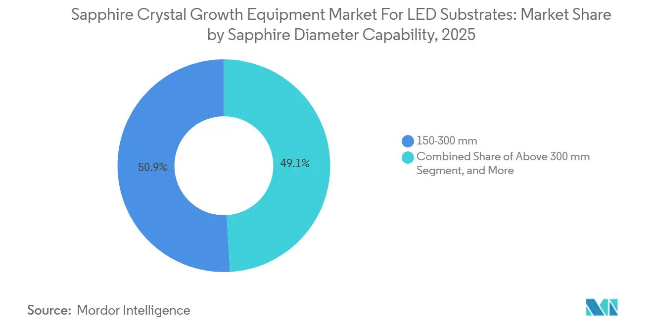
- By diameter capability, 150-300 mm tools accounted for 50.92% of the sapphire crystal growth equipment market for LED substrates market size in 2025, while above-300 mm systems represent the fastest track at a 6.83% CAGR over the same horizon.
- By geography, Asia-Pacific commanded 72.68% revenue share in 2025 and is forecast to grow at a 5.72% CAGR through 2031.
Note: Market size and forecast figures in this report are generated using Mordor Intelligence’s proprietary estimation framework, updated with the latest available data and insights as of January 2026.
Insights and Trends of Sapphire Crystal Growth Equipment Market for LED Substrates
Drivers Impact Analysis*
| Driver | (~) % Impact on CAGR Forecast | Geographic Relevance | Impact Timeline |
|---|---|---|---|
| Aggressive capacity expansion by Chinese epitaxy foundries | +1.4% | Asia-Pacific, particularly China and Taiwan | Short term (≤ 2 years) |
| Surging mini-LED backlighting adoption in high-end TVs | +1.2% | Asia-Pacific core, spillover to North America | Medium term (2-4 years) |
| Transition toward 300 mm sapphire boules to reduce wafer CMP loss | +0.9% | Global, led by Asia-Pacific and North America | Long term (≥ 4 years) |
| Energy-savings mandates from U.S. DOE and EU Ecodesign | +0.7% | North America and Europe, indirect global impact | Medium term (2-4 years) |
| Integration of AI-enabled predictive control in growth furnaces | +0.5% | Global, early adoption in Asia-Pacific | Long term (≥ 4 years) |
| Accelerated capital subsidies for compound-semiconductor clusters in India | +0.3% | India, potential spillover to South Asia | Long term (≥ 4 years) |
| Source: Mordor Intelligence | |||
Aggressive Capacity Expansion by Chinese Epitaxy Foundries
Chinese LED chipmakers commissioned more than 150 new MOCVD reactors during 2024-2025, spearheaded by San’an Optoelectronics and HC SemiTek, whose CNY 2.8 billion (USD 392 million) Yangzhou project targets mini-LED and micro-LED substrates.[1]San’an Optoelectronics, “2024 Annual Report,” sanan-e.com, HC SemiTek, “Yangzhou Expansion Project Announcement,” hcsemitek.com This uptick triggered a near-term spike in demand for 6-inch and 8-inch sapphire wafers, yet it also realigned procurement toward 150-300 mm and above-300 mm furnaces that optimize throughput per boule. State Council funding of CNY 50 billion (USD 7 billion) for compound-semiconductor infrastructure reinforces the build-out, although wafer ASPs slipped 12% year-on-year in Q1 2025, compelling buyers to prioritize automation that compresses cycle time. The net effect raises installed base turnover and lifts attach rates for AI-driven process-control packages, benefiting suppliers able to combine furnace hardware with predictive analytics.
Surging Mini-LED Backlighting Adoption in High-End TVs
Premium television manufacturers shipped roughly 8 million mini-LED sets in 2024, a 35% jump over 2023, with Samsung Electronics and LG Display expanding panel capacity at Paju and other hubs.[2]Samsung Electronics, “2024 Annual Report,” samsung.com, LG Display, “Q2 2025 Earnings Release,” lgdisplay.com Each mini-LED array relies on a higher-quality sapphire substrate to achieve bin-matching for thousands of emissive chips, tightening impurity tolerances to sub-1 ppm. Automotive head-up displays and emerging AR glasses evaluate similar architectures, further lifting demand for defect-free boules. Equipment OEMs now face customer specifications that older Kyropoulos lines can meet only via costly retrofits or complete replacement with Czochralski tools that deliver lower dislocation densities. These premium requirements raise per-furnace ASPs but also lock in higher lifecycle revenue from consumables and software upgrades.
Transition Toward 300 mm Sapphire Boules to Reduce Wafer CMP Loss
Moving from 6-inch to 12-inch boules yields roughly 60% more usable wafer area after slicing and polishing, offsetting the fixed 15-20 µm removal per wafer face. Monocrystal doubled 300 mm output in 2024 to meet Taiwanese and South Korean orders, while PVA TePla reported that above-300 mm furnaces accounted for 28% of its sapphire backlog in mid-2025.[3]Monocrystal LLC, “2024 Annual Results,” monocrystal.com, PVA TePla AG, “Q2 2025 Earnings Call Transcript,” pvatepla.com The migration demands new diamond core-drilling tools and tighter thermal-field uniformity, elevating the value proposition for Western vendors holding IP in large-diameter designs. Although early adopters incur learning-curve yield losses, panel makers aim for wafer costs below USD 5 to unlock wider mini-LED adoption, sustaining momentum toward 300 mm platforms.
Energy Savings Mandates from U.S. DOE and EU Ecodesign
The U.S. DOE’s January 2024 general-service-lamp rule and the EU’s June 2024 Ecodesign revision raised efficacy thresholds that effectively eliminate most legacy lighting technologies.[4]U.S. Department of Energy, “General Service Lamps Final Rule,” energy.gov, European Commission, “Ecodesign Directive Revision for Lighting Products,” europa.eu The International Energy Agency projects an additional 1.2 billion LED lamp installations by 2028. While general-illumination substrates command lower ASPs, they form a durable demand floor that keeps legacy Kyropoulos capacity running at healthy utilization, even as premium display segments pull the technology frontier forward. Compliance pressures also encourage corporate sustainability programs to lock in LED retrofits through 2030, indirectly supporting base-load demand for replacement furnaces.
Restraints Impact Analysis*
| Restraint | (~) % Impact on CAGR Forecast | Geographic Relevance | Impact Timeline |
|---|---|---|---|
| High capex requirement compared with SiC furnace lines | -0.8% | Global, particularly impacting new entrants | Medium term (2-4 years) |
| Volatile alumina prices tightening OEM margins | -0.6% | Global, acute in Asia-Pacific | Short term (≤ 2 years) |
| Yield losses during core-drilling of large-diameter boules | -0.4% | Global, concentrated in early adopters of 300 mm+ tools | Medium term (2-4 years) |
| Sluggish LED lighting retrofit demand in Europe post-2024 | -0.3% | Europe, indirect impact on global supply chains | Short term (≤ 2 years) |
| Source: Mordor Intelligence | |||
High Capex Requirement Compared with SiC Furnace Lines
A turnkey 200 mm sapphire line costs USD 8-12 million, versus USD 5-7 million for an equivalently sized silicon-carbide sublimation setup, while SiC wafers sell at 30-40% higher prices.[5]Wolfspeed Inc., “Fiscal 2025 Earnings Release,” wolfspeed.com Government incentives, notably the U.S. CHIPS Act, disproportionately favor SiC and other wide-bandgap materials, further diverting investment. Payback for sapphire tools stretches to 4-5 years under current LED ASPs, a hurdle for venture-backed entrants seeking quicker returns. Vendors mitigate sticker shock through equipment-as-a-service offerings and outcome-based pricing, yet financing constraints still delay adoption among second-tier fabs.
Volatile Alumina Prices Tightening OEM Margins
Spot prices for 99.99% purity alumina surged 22% between January and April 2025, peaking at USD 4,200 per metric ton before settling near USD 3,800 in June. With raw materials accounting for up to 38% of revenue at major boule producers, sustained volatility squeezes EBITDA and postpones capital upgrades.[6]Monocrystal LLC, “2024 Annual Results,” monocrystal.com Customers increasingly request flexible payment plans or lease-to-own structures, extending sales cycles and challenging vendor working-capital management. Limited hedging instruments leave most of the supply chain exposed to spot-market swings, adding uncertainty to expansion timetables.
*Our forecasts treat driver/restraint impacts as directional, not additive. The impact forecasts reflect baseline growth, mix effects, and variable interactions.
Segment Analysis
By Equipment Type: Automation Outpaces Furnace Upgrades
Crystal growth furnaces anchored 69.87% of 2025 spending, underscoring their central role in the sapphire crystal growth equipment market for LED substrates industry market size. Foundries, however, now increasingly bundle furnaces with software-centric process control packages, lifting automation attach rates to 42% in 2024. The sapphire crystal growth equipment market for LED substrates industry market share for automation and process control systems is poised to expand fastest at 6.13% CAGR through 2031 as wage inflation and tighter display specifications converge. Western OEMs differentiate through AI-driven thermal-field optimization, while Chinese vendors compete on total-cost-of-ownership guarantees that resonate with high-throughput fabs.
Replacement cycles average 8-10 years, yet the pivot to 300 mm compresses depreciation schedules, forcing write-offs of serviceable 6-inch tools. Automation platforms enjoy shorter three-to-five-year refresh intervals, creating a recurring revenue stream that cushions suppliers from furnace order volatility. Consumables such as graphite crucibles and high-purity alumina further lock customers into OEM ecosystems, gradually shifting competitive leverage from hardware price to total solution performance.


By Growth Technology: Kyropoulos Remains Mainstream, Czochralski Gains Precision
The Kyropoulos method captured 61.73% of 2025 revenue thanks to its lower capex and faster cycle times, cementing its role in high-volume general-illumination production. Conversely, the Czochralski approach, favored for mini-LED and micro-LED substrates, is advancing at a 6.59% CAGR, reflecting demand for sub-0.2-degree c-axis misorientation. The sapphire crystal growth equipment market for LED substrates industry market size for Czochralski tools benefits from panel makers willing to pay 20-25% price premiums for superior diameter uniformity. Edge-defined film-fed growth and heat exchanger methods serve niche aerospace and watch-crystal segments, together accounting for under 10% of shipments.
Technology selection also influences downstream costs: Kyropoulos boules display greater radial thermal gradients, complicating automated slicing, whereas Czochralski boules demand longer growth cycles but simplify back-end processing. Equipment vendors thus position hybrid solutions that merge Kyropoulos throughput with Czochralski precision, a strategy evidenced by recent patent filings from PVA TePla and Ferrotec.
By Sapphire Diameter Capability: Mid-Range Dominates, Large-Diameter Momentum Builds
Tools supporting 150-300 mm captured 50.92% revenue in 2025, balancing mature process know-how with economies of scale. Above-300 mm systems, however, present the fastest lane at 6.83% CAGR as panel makers chase wafer-cost deflation. The sapphire crystal growth equipment market for LED substrates industry market share tilt toward 12-inch capability attracts Western vendors holding proprietary thermal-field IP, although Chinese suppliers are rapidly reverse-engineering large-diameter designs to protect domestic share.
Adoption imposes new cost structures: USD 80,000-100,000 diamond core-drills wear out after 200-300 boules, tempering the theoretical yield upside. Nevertheless, early data from Taiwan’s Epistar indicates that 300 mm wafers can deliver sub-USD 5 cost targets even after tooling amortization, reinforcing momentum. Smaller diameter systems persist in R&D labs and specialty optics, but their commercial footprint will continue to erode as mainstream fabs consolidate around 8-inch and 12-inch lines.
Geography Analysis
Asia-Pacific generated 72.68% of the sapphire crystal growth equipment market for LED substrates industry market size in 2025 and is tracking a 5.72% CAGR through 2031. China alone absorbed roughly 55% of global wafer output, fueled by municipal subsidies that offset furnace depreciation. Taiwan specializes in high-margin mini-LED substrates, while South Korea’s Samsung Display and LG Display balloon mini-LED TV capacity, indirectly ratcheting up sapphire substrate pull. Japan’s LED incumbents divert capex to SiC and GaN, yet demand from Nichia and Toyoda Gosei still sustains a niche domestic equipment market.
North America and Europe collectively represented about 18% of 2025 revenue, constrained by limited LED chip fab footprints and subsidy programs skewed toward power electronics. The U.S. CHIPS and Science Act directed only a fractional slice of funding toward sapphire, and Wolfspeed’s strategic pivot to SiC eliminated a major historical buyer. Europe’s Chips Act similarly orients toward advanced logic and SiC, leaving sapphire consumption to specialized vendors such as Monocrystal, whose EU shipments face sanctions-related friction. Regulations still spur LED adoption, but the resulting substrate orders largely accrue to Asian foundries.
The Rest of the World accounted for less than 10% of sales in 2025, yet infrastructure electrification in Saudi Arabia, the UAE and Brazil positions the region for incremental gains. India’s USD 10 billion Semiconductor Mission could alter the map by 2028-2030, though no sapphire tool orders were booked as of March 2026. Equipment OEMs weigh joint-venture assembly models to satisfy potential domestic-content rules, especially as South Asian governments explore localization incentives.
Mordor Intelligence provides coverage of the sapphire crystal growth equipment market for led substrates across other key regional markets, including Asia, each with their regulatory frameworks and demand patterns. Detailed country-level analysis extends to China, Taiwan, and Japan incorporating local coverage and market participation, as required.

Competitive Landscape
The top five vendors, GT Advanced Technologies, PVA TePla, Monocrystal, Cyberstar and Crystal Systems, held an estimated 55-60% share in 2025, underscoring moderate concentration. Western suppliers dominate above-300 mm and Czochralski niches by combining furnace hardware with AI-based process control. Chinese challengers such as Naura Technology Group and Zhejiang Jingjing scale quickly in the 150-300 mm Kyropoulos arena via price undercuts of 20-30% and dense regional service networks.
Strategic focus is shifting toward software differentiation. PVA TePla filed multiple patents for machine-learning heater control, and Ferrotec launched a predictive-maintenance suite promising 20% downtime cuts. Equipment-as-a-service models emerge as financing alternatives, with Toyo Tanso offering lease-to-own crucible packages that translate capex into opex. Hybrid growth furnaces combining Kyropoulos throughput with Czochralski precision form the next innovation frontier, a white-space Western incumbents aim to defend through accelerated R&D spend.
Patent-driven barriers remain significant in thermal-field modeling and crucible metallurgy, yet lower-cost entrants erode pricing power in mainstream diameters. Consolidation pressure persists, but anti-monopoly scrutiny in China and the European Union complicates large-scale mergers, suggesting the industry will stay moderately concentrated rather than converging toward an oligopoly.
Leaders of Sapphire Crystal Growth Equipment Market for LED Substrates
GT Advanced Technologies Inc. (On Semiconductor Corporation)
PVA TePla AG
ECM Greentech S.A. (Cyberstar)
Crystal Systems Inc.
Zhejiang Jingjing Science and Technology Co., Ltd.
- *Disclaimer: Major Players sorted in no particular order

Recent Industry Developments
- February 2026: PVA TePla AG secured a EUR 22 million (USD 23.9 million) contract with a Taiwan-based panel maker for three above-300 mm Czochralski furnaces, incorporating AI thermal-field optimization, with deliveries slated for Q4 2026.
- January 2026: Monocrystal LLC reported USD 180 million sapphire boule revenue for 2025, up 14% year-on-year, after adding two 300 mm Kyropoulos furnaces at its Stavropol plant.
- November 2025: GT Advanced Technologies signed a USD 28 million multiyear supply agreement with a Chinese foundry covering 6-inch and 8-inch furnaces bundled with yield guarantees.
- September 2025: Ferrotec Holdings rolled out an AI-enabled predictive-maintenance platform that reduced unplanned downtime by 20% and raised first-pass yield 12% during pilot deployments.


Scope of Report on Sapphire Crystal Growth Equipment Market for LED Substrates
The Sapphire Crystal Growth Equipment Market for LED Substrates Report is Segmented by Equipment Type (Crystal Growth Furnaces, Thermal Field and Crucible Systems, and Growth Automation and Process Control Systems), Growth Technology (Kyropoulos Method, Edge-Defined Film-Fed Growth, Heat Exchanger Method, and Czochralski Method), Sapphire Diameter Capability (Up to 150 mm, 150-300 mm, and Above 300 mm), and Geography (North America, Europe, Asia-Pacific, and Rest of the World). The Market Forecasts are Provided in Terms of Value (USD).
| Crystal Growth Furnaces |
| Thermal Field and Crucible Systems |
| Growth Automation and Process Control Systems |
| Kyropoulos Method |
| Edge-Defined Film-Fed Growth (EFG) |
| Heat Exchanger Method |
| Czochralski Method |
| Upto 150 mm |
| 150-300 mm |
| Above 300 mm |
| North America |
| Europe |
| Asia-Pacific |
| Rest of the World |
| By Equipment Type | Crystal Growth Furnaces |
| Thermal Field and Crucible Systems | |
| Growth Automation and Process Control Systems | |
| By Growth Technology | Kyropoulos Method |
| Edge-Defined Film-Fed Growth (EFG) | |
| Heat Exchanger Method | |
| Czochralski Method | |
| By Sapphire Diameter Capability | Upto 150 mm |
| 150-300 mm | |
| Above 300 mm | |
| By Geography | North America |
| Europe | |
| Asia-Pacific | |
| Rest of the World |


Key Questions Answered in the Report
How large is the Sapphire Crystal Growth Equipment Market for LED Substrates market today?
It was valued at USD 0.22 billion in 2025 and is forecast to reach USD 0.30 billion by 2031, translating into a 5.48% CAGR.
Which segment shows the quickest growth in this equipment space?
Growth automation and process control systems lead with a projected 6.13% CAGR through 2031 as fabs prioritize AI-driven yield control.
Why are panel makers pushing for 300 mm sapphire wafers?
Moving to 12-inch boules spreads CMP and slicing losses over a larger surface, cutting per-wafer cost and supporting mini-LED display economics.
What restrains wider adoption of sapphire furnaces over SiC?
Sapphire tools cost up to 60% more while SiC wafers capture higher selling prices, lengthening payback periods and dampening new-entrant investment.
Which region dominates equipment demand?
Asia-Pacific holds more than 70% share, driven by Chinese, Taiwanese and South Korean investments in LED and display supply chains.
How are vendors differentiating in a maturing furnace market?
Suppliers increasingly compete on AI-enabled process control, predictive-maintenance software and hybrid growth technologies rather than hardware alone.
Page last updated on:


