
Nano-Magnetic Devices Market Size and Share
Market Overview
| Study Period | 2020 - 2031 |
|---|---|
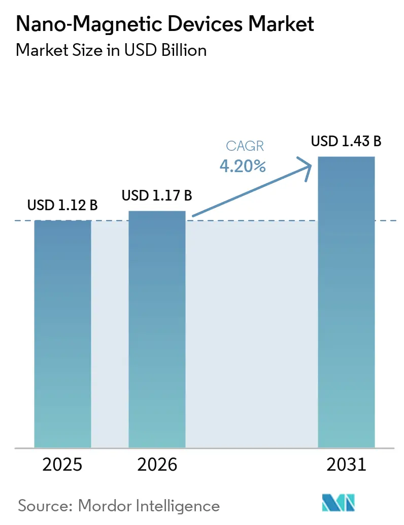
| Market Size (2026) | USD 1.17 Billion |
| Market Size (2031) | USD 1.43 Billion |
| Growth Rate (2026 - 2031) | 4.20 % |
| Fastest Growing Market | Asia Pacific |
| Largest Market | North America |
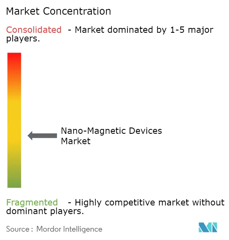
| Market Concentration | Medium |
Major Players
*Disclaimer: Major Players sorted in no particular order Image © Mordor Intelligence. Reuse requires attribution under CC BY 4.0. |
|
Nano-Magnetic Devices Market Analysis by Mordor Intelligence
The nano-magnetic devices market size is expected to grow from USD 1.12 billion in 2025 to USD 1.17 billion in 2026 and is forecast to reach USD 1.43 billion by 2031 at 4.20% CAGR over 2026-2031. Demand escalates as spin-based architectures displace charge-based electronics, offering lower power consumption and faster switching.[1]U.S. Department of Energy, “Draft_EES2_Roadmap_AMMTO,” energy.gov Government incentives from the CHIPS and Science Act and the EU Chips Act accelerate research, while 300 mm fab upgrades lift manufacturing yields for GMR and TMR sensors. Automotive qualification of MRAM for over-the-air updates, deep-space demand for radiation-hardened memory, and Asia-Pacific fab expansion reinforce long-term growth. Nevertheless, export controls on cobalt and gallium, sub-10 nm patterning losses, and areal density limits for next-gen HDDs temper near-term momentum.
Key Report Takeaways
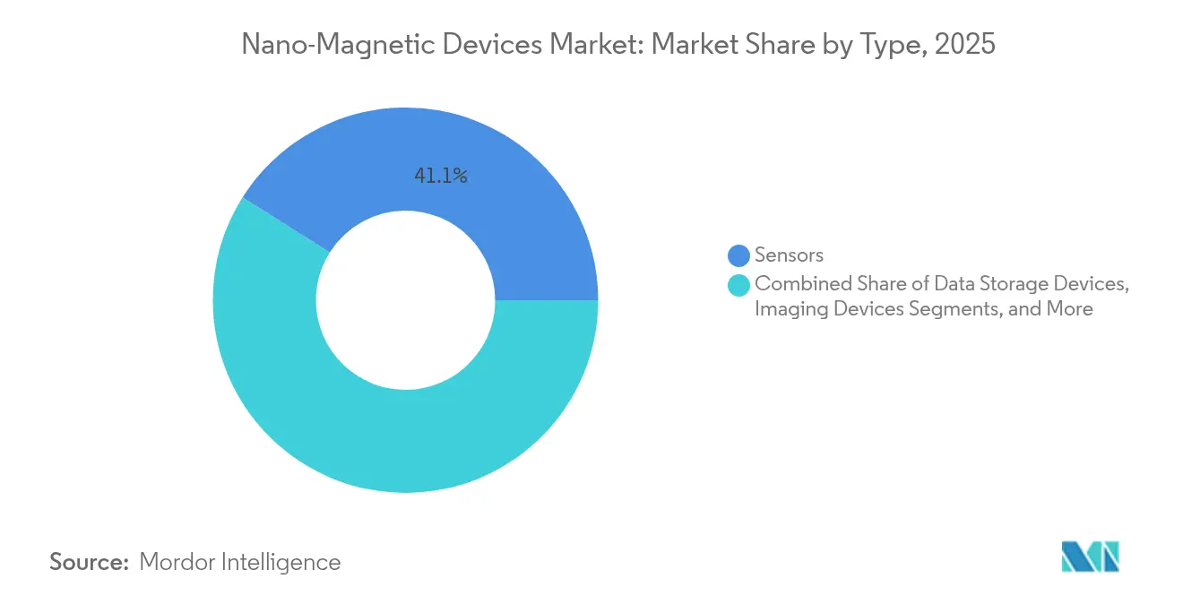
- By type, sensors led with 41.05% revenue share in 2025; data storage devices are projected to expand at a 6.01% CAGR to 2031.
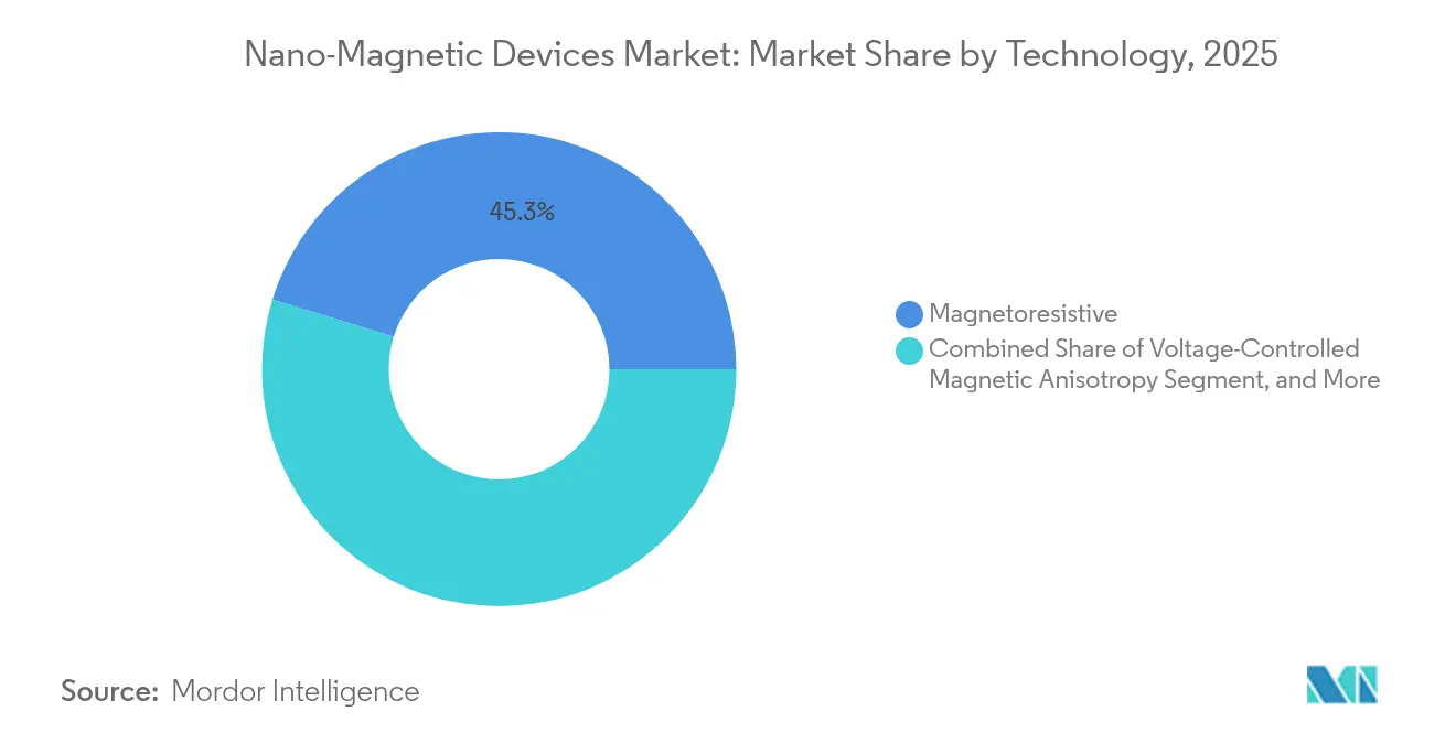
- By technology, magnetoresistive devices held 45.25% of the nano-magnetic devices market share in 2025, while spin-transfer torque technology is advancing at a 5.23% CAGR through 2031.
- By end-use vertical, consumer electronics accounted for 37.44% of the nano-magnetic devices market size in 2025 and automotive & transportation is set to rise at a 5.32% CAGR through 2031.
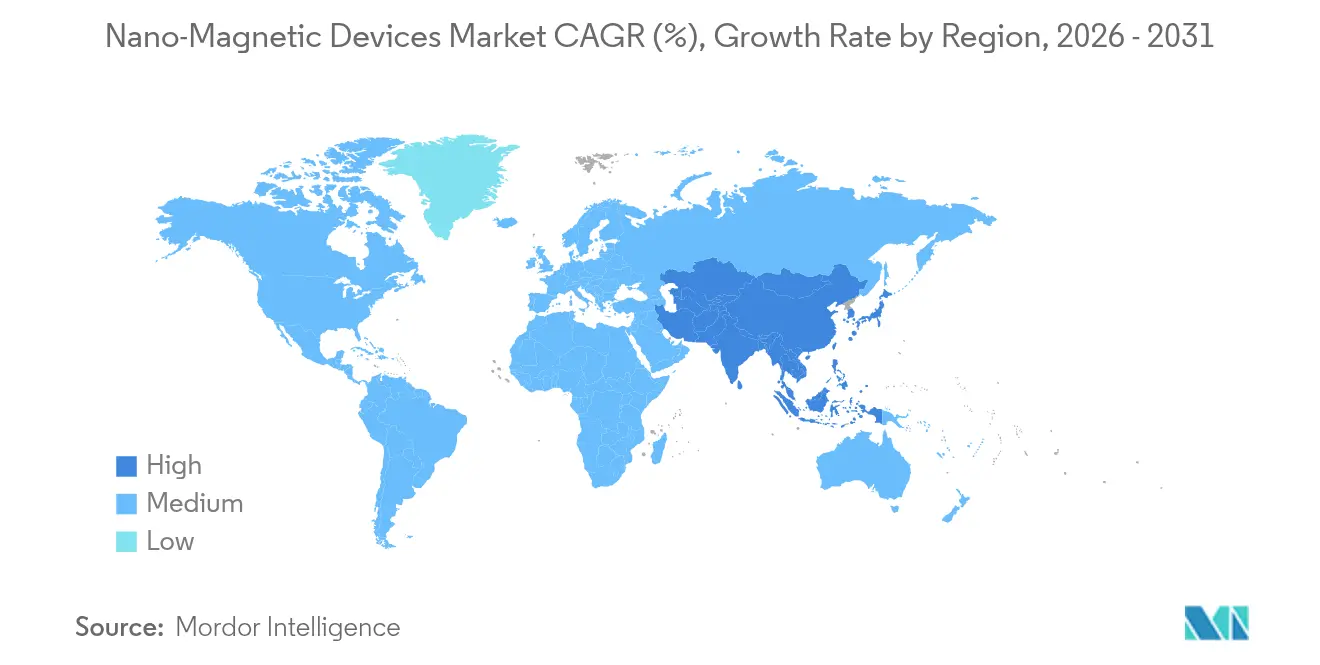
- By geography, North America commanded 31.25% of the nano-magnetic devices market in 2025, whereas Asia-Pacific is the fastest-growing region with a 4.83% CAGR through 2031.
Note: Market size and forecast figures in this report are generated using Mordor Intelligence’s proprietary estimation framework, updated with the latest available data and insights as of 2026.
Global Nano-Magnetic Devices Market Trends and Insights
Drivers Impact Analysis*
| Driver | (~) % Impact on CAGR Forecast | Geographic Relevance | Impact Timeline |
|---|---|---|---|
| Automotive qualification of MRAM for OTA updates | +0.8% | North America & EU | Medium term (2-4 years) |
| 300 mm fab upgrades for GMR/TMR sensors | +0.6% | Asia-Pacific, global supply | Short term (≤2 years) |
| Radiation-hard spintronic memory for deep-space missions | +0.4% | North America & EU | Long term (≥4 years) |
| Shift to NdFeB nano-composite magnets in Chinese wind turbines | +0.5% | Asia-Pacific, global | Medium term (2-4 years) |
| CHIPS & EU Chips Act funding for spintronics | +0.7% | Global | Long term (≥4 years) |
| 3-D LiDAR-magnetic fusion sensors for AMRs | +0.3% | Asia-Pacific, global | Short term (≤2 years) |
| Source: Mordor Intelligence | |||
Automotive Qualification of MRAM for OTA Firmware Updates
Automotive OEMs now certify MRAM that endures unlimited write cycles, eliminating the wear-out concerns of flash memory in software-defined vehicles. TSMC’s embedded MRAM enables microcontrollers that manage frequent over-the-air patches without data corruption.[2]Taiwan Semiconductor Manufacturing Company, “Embedded Non-Volatile Memory for Automotive Applications,” tsmc.com TDK reinforced momentum by unveiling the TAS8240 redundant TMR angle sensor that complies with ASIL D safety norms while operating up to 150 °C. Electric-vehicle production is projected to rise 27%, intensifying demand for magnetic sensing in battery and drivetrain modules.[3]TDK Corporation, “Magnetic sensors: TDK presents new redundant analog TMR angle sensor,” tdk.com Together, robust memory endurance and high-precision sensing cement the nano-magnetic devices market as a core enabler for future automotive electronics.
300 mm Fab Upgrades for GMR/TMR Sensor IC Production
East-Asian foundries have validated 99.6% yield for spin-orbit-torque MTJs on 300 mm wafers, with switching currents of 680 µA at 2 ns and TMR ratios above 119%. These yields drive down unit costs and let manufacturers integrate multi-axis sensors on a single die. Tohoku University guidelines on single-nanometer MTJs secure data retention beyond 10 years at 150 °C while retaining sub-10 ns speed. EUV lithography now reaches 5 nm resolution, guiding further miniaturization. Cost-competitive high-density sensors broaden adoption in consumer electronics and industrial automation, accelerating the nano-magnetic devices market.
Radiation-Hard Spintronic Memory Demand for Deep-Space Missions
Everspin secured USD 9.25 million to supply MRAM macros for radiation-hardened aerospace systems, spotlighting magnetic memory’s resilience under heavy ion exposure.[4]Everspin Technologies, “Contract to Provide MRAM Technology for Radiation Hardened eMRAM,” investor.everspin.com NASA data show MRAM maintains functionality after high-dose gamma and neutron irradiation, a feat unachievable with flash or DRAM. Honeywell’s space-qualified MRAM products target 15-20 year lifespans without wear-out, critical for missions beyond Mars. These capabilities expand the nano-magnetic devices market into deep-space platforms where conventional silicon memories falter.
Shift to NdFeB Nano-Composite Magnets in Chinese Wind Turbines
Chinese turbine makers reduce rare-earth dependency by introducing NdFeB nano-composite magnets that cut particle diameter from 730 nm to 76 nm, raising magnetic energy. Wet ball-milling aided by ethanol enhances uniformity, enabling lighter generators with higher output. Upgraded magnets support rapidly expanding offshore wind installations and create technology spill-overs for global OEMs. The resulting volume demand underpins regional supremacy in the nano-magnetic devices market.
Restraints Impact Analysis*
| Restraint | (~) % Impact on CAGR Forecast | Geographic Relevance | Impact Timeline |
|---|---|---|---|
| Critical mineral export controls on cobalt & gallium | -1.2% | Global, acute in North America & EU | Short term (≤2 years) |
| Sub-10 nm patterning yield losses | -0.8% | Global advanced manufacturing hubs | Medium term (2-4 years) |
| Areal density ceiling <3 Tb/in² for HDDs | -0.4% | Global data storage players | Long term (≥4 years) |
| Lack of IEC/JEDEC TMR-sensor standards | -0.6% | Global regulators | Medium term (2-4 years) |
| Source: Mordor Intelligence | |||
Critical Mineral Export Controls on Cobalt and Gallium
China supplies 98% of global gallium, so potential export bans could shave USD 3.4 billion from U.S. GDP and lift gallium prices more than 150%. Gallium arsenide and gallium nitride devices often co-package with magnetic sensors in RF modules, so shortages reverberate through the nano-magnetic devices market. The Pentagon’s radar modernization that relies on GaN further heightens strategic exposure. Recycling initiatives and AI-guided magnet design aim to mitigate risk, but near-term volatility persists.
Sub-10 nm Patterning Yield Losses in Nano-Magnet Fabrication
Creating high-anisotropy islands below 10 nm incurs stochastic EUV resist failures and line edge roughness that slash wafer yields. IMEC’s High-NA EUV lab will pilot 0.55 NA tools by 2026, yet mass production viability is unproven. Until process windows widen, manufacturers cap investments, restraining the nano-magnetic devices market trajectory.
*Our forecasts treat driver/restraint impacts as directional, not additive. The impact forecasts reflect baseline growth, mix effects, and variable interactions.
Segment Analysis
By Type: Data Storage Drives Innovation Despite Sensor Dominance
Sensors dominated 41.05% of the nano-magnetic devices market in 2025, anchored in automotive, industrial, and mobile products. Data storage devices, however, clock a 6.01% CAGR, propelling the nano-magnetic devices market size for storage from USD 0.24 billion in 2026 to USD 0.33 billion by 2031. MRAM’s non-volatility and radiation tolerance underpin adoption in space probes and electric vehicles. Imaging devices gain traction thanks to ultra-sensitive xMR components that capture biomagnetic signals, creating new revenue pools.
MRAM’s unlimited endurance outperforms flash, removing OTA bottlenecks in passenger vehicles. Breakthrough 3-D magnetic recording promises 10 Tbit/in² capacities, sustaining HDD relevance. Emerging spin-logic integrates memory and compute, foreshadowing in-memory processing paradigms.



By Sensors: TMR Technology Challenges Hall-Effect Dominance
Hall-effect sensors held 41.08% of sensor revenue in 2025 due to low cost and mature supply chains. TMR sensors expand at 5.61% CAGR, narrowing the price gap as 300 mm fabs ramp volume. The TAS8240 redundant angle sensor meets ISO 26262 ASIL D, signaling automotive readiness.
GMR occupies mid-tier niches, balancing sensitivity with affordability. Magnetostrictive sensors excel in aerospace hydraulic controls where EMI immunity is vital. TMR-based digital compasses slash azimuth errors from 4.18° to 0.46° after calibration, improving drone navigation. A new 3-axis silicon Hall sensor with offset cancellation lifts sensitivity to 198 V A⁻¹ T⁻¹, showing the Hall family can still innovate.
By Technology: Spin-Transfer Torque Emerges as Next-Generation Platform
Magnetoresistive approaches commanded 45.25% of the nano-magnetic devices market share in 2025, yet spin-transfer torque devices advance at a 5.23% CAGR through 2031. STT-MRAM achieves 680 µA switching currents at 2 ns while retaining data for 10 years at 150 °C.
Voltage-controlled anisotropy research seeks even lower power writes, and spin-orbit torque promises sub-nanosecond flips with high endurance. Cryogenic growth of ultrathin CoFe on MgO paves the way for single-nanometer MTJs. IEEE’s Beyond-CMOS roadmap lists STT- and SOT-MRAM as key options for memory hierarchy redesign
By End-Use Vertical: Automotive Applications Accelerate Beyond Consumer Electronics
Consumer electronics kept 37.44% revenue share in 2025, powered by smartphones and wearables embedding miniaturized magnetometers. Miniaturized magnetometers in smartphones and wearables support demand in the magnetometer market. Automotive and transportation grow 5.32% annually, lifting the nano-magnetic devices market size for mobility from USD 0.2 billion in 2026 to USD 0.26 billion by 2031 as OTA architectures mature.
Electric-vehicle growth of 27% stimulates TMR demand in battery management and motor control. Medical devices adopt trademarked Nivio xMR sensors that perform magnetocardiography outside shielded rooms, broadening preventive cardiology reach. Aerospace and defense platforms rely on radiation-hard MRAM for mission-critical data logging. Wind energy integrates nano-composite magnets for lighter generators.
Geography Analysis
North America captured 31.25% of the nano-magnetic devices market in 2025, propelled by defense and space programs requiring radiation-tolerant MRAM. Robust university-industry collaborations harness CHIPS Act funding to prototype neuromorphic spintronic chips. The region’s aerospace supply chain values memory endurance over cost, supporting premium pricing.
Asia-Pacific is projected to post a 4.83% CAGR, benefitting from 300 mm fab ramps in Japan, Korea, and China. China’s shift to NdFeB nano-composite magnets strengthens domestic turbine makers and sparks global trickle-down effects. Deployment of 3-D LiDAR-magnetic fusion sensors in Japanese and Korean AMRs underpins smart-factory expansion.
Europe allocates EUR 15.8 billion for Chips Joint Undertaking projects, carving a niche in skyrmionic neuromorphic computing. Germany’s automotive ecosystem demands ASIL D-compliant TMR sensors, while French and Belgian institutes spearhead High-NA EUV lithography. Emerging regions in South America and the Middle East embrace nano-magnetic devices for grid stability and industrial automation, leveraging technology transfer from multinational OEMs.

Regulatory Landscape
Regulation affecting nano-magnetic devices is shaped primarily by end-use compliance, particularly when nanomaterials are embedded in medical and healthcare instrumentation or when occupational exposure occurs during fabrication. In the European Union, the Medical Device Regulation (EU) 2017/745 (MDR) treats medical devices incorporating nanomaterials as high-risk under Rule 19, which is often Class III unless exposure is negligible. This drives higher evidence requirements for safety and performance. EU REACH (EC) No 1907/2006 also imposes nanoform obligations (in place since 2020), influencing materials selection, documentation, and traceability for magnetic stacks and nano-enabled components used across downstream products.
In the United States, nanoscale material oversight is handled through the Environmental Protection Agency framework under TSCA, including Section 8(a) reporting and Significant New Use Rules (SNUR) that can affect specialty magnetic materials and process chemistries. On standards, ISO/TS 12901-1:2024 updates occupational risk-management guidance for manufactured nanomaterials across the lifecycle, reinforcing fab-level EHS controls for MTJ module deposition, etch, and test operations. For medical-device contexts, ISO/TR 10993-22:2017 continues to be a commonly referenced basis for biological evaluation of nanomaterials, shaping qualification pathways for nano-magnetic imaging and sensing components that interface with patients or clinical environments.
Value Chain Analysis
The nano-magnetic devices value chain starts with critical materials and thin-film stacks used to build magnetic tunnel junctions (MTJs), then moves through specialized, equipment-intensive deposition (notably PVD), lithography and patterning, etch, metrology, and reliability screening before integration into CMOS flows. A key midstream step is MTJ module integration into standard semiconductor process lines for products such as MRAM and TMR/GMR sensors, where contamination control and yield management remain recurring bottlenecks. Downstream, device makers distribute qualified components into end-use systems spanning automotive electronics, industrial automation, aerospace and defense, and healthcare instrumentation, with requirements that diverge sharply by vertical (for example, functional safety in automotive versus radiation tolerance and secure packaging in defense programs).
Manufacturing models vary between vertically integrated specialists and hybrid foundry-led strategies. NVE Corporation keeps deposition, patterning, etching, and test in-house at its Minnesota operations while using external foundries for conventional CMOS wafer portions, which helps it maintain tighter control over critical spintronic steps. Everspin uses a hybrid approach, running back-end processing on purchased CMOS wafers at its Chandler, Arizona site and relying on foundry relationships for full-flow production. In April 2026, it deepened on-shore supply by signing a 10-year Foundry Services Agreement with Microchip Technology to manufacture MRAM, TMR sensors, and STT-MRAM wafers at Microchip's Fab 4 in Gresham, Oregon. These partnerships underline that access to qualified fabs and stable MTJ-capable process modules is increasingly central to capacity, quality, and delivery assurance.
Competitive Landscape
The nano-magnetic devices market shows moderate concentration, with integrated device manufacturers and specialized spintronics firms sharing value pools. TDK offers a full magnetic sensor line-up and commands design-win leverage across automotive, industrial, and medical sectors. Everspin cooperates with Frontgrade to meet U.S. defense radiation standards, blending fab capacity with secure packaging investor.
Infineon reorganized in January 2025, forming the SURF unit to co-optimize sensor and RF research for a USD 20 billion opportunity by 2027. IBM advances racetrack memory, forecasting 100-fold capacity gains with ten-million-fold speed improvements, supported by public-private grants. Materials Nexus used AI to design rare-earth-free magnets in three months, indicating computational materials discovery could shorten the innovation cycle.
Automotive Tier-1 suppliers demand ASIL D compliance, pressuring vendors to validate long-term reliability. Consumer electronics favor cost and size, sparking intense price competition among Hall-effect providers. Aerospace clients pay premiums for rad-hard certification, isolating that niche from commodity pressures. Such segmentation shapes strategic alliances, technology roadmaps, and capital allocation across the nano-magnetic devices market.
Nano-Magnetic Devices Industry Leaders
-
IBM Corporation
-
Fujitsu Limited
-
Nanomagnetics Instruments
-
Hitachi Metals America Limited
-
Honeywell International Inc.
- *Disclaimer: Major Players sorted in no particular order

Market Opportunities and Future Outlook
Opportunities concentrate where nano-magnetic devices deliver system-level value under tight power, endurance, reliability, or safety constraints, and where integration hurdles are being addressed through manufacturable architectures. In memory, MRAM production at advanced nodes (noted at 22 nm with development moving toward 16 nm) supports design-in for embedded non-volatile use cases in automotive electronics and other always-on edge systems. Supply-chain moves such as Everspin's April 2026 long-term foundry agreement with Microchip (Fab 4, Oregon) also point to active investment in domestic wafer capacity and multi-product manufacturing for MRAM and TMR sensors. This supports whitespace for device vendors and foundries that can standardize MTJ integration and provide automotive and aerospace-grade qualification data at scale.
Beyond memory, spintronic sensing and security primitives create additional adoption lanes as field-free switching and bias-field elimination become more practical through engineering progress. In June 2026, Huazhong University of Science and Technology and Hubei University demonstrated a spintronic hardware-security architecture using SOT-based Hall devices for physical unclonable functions and true random number generation, aligning nano-magnetic device physics with security-by-design requirements in connected systems. In June 2026, Stanford University advanced a two-terminal field-free architecture for SOT-MRAM and filed patent claims, highlighting an emerging IP-centered route to commercialization around field-free operation, BEOL compatibility, and lower write currents. Together, these proof points indicate near-term whitespace in edge security modules, radiation-tolerant compute nodes, and research-to-pilot transitions where device makers, tool suppliers, and foundries can package manufacturable SOT/STT platforms with qualification collateral rather than standalone lab demonstrations.
Recent Industry Developments
- June 2026: Quantum Design International completed the acquisition of Qnami, adding diamond nitrogen-vacancy (NV) center sensing capabilities for nanoscale magnetic imaging and characterization. The deal broadens Quantum Design's toolchain footprint in nanomagnetism and spintronics R&D, strengthening its ability to support advanced materials and device-development workflows that feed commercial nano-magnetic sensors and memory.
- April 2026: Everspin Technologies and Microchip Technology signed a 10-year Foundry Services Agreement to manufacture MRAM, TMR sensors, and STT-MRAM wafers at Microchip's Fab 4 in Gresham, Oregon. The arrangement reinforces on-shore production options and long-horizon capacity planning for MTJ-based devices, supporting supply assurance for defense, industrial, and automotive programs.
- February 2025: The Chips Joint Undertaking launched EUR 1.67 billion pilot-line calls aimed at sub-2 nm and heterogeneous integration. This program supports process-development infrastructure that can accelerate integration of novel modules such as magnetic stacks into advanced semiconductor flows, helping move spintronic device concepts from research to manufacturable pilot lines.


Research Methodology Framework and Report Scope
Market Definition and Coverage
For this study, the nano-magnetic devices market covers revenue generated from devices and device-level components that use nanoscale magnetic effects to sense, store, image, actuate, or perform logic functions, and that are sold into end-use industries as finished units or integrated modules.
Scope exclusions: We exclude basic bulk magnets and non-device nanomaterials that are sold only as raw powders without a defined device function.
Segmentation Overview
-
By Type
-
Sensors
- Magnetic Field Sensors
- Hall-Effect Sensors
- GMR Sensors
- TMR Sensors
- Magnetostrictive Sensors
-
Data Storage Devices
- MRAM
- Spintronic HDD Read Heads
- Tape Storage Heads
-
Imaging Devices
- Magnetic Particle Imaging Systems
- Nano-MRI Coils
-
Actuators and Logic Devices
- Spintronic Logic/Transistors
- Micromotors and Actuators
-
Other Nano-Magnetic Components
- Antenna and RF Devices
-
Sensors
-
By Technology
- Magnetoresistive
- Spin-Transfer Torque (STT)
- Voltage-Controlled Magnetic Anisotropy (VCMA)
- Superparamagnetic Nanoparticles
-
By End-use Vertical
- Consumer Electronics
- IT and Telecom (Data Centers)
- Automotive and Transportation
- Aerospace and Defense
- Healthcare and Medical Devices
- Energy and Utilities (Wind, Power Converters)
- Industrial Automation and Robotics
- Others (Research and Education)
-
By Geography
-
North America
- United States
- Canada
- Mexico
-
Europe
- Germany
- United Kingdom
- France
- Nordics
- Rest of Europe
-
South America
- Brazil
- Rest of South America
-
Asia-Pacific
- China
- Japan
- India
- South-East Asia
- Rest of Asia-Pacific
-
Middle East and Africa
-
Middle East
- Gulf Cooperation Council Countries
- Turkey
- Rest of Middle East
-
Africa
- South Africa
- Rest of Africa
-
Middle East
-
North America
Data Sources, Market Sizing, and Validation
Desk Research
Desk research starts with public technical and trade data that helps us understand where demand shows up and how quickly it can move. We referred to sources such as the National Institute of Standards and Technology (NIST), the US Patent and Trademark Office (USPTO) database, the International Electrotechnical Commission (IEC), the IEEE Xplore digital library, and the World Semiconductor Trade Statistics (WSTS) updates to frame adoption signals around memory, sensors, and advanced electronics.
After that, we tightened sizing inputs using annual reports, investor decks, product briefs, and credible industry news for manufacturing roadmaps and use case momentum. Where needed, we also used paid subscriptions for company financial intelligence, patent analytics, and news and financial screening to cross-check timelines and directional shifts. The desk sources listed here are illustrative, and we used other public and paid references for data collection, validation, and clarification.
Primary Interviews and Surveys
Primary work focused on validating what portion of nano-magnetic device demand is real in commercial shipments, and what is still mainly pilot scale. We spoke with a balanced mix of device makers, component specialists, integrators, research labs, and downstream users in electronics, data storage, healthcare, and automotive across major regions, so gaps from desk research could be closed with practical inputs.
Distribution of primary research fieldwork respondents
| Company type | Respondent position | Region |
|---|---|---|
| Top tier: 34% | CXOs: 16% | APAC: 44% |
| Mid tier: 46% | Functional/Unit leaders: 40% | EMEA: 32% |
| Smaller Players: 20% | Managers: 44% | Americas: 24% |
Market-Sizing & Forecasting
For market sizing, we used a top down build that starts from electronics and device demand pools, then narrows the addressable share based on adoption of nano-magnetic architectures in real products. We checked the totals through selective bottom-up views, such as sampled shipments by device type and a price range check (ASP times volume) for key applications, and then adjusted when the two views did not align.
Inputs used in the model include indicators such as MRAM and spintronic memory adoption, magneto-resistive sensor penetration in automotive and industrial use, data center storage upgrade cycles, R and D intensity reflected in patent filings, and semiconductor capacity expansion plans tied to advanced nodes. Since pricing can move quickly as designs mature, ASP progression was treated separately by device family, and gaps in public volume data were handled with interview-led ranges and conservative midpoint assumptions.
Forecasts were built using scenario analysis, where base, optimistic, and constrained cases were shaped by expert expectations on commercialization timing, component availability, and qualification cycles in regulated end uses. The final forecast follows the case that best matches observed shipment momentum and near-term design-win pipelines.
Data Validation & Update Cycle
Validation is done in steps so the model does not depend on one data series. Outputs are compared against independent signals such as patent momentum, known ramp schedules in electronics manufacturing, and application-level adoption cues from end users, and then large variances are reviewed before sign-off.
If an assumption shifts sharply, for example a change in storage technology timing or a major supply constraint, we re-contact the relevant interviewees and rerun the affected parts of the model. Reports are refreshed annually, with interim updates when material events occur, and a final pre-delivery review is completed so clients receive the latest updated view.
Mordor Intelligence's Nano Magnetic Devices Market Sizing Compared With Other Published Estimates
Published market sizes for nano-magnetic devices can vary because the boundary between device revenue and adjacent materials or semiconductor content is not always treated the same. Differences also show up when studies mix pilot-stage research activity into commercial demand, or when they assume very fast price declines without checking what buyers are actually paying.
By tracking shipment-linked adoption signals and refreshing scope rules each cycle, Mordor Intelligence keeps the count focused on device-level revenue for sensors, storage, imaging, and logic, which reduces inflation from broad nanomaterials value or full semiconductor wafer value being included.
Benchmark comparison
| Source | Market Size | Gaps in Research Methodology |
|---|---|---|
| Mordor Intelligence | USD 1.17 B (2026) | |
| Global Consultancy A | USD 11.53 B (2025) | The estimate appears to include a much wider value chain, likely counting broader nano-enabled electronics or adjacent nanomaterials spend, which lifts the total beyond device revenue alone. |
| Trade Publisher B | USD 1.16 B (2026) | This number is close on the base year, but scope tends to be simplified by type and application, with limited visibility on pricing logic and how pilot shipments are filtered out. |
The spread is mainly explained by what is counted as in-scope revenue and how early-stage activity is treated. A device-focused boundary, plus repeatable checks against adoption and pricing signals, helps keep the market size traceable to clear demand drivers and easier to update year over year.


Key Questions Answered in the Report
What is the current size of the nano-magnetic devices market?
The nano-magnetic devices market stood at USD 1.17 billion in 2026 and is projected to reach USD 1.43 billion by 2031.
Which segment is growing fastest within the nano-magnetic devices market?
Data storage devices, driven by MRAM adoption, are expected to expand at a 6.01% CAGR through 2031.
Why are TMR sensors gaining traction over Hall-effect sensors?
TMR sensors deliver higher magnetoresistance and better signal-to-noise ratios, enabling compliance with stringent automotive safety standards.
How do export controls on gallium impact the nano-magnetic devices industry?
Potential gallium restrictions could inflate prices by more than 150%, affecting RF modules that integrate magnetic sensors and thus dampening short-term market growth.
Which region will grow the fastest in nano-magnetic devices adoption?
Asia-Pacific is forecast to post a 4.83% CAGR through 2031 owing to large-scale 300 mm fab expansions and wind-energy magnet upgrades.
How does MRAM benefit deep-space missions compared with flash memory?
MRAM offers radiation tolerance and unlimited endurance, ensuring reliable data retention over decades-long deep-space missions
Page last updated on:


 Your data is secure and never sold or shared.


