
Inline Optical Metrology Systems Market Size and Share
Market Overview
| Study Period | 2020 - 2031 |
|---|---|
| Market Size (2026) | USD 4.44 Billion |
| Market Size (2031) | USD 6.72 Billion |
| Growth Rate (2026 - 2031) | 8.64 % |
| Fastest Growing Market | Asia-Pacific |
| Largest Market | Asia-Pacific |
| Market Concentration | High |
Major Players *Disclaimer: Major Players sorted in no particular order Image © Mordor Intelligence. Reuse requires attribution under CC BY 4.0. | |
Inline Optical Metrology Systems Market Analysis by Mordor Intelligence
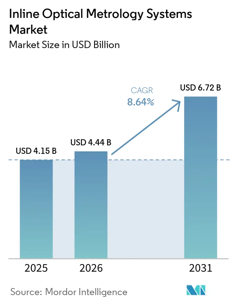
The Inline Optical Metrology Systems Market size was valued at USD 4.15 billion in 2025 and estimated to expand to USD 6.72 billion by 2031, at a CAGR of 8.64% during the forecast period 2026-2031. The Inline Optical Metrology Systems Market is shifting toward measurements taken directly within production lines because smaller device geometries and tighter battery tolerances leave less room for sampling errors. Semiconductor fabrication and advanced packaging remain the primary drivers of demand, while battery production creates a second source of equipment demand. Vendors are pairing optical hardware with analytics, recipe development, fleet management, calibration support, and process-control software to develop recurring revenue and meet tighter factory quality requirements. High tool prices still limit broad deployment outside leading fabs, but they also leave room for lower-cost systems aimed at mid-sized manufacturers. Geographic demand is becoming more distributed as manufacturers add North American capacity while Asia-Pacific remains the largest production base.
Key Report Takeaways
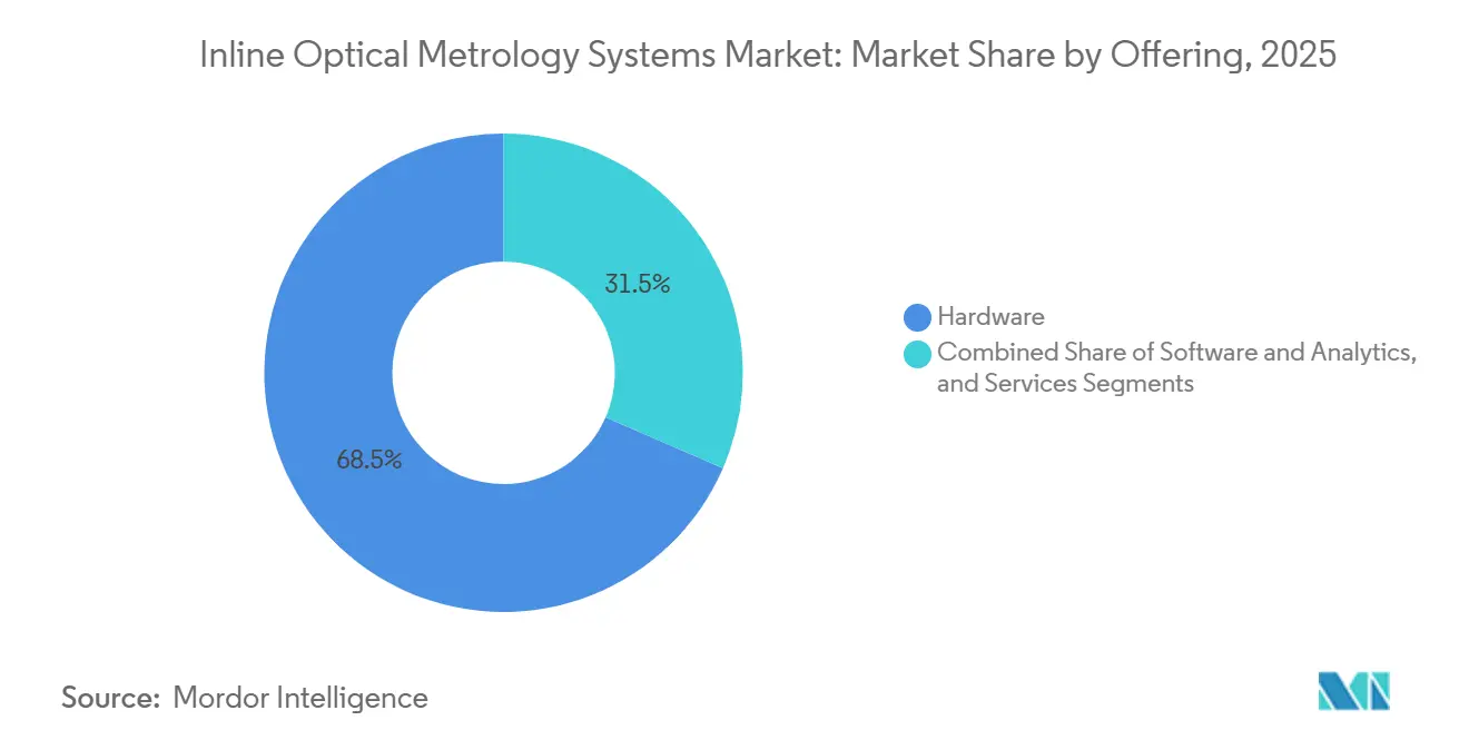
- By offering, hardware held 68.47% Inline Optical Metrology Systems Market revenue share in 2025, while software and analytics are expected to expand at an 11.27% CAGR through 2031.
- By product type, optical critical dimension and scatterometry systems held 24.73% revenue share in 2025, while chromatic confocal and laser triangulation systems are projected to expand at a 10.93% CAGR through 2031.
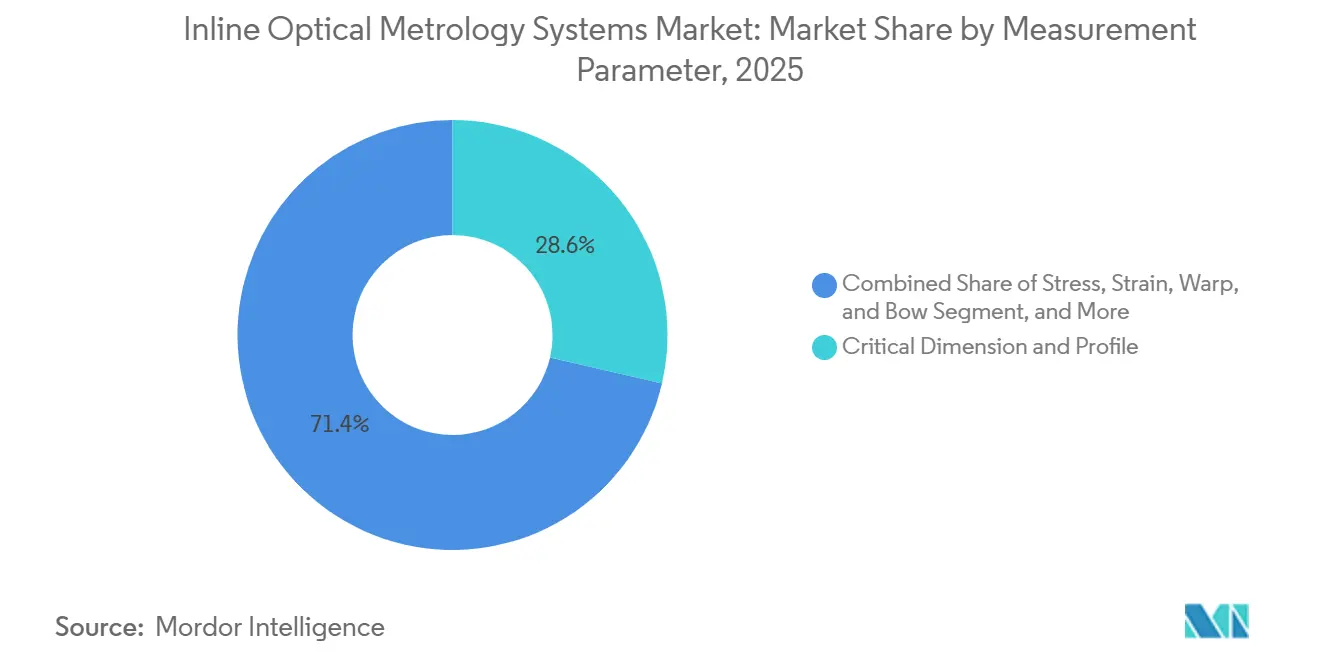
- By measurement parameter, critical dimension and profile held 28.63% Inline Optical Metrology Systems Market revenue share in 2025, while stress, strain, warp, and bow are expected to expand at an 11.47% CAGR through 2031.
- By end-user industry, semiconductors and advanced packaging accounted for 47.83% of revenue in 2025, while battery cells, modules, and packs are projected to expand at an 11.83% CAGR through 2031.
- By geography, Asia-Pacific held 54.67% of the Inline Optical Metrology Systems Market share in 2025 and is projected to expand at a 10.97% CAGR through 2031.
Note: Market size and forecast figures in this report are generated using Mordor Intelligence’s proprietary estimation framework, updated with the latest available data and insights as of January 2026.
Global Inline Optical Metrology Systems Market Trends and Insights
Drivers Impact Analysis*
| Driver | (~) % Impact on CAGR Forecast | Geographic Relevance | Impact Timeline |
|---|---|---|---|
| Zero-Defect and Right-First-Time Manufacturing | +2.4% | Global | Short term (≤ 2 years) |
| Semiconductor, Advanced Packaging, and Compound Semiconductor Capacity Expansion | +2.1% | Asia-Pacific core, spillover to North America and Europe | Medium term (2-4 years) |
| EV Battery and Power-Electronics Production Scaling | +1.5% | Asia-Pacific core, North America, and Europe | Medium term (2-4 years) |
| AI-Enabled Closed-Loop Process Control | +1.2% | Global | Short term (≤ 2 years) |
| Recipe Portability Across Multi-Node and Multi-Plant Production | +0.6% | Global | Medium term (2-4 years) |
| Optical Fingerprinting of Buried Interfaces and Non-Visual Defects | +0.4% | North America and Asia-Pacific | Long term (≥ 4 years) |
| Source: Mordor Intelligence | |||
Zero-Defect and Right-First-Time Manufacturing Requires Real-Time Feedback
Yield pressure at advanced nodes makes immediate feedback increasingly important to the Inline Optical Metrology Systems Market. At process generations below 3 nm, an uncontrolled measurement deviation can spread through a wafer lot and create costly scrap. This changes inline optical metrology from a sampling tool into a requirement for wider wafer coverage and faster corrective action. Fractilia reported in 2025 that its FAME 300 system was integrated into a leading semiconductor manufacturer’s fab automation flow across more than 200 metrology steps. The example shows how fabs are connecting measurement results to production controls rather than using them only for later review. Suppliers that provide stable measurements at production speed are better positioned in advanced manufacturing programs where process windows narrow, production volume increases, and more process steps depend on coordinated inspection and automated corrective decisions
Semiconductor, Advanced Packaging, and Compound Semiconductor Capacity Supports Tool Demand
New fabrication capacity supports the Inline Optical Metrology Systems Market because each advanced production line requires process-control equipment. TSMC announced USD 165 billion in planned manufacturing investment in the United States during March 2025.[1]TSMC, “TSMC Intends to Expand Its Investment in the United States by an Additional USD 100 Billion,” TSMC, tsmc.com The Semiconductor Equipment and Materials International forecast identified 18 new fabrication facilities scheduled to begin construction in 2025, with most expected to start production during 2026 or 2027. The Inline Optical Metrology Systems Market also benefits from compound semiconductor lines, as silicon carbide and gallium nitride substrates have defect requirements that differ from those of silicon. Infinitesima stated in 2025 that its Metron3D 300 mm system provided sub-nanometer 3D process control for DRAM production. Therefore, capacity growth supports conventional optical tools and equipment for three-dimensional structures.
EV Battery and Power-Electronics Production Scaling Creates a New Demand Base
Battery factories are creating a separate equipment opportunity for the Inline Optical Metrology Systems Market. Coating, calendering, slitting, and cell assembly can introduce changes in thickness, density, and edge geometry that affect battery performance and safety. Micro-Epsilon reported that its thicknessCONTROL system completed 12 months of continuous operation at the UK Battery Industrialization Center while maintaining its calibration performance.[2]Micro-Epsilon, “UKBIC Validates Micro-Epsilon Inline Battery Foil Thickness Technology After 12 Months of Successful Operation,” Micro-Epsilon, micro-epsilon.co.uk This measurement can replace offline sampling with continuous production-line verification. A 2026 study reported 7.8 nm precision for terahertz measurement of lithium-ion battery electrode thickness. As battery lines add automation, the Inline Optical Metrology Systems Market can gain from suppliers that connect inspection with manufacturing execution systems.[3]Zebin Li et al., “Nanometre-Precision Terahertz Interferometry for Battery Electrode Metrology,” Nature Communications, nature.com
AI-Enabled Closed-Loop Process Control Shortens Recipe Development
AI tools are changing the Inline Optical Metrology Systems Market from data collection toward production decisions. A 2025 study found that AI-based optical metrology methods can achieve sub-nanometer precision and throughput above 100 times that of traditional approaches. Onto Innovation introduced the Atlas G6 in September 2025 with model-guided machine learning for gate-all-around logic and high-bandwidth memory applications. Faster recipe development can reduce the time needed to qualify a new process. It also makes consistent spectral behavior across a multi-tool fleet more important. Suppliers need dependable model-transfer methods because discrepancies across systems can lead to persistent measurement errors.[4]Fraunhofer IPMS, “Fraunhofer IPMS und DIVE Optimieren Halbleiterprozesse mit Innovativem Messsystem,” Fraunhofer IPMS, fraunhofer.de
Restraints Impact Analysis*
| Restraint | (~) % Impact on CAGR Forecast | Geographic Relevance | Impact Timeline |
|---|---|---|---|
| High Initial Capital and Retrofitting Costs | -1.8% | Global, particularly South America and Middle East and Africa | Short term (≤ 2 years) |
| Integration Complexity With Manufacturing Execution and Plant-Control Systems | -1.2% | Global | Medium term (2-4 years) |
| Calibration Drift Under Contamination, Vibration, and Thermal Variation | -0.7% | Global | Short term (≤ 2 years) |
| Model Transfer Risk Across New Materials and Device Architectures | -0.5% | Global | Long term (≥ 4 years) |
| Source: Mordor Intelligence | |||
High Initial Capital and Retrofitting Costs Limit Deployment Beyond Leading Fabs
System costs remain a major constraint for the Inline Optical Metrology Systems Market. Mid-range optical sensors can cost USD 5 million, while high-NA OCD and scatterometry tools can cost USD 20 million or more. Retrofitting a production line can also require vibration isolation, facility changes, data infrastructure, and revisions to process flow. These costs can push the full project cost close to the cost of the tool itself. Smaller foundries and automotive suppliers may favor upgrades to offline measurement equipment when payback periods are long. The constraint is particularly relevant in South America and Middle East, and Africa, where financing for semiconductor projects is less developed.
Integration With Manufacturing Systems Slows Commissioning
The Inline Optical Metrology Systems Market depends on manufacturing systems capable of receiving, interpreting, and acting on continuous measurement data. Deployment requires protocol compliance, statistical process control infrastructure, secure data exchange, and testing across software interfaces. The task becomes harder when a fab uses several process nodes and different generations of equipment. Fraunhofer IPMS validated the DIVE VEpioneer hyperspectral inspection system under cleanroom conditions in 2025 and reported full wafer-surface capture in 20 seconds, with AI-based defect classification. The result demonstrates that deployment depends on collaboration among metrology vendors, fab engineers, and process-control software teams. Documentation and validation requirements can further extend commissioning in aerospace, medical device, and defense settings.
*Our forecasts treat driver/restraint impacts as directional, not additive. The impact forecasts reflect baseline growth, mix effects, and variable interactions.
Segment Analysis
By Offering: Software Analytics Changes a Hardware-Led Market
Hardware accounted for 68.47% of revenue in 2025 because production lines require spectrometers, sensor arrays, and precision motion equipment. Software and analytics are projected to grow at an 11.27% CAGR through 2031, outpacing the overall market. Hardware remains necessary for any inline measurement program, but analytics now supports quicker recipe creation and stronger control across equipment fleets. This split changes how suppliers can capture value after initial tool installation. Services remain important for calibration, preventive maintenance, qualification, and the maintenance of continued measurement quality.
The Inline Optical Metrology Systems Market favors suppliers that combine hardware with a capable software layer. Onto Innovation’s Discover platform and AI Diffract suite link inline measurement with recipe development and fleet management. Such platforms can make software an integral part of the ongoing relationship between the vendor and the manufacturer. Hardware-focused suppliers face pricing pressure as analytics features shift toward recurring software arrangements. Vendors with closed analytics ecosystems are therefore better placed to differentiate their offering and preserve service revenue.



By Product Type: OCD Systems Lead While Confocal Platforms Gain Use Cases
Optical critical-dimension and scatterometry systems accounted for 24.73% of revenue in 2025. They remain important for patterned wafer control in advanced logic and memory production. Interferometric profilometry and film-thickness systems serve both semiconductor front-end and advanced packaging applications. Machine vision, structured light, sensors, and spectrometers are used in industrial manufacturing, displays, and thin-film solar production. The Inline Optical Metrology Systems Market, therefore, includes high-specification wafer tools and widely used industrial measurement platforms.
Chromatic confocal and laser triangulation systems are projected to expand at a 10.93% CAGR through 2031. Their appeal comes from their use in advanced packaging and EV battery inspection without the cost of a full OCD platform. ISO 25178 supports chromatic confocal sensors in areal surface-texture measurement. PRECITEC stated that its CHRocodile 2 series can reduce silicon wafer thickness variance from several microns to below 0.5 μm in CMP and grinding monitoring. Confocal systems also measure transparent, reflective, and stepped surfaces, extending the Inline Optical Metrology Systems Market across display glass, solar films, and packaging applications.
By Measurement Parameter: Critical Dimensions Lead While Stress Metrics Accelerate
Critical dimension and profile held 28.63% of measurement-parameter revenue in 2025. The category is central to patterned wafer control because transistor performance depends on feature dimensions and sidewall profiles. Film thickness and composition form another large group due to deposition and etch monitoring. Overlay, alignment, registration, surface topography, roughness, flatness, defects, and particles each require dedicated equipment. Together, these parameters define the daily process-control work that supports the Inline Optical Metrology Systems Market.
Stress, strain, warp, and bow are projected to expand at an 11.47% CAGR through 2031. Hybrid bonding, through-silicon vias, and panel-level fanout packaging can create mechanical stresses that standard critical-dimension tools do not identify. Wooptix installed its Phemet system at CEA-Leti in May 2026 for nanotopography, warp, and bow measurements on blank, patterned, and bonded wafers. These measurements matter for bonding yield and long-term device reliability. Equipment suppliers are improving sensitivity for parameters associated with three-dimensional device structures.
By End-User Industry: Semiconductors Anchor Demand as Battery Manufacturing Emerges
Semiconductors and advanced packaging held 47.83% of end-user revenue in 2025. The dividing line between wafer metrology and packaging inspection is becoming less clear as 2.5D and 3D integration increases. KLA reported that revenue from advanced packaging metrology and inspection was close to USD 1 billion in calendar 2026, compared with approximately USD 570 million in 2024. Flat-panel displays, optoelectronics, automotive, aerospace, medical devices, precision engineering, solar, glass, and thin-film manufacturing provide additional demand. These applications use optical tools for coating measurement, dimensional verification, and surface inspection.
Battery cells, modules, and packs are projected to expand at an 11.83% CAGR through 2031. Battery factories can specify measurement systems for an entire chemistry generation, making initial supplier selection important over a long operating period. Automation W+R presented BATTERYSPECT-3D in March 2026 for high-voltage battery inspection, with more than 1,000 geometry features inspected in under 1 minute at speeds up to 400 mm/s. Automotive quality requirements are encouraging manufacturers to move from offline sampling to complete inline inspection. This gives the Inline Optical Metrology Systems industry and the Inline Optical Metrology Systems Market a meaningful path beyond semiconductor cycles.
Geography Analysis
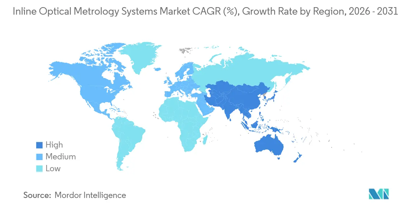
Asia-Pacific accounted for 54.67% of revenue in 2025 and is projected to expand at a 10.97% CAGR through 2031. South Korea and Taiwan host major advanced logic foundries and high-bandwidth memory production. Japan supports regional demand through semiconductor equipment and metrology capabilities. Nikon and NEDO announced a high-precision wafer-alignment metrology initiative in 2025 for next-generation semiconductor manufacturing. China adds demand from display-panel and solar thin-film production, supporting the Inline Optical Metrology Systems Market, even where export controls constrain leading-edge metrology.
North America is adding semiconductor capacity through the CHIPS and Science Act funding pipeline. Intel Fab 52 in Chandler, Arizona, entered high-volume manufacturing at the 18A node in the first quarter of 2026. TSMC’s Phoenix Fab 21 Phase 1 operates in volume production at N4, and Phase 2 is ramping at N3. TSMC’s March 2025 investment announcement supports a long-term U.S. equipment demand pipeline. Canada and Mexico add demand through precision engineering, automotive production, and battery manufacturing, favoring confocal and machine-vision systems.
Europe has demand from equipment producers and industrial users. Germany, the Netherlands, and France are home to JENOPTIK, ASML, Carl Zeiss, and Bruker. JENOPTIK reported an 85.3% year-on-year increase in Semiconductor and Advanced Manufacturing order intake during the first half of 2026. South America, the Middle East, and Africa remain early-stage regions for the Inline Optical Metrology Systems Market, with demand concentrated in automotive components, medical devices, and solar panel production.

Competitive Landscape
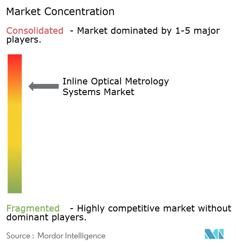
The Inline Optical Metrology Systems Market is moderately concentrated in high-end semiconductor applications and more fragmented in mid-tier industrial uses. Process-control specialists hold a strong position because they have deep application knowledge and large installed bases. Their service relationships create recurring revenue after equipment installation. Proprietary measurement libraries can be difficult for new suppliers to replicate. The result is a divide between vendors focused on advanced fabs and those serving automotive, battery, and precision-engineering customers.
Companies are expanding into adjacent measurement methods to address gaps in optical measurement. Onto Innovation announced a strategic partnership and a USD 710 million investment for a 27% minority stake in Rigaku Holdings in April 2026. The arrangement combines optical critical-dimension tools with CD-SAXS X-ray capabilities for sub-1 nm process control. JENOPTIK’s TRIOPTICS subsidiary introduced SurfInspect in January 2026 for automated surface-quality assessment under ISO 10110-7. These moves show how the Inline Optical Metrology Systems Market is using adjacent technologies and focused applications to maintain differentiation.
Compound semiconductor materials remain an opportunity because GaN and SiC need optical models based on non-silicon properties. Suppliers have not invested evenly in this capability. KLA’s semiconductor process-control business recorded USD 3.084 billion in revenue in the third quarter of fiscal 2026. New entrants need specialized applications, lower-cost platforms, or stronger analytics to compete effectively.
Inline Optical Metrology Systems Industry Leaders
KLA Corporation
ASML Holding N.V.
Onto Innovation Inc.
Applied Materials, Inc.
Carl Zeiss AG
- *Disclaimer: Major Players sorted in no particular order

Recent Industry Developments
- August 2026: JENOPTIK reported an 85.3% year-on-year increase in Semiconductor and Advanced Manufacturing order intake during H1 2026, driven by strong OEM demand for lithography and inspection in the semiconductor equipment sector. The company raised its full-year 2026 revenue outlook and expanded its EBITDA margin guidance to 20.0-21.0%.
- June 2026: Wooptix installed its Phemet® wavefront phase imaging metrology system at CEA-Leti's Grenoble cleanroom, with an installation date of May 4, 2026. The system enables sub-nanometer resolution nanotopography, warp, and bow measurement for advanced packaging and high-NA EUV lithography process development.
- May 2026: ASML received US Patent 12631975 for metrology systems with phased arrays for contaminant detection and microscopy, reflecting continued investment in optical metrology modality expansion for sub-nanometer semiconductor inspection.
- April 2026: Onto Innovation and Rigaku Holdings entered a strategic partnership and share purchase agreement under which Onto Innovation will acquire a 27% minority stake in Rigaku for USD 710 million. The arrangement integrates Onto's Ai Diffract™ software with Rigaku's CD-SAXS platforms to address a process control market estimated at more than USD 1 billion within 5 years at sub-1 nm nodes.


Global Inline Optical Metrology Systems Market Report Scope
Inline Optical Metrology Systems are high-speed, non-contact measurement solutions integrated directly into production lines to perform real-time, nanometer-precision analysis of critical dimensions, surface topography, and film thickness, enabling immediate process control and yield optimization in high-volume advanced manufacturing environments.
The Inline Optical Metrology Systems Market Report is Segmented by Offering (Hardware, Software and Analytics, and Services), Product Type (Optical Critical Dimension and Scatterometry Systems, Interferometric Profilometry and Film Thickness Systems, Chromatic Confocal and Laser Triangulation Systems, Machine Vision and Structured Light Systems, Optical Sensors and Spectrometers, and Other Product Types), Measurement Parameter (Critical Dimension and Profile, Film Thickness and Composition, Overlay, Alignment, and Registration, Surface Topography, Roughness, and Flatness, Defects and Particles, and Stress, Strain, Warp, and Bow), End-User Industry (Semiconductors and Advanced Packaging, Flat-Panel Displays and Optoelectronics, Automotive and Electric Vehicles, Battery Cells, Modules, and Packs, Aerospace and Defense, Medical Devices, Precision Engineering and Industrial Manufacturing, Solar, Glass, and Thin-Film Manufacturing, and Other End-User Industry), and Geography (North America, South America, Europe, Asia-Pacific, Middle East and Africa). The Market Forecasts are Provided in Terms of Value (USD).
| Hardware |
| Software and Analytics |
| Services |
| Optical Critical Dimension and Scatterometry Systems |
| Interferometric Profilometry and Film Thickness Systems |
| Chromatic Confocal and Laser Triangulation Systems |
| Machine Vision and Structured Light Systems |
| Optical Sensors and Spectrometers |
| Other Product Types |
| Critical Dimension and Profile |
| Film Thickness and Composition |
| Overlay, Alignment, and Registration |
| Surface Topography, Roughness, and Flatness |
| Defects and Particles |
| Stress, Strain, Warp, and Bow |
| Semiconductors and Advanced Packaging |
| Flat-Panel Displays and Optoelectronics |
| Automotive and Electric Vehicles |
| Battery Cells, Modules, and Packs |
| Aerospace and Defense |
| Medical Devices |
| Precision Engineering and Industrial Manufacturing |
| Solar, Glass, and Thin-Film Manufacturing |
| Other End-User Industry |
| North America | United States |
| Canada | |
| Mexico | |
| South America | Brazil |
| Argentina | |
| Rest of South America | |
| Europe | Germany |
| United Kingdom | |
| France | |
| Italy | |
| Spain | |
| Rest of Europe | |
| Asia-Pacific | China |
| Japan | |
| India | |
| South Korea | |
| Rest of Asia-Pacific | |
| Middle East and Africa | Middle East |
| Africa |
| By Offering | Hardware | |
| Software and Analytics | ||
| Services | ||
| By Product Type | Optical Critical Dimension and Scatterometry Systems | |
| Interferometric Profilometry and Film Thickness Systems | ||
| Chromatic Confocal and Laser Triangulation Systems | ||
| Machine Vision and Structured Light Systems | ||
| Optical Sensors and Spectrometers | ||
| Other Product Types | ||
| By Measurement Parameter | Critical Dimension and Profile | |
| Film Thickness and Composition | ||
| Overlay, Alignment, and Registration | ||
| Surface Topography, Roughness, and Flatness | ||
| Defects and Particles | ||
| Stress, Strain, Warp, and Bow | ||
| By End-User Industry | Semiconductors and Advanced Packaging | |
| Flat-Panel Displays and Optoelectronics | ||
| Automotive and Electric Vehicles | ||
| Battery Cells, Modules, and Packs | ||
| Aerospace and Defense | ||
| Medical Devices | ||
| Precision Engineering and Industrial Manufacturing | ||
| Solar, Glass, and Thin-Film Manufacturing | ||
| Other End-User Industry | ||
| By Geography | North America | United States |
| Canada | ||
| Mexico | ||
| South America | Brazil | |
| Argentina | ||
| Rest of South America | ||
| Europe | Germany | |
| United Kingdom | ||
| France | ||
| Italy | ||
| Spain | ||
| Rest of Europe | ||
| Asia-Pacific | China | |
| Japan | ||
| India | ||
| South Korea | ||
| Rest of Asia-Pacific | ||
| Middle East and Africa | Middle East | |
| Africa | ||


Key Questions Answered in the Report
What is the size of the Inline Optical Metrology Systems Market?
The market was valued at USD 4.15 billion in 2025 and is estimated to reach USD 6.72 billion by 2031, at an 8.64% CAGR.
Which end-user segment leads demand for inline optical metrology systems?
Semiconductors and advanced packaging led with 47.83% of end-user revenue in 2025, supported by tighter process-control needs.
Which offering is projected to expand fastest through 2031?
Software and analytics is projected to expand at an 11.27% CAGR, supported by AI-enabled recipe development and fleet management.
Why are battery manufacturers adopting inline optical inspection?
Battery production needs continuous checks on electrode thickness, geometry, and assembly quality to support energy density, safety, and automotive compliance.
Which region is expected to expand fastest through 2031?
Asia-Pacific is projected to expand at a 10.97% CAGR, supported by semiconductor capacity in South Korea, Taiwan, Japan, and China.
What limits wider adoption of inline optical metrology systems?
Equipment prices of USD 5 million to USD 20 million or more, retrofit work, and integration complexity can delay projects outside leading manufacturing sites.
Page last updated on:


 Your data is secure and never sold or shared.


