Optical Profilometry Systems Market Size and Share
Market Overview
| Study Period | 2020 - 2031 |
|---|---|
| Market Size (2026) | USD 690.08 Million |
| Market Size (2031) | USD 991.61 Million |
| Growth Rate (2026 - 2031) | 7.52 % |
| Fastest Growing Market | Asia-Pacific |
| Largest Market | Asia-Pacific |
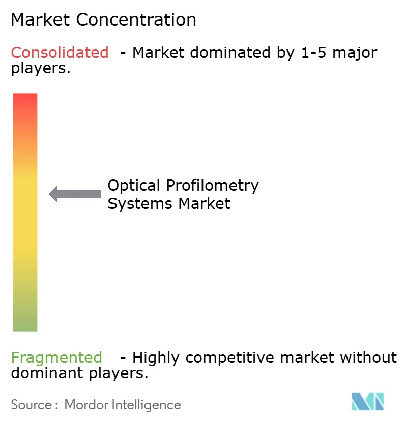
| Market Concentration | Medium |
Major Players *Disclaimer: Major Players sorted in no particular order Image © Mordor Intelligence. Reuse requires attribution under CC BY 4.0. | |
Optical Profilometry Systems Market Analysis by Mordor Intelligence
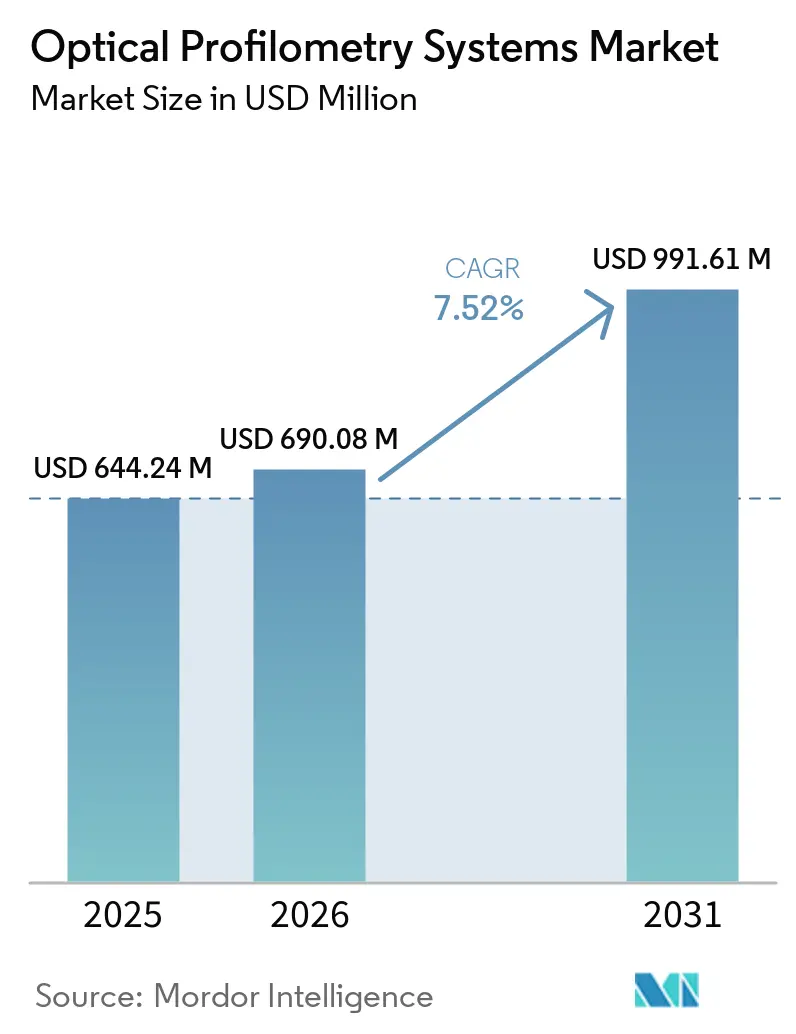
The optical profilometry systems market size was valued at USD 644.24 million in 2025 and estimated to expand from USD 690.08 million in 2026 to reach USD 991.61 million by 2031, at a CAGR of 7.52% during the forecast period (2026-2031). Demand in the global optical profilometry systems market is moving beyond metrology laboratories as advanced semiconductor packaging, EV battery production, and non-destructive in-line inspection create more production uses for optical profilometry systems. Semiconductor manufacturers in the optical profilometry systems market are adopting multi-system optical metrology suites as heterogeneous integration and high-bandwidth memory stacks raise inspection requirements. The 2025 order for 27 Bruker systems showed that white light interferometry tools have become part of production equipment for AI chip manufacturing. Within the optical profilometry systems market, high system costs, data-format interoperability limits, and competition from stylus instruments, scanning electron microscopes, and atomic force microscopes still limit adoption in selected applications. For the optical profilometry systems market, updated ISO 25178 standards have strengthened traceability for confocal chromatic, phase shifting interferometry, and point autofocus probe instruments, which can simplify qualification in regulated settings.
Key Report Takeaways
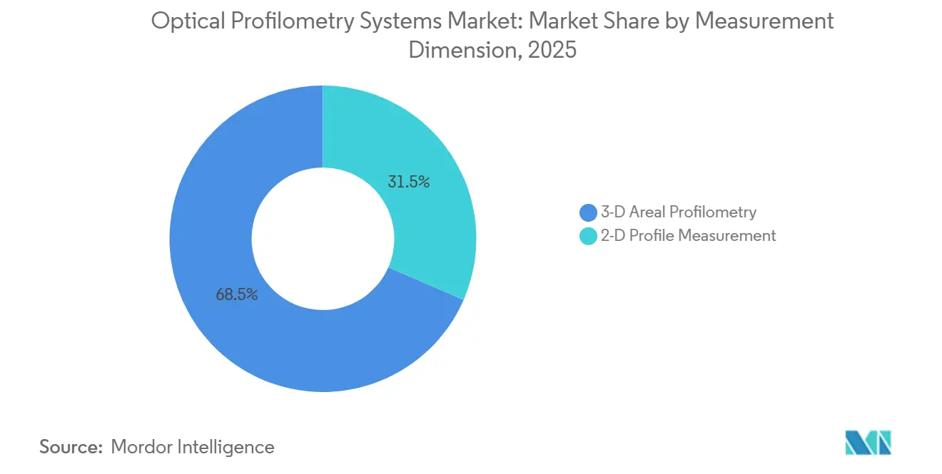
- By measurement dimension, 3-D areal profilometry held 68.47% of the optical profilometry systems market share in 2025, while 2-D profile measurement is projected to expand at an 8.14% CAGR through 2031.
- By form factor, benchtop and laboratory systems accounted for 52.73% of market share in 2025, while in-line and on-machine systems are projected to expand at a 7.88% CAGR through 2031.
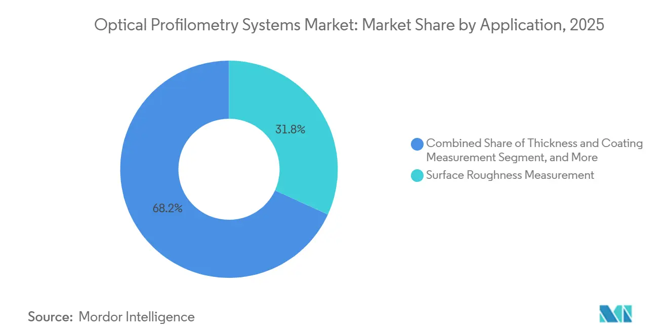
- By application, surface roughness measurement held 31.84% of the optical profilometry systems market share in 2025, while defect characterization and failure analysis are projected to expand at an 8.22% CAGR through 2031.
- By end-user industry, semiconductor and electronics held 34.67% of market share in 2025 and remained both the largest and fastest-growing end-user segment through 2026 with a CAGR of 8.92%
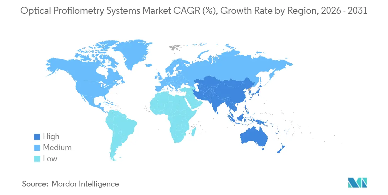
- By geography, Asia-Pacific held 39.26% of the market share in 2025 and is projected to expand at an 8.26% CAGR through 2031.
Note: Market size and forecast figures in this report are generated using Mordor Intelligence’s proprietary estimation framework, updated with the latest available data and insights as of January 2026.
Global Optical Profilometry Systems Market Trends and Insights
Drivers Impact Analysis*
| Driver | (~) % Impact on CAGR Forecast | Geographic Relevance | Impact Timeline |
|---|---|---|---|
| Semiconductor Miniaturization and Advanced Packaging | +2.1% | Asia-Pacific, North America, Europe | Short term (≤ 2 years) |
| Shift Toward Non-Contact 3-D Surface Measurement | +1.7% | Global | Medium term (2-4 years) |
| In-Line Metrology and Smart Manufacturing Integration | +1.4% | Asia-Pacific, North America, Europe | Medium term (2-4 years) |
| EV Battery Electrode and Coating Quality Control | +1% | Asia-Pacific, North America, Europe | Short term (≤ 2 years) |
| Medical Device Surface-Finish Traceability | +0.6% | North America, Europe | Medium term (2-4 years) |
| Optical Profilometry for Quantum and Photonic Hardware | +0.3% | North America, Europe, Asia-Pacific | Long term (≥ 4 years) |
| Source: Mordor Intelligence | |||
Semiconductor Miniaturization and Advanced Packaging
Advanced packaging is a central demand source in the optical profilometry systems market because it uses 2.5-D interposers, fan-out wafer-level packaging, and high-bandwidth memory stacks with demanding surface measurement needs. These designs require measurement of redistribution layer line widths below 2 µm, copper pillar coplanarity, and photoresist-through-film height. Contact stylus tools and 2-D scanning approaches do not address these tasks across complete die fields. White light interferometry can measure these surfaces in a single pass with the vertical resolution needed for advanced packaging.[1]KLA Corporation, “Zeta-388 3D Non-Contact Profilers,” KLA Instruments, kla.com Bruker’s 2025 order for 27 semiconductor optical metrology systems reflected faster purchasing cycles for AI chip production. Leading foundries operating sub-3 nm logic lines need rapid deployment, SECS/GEM integration, and repeatable measurements in high-throughput environments.
Shift Toward Non-Contact 3-D Surface Measurement
Manufacturers across the optical profilometry systems market are moving from sampled-line inspection toward full-surface characterization without contact. This shift allows surface information to be captured across an entire part rather than along an individual trace. ISO updated several ISO 25178 instrument standards in February 2025, covering confocal chromatic, interferometric, and point autofocus probe systems.[2]International Organization for Standardization, “ISO 25178-602:2025, Geometrical Product Specifications, Surface Texture: Areal, Part 602,” International Organization for Standardization, iso.org A stored areal dataset can be evaluated again using different parameters without physical access to the original component. This is useful for precision tooling and quantum hardware, where parts can be unique or expensive to measure again. Coherence scanning interferometry can capture turbine blade roughness, cooling-hole geometry, and form deviation in a single setup.
In-Line Metrology and Smart Manufacturing Integration
In-line optical profilometry places measurement within a production cell instead of sending parts to an offline room. This arrangement gives manufacturers feedback that can support process adjustments during production. Chromatic confocal sensors have been used on battery electrode coating lines to detect drying onset and changes in surface roughness at belt speeds not suited to contact measurement. Manufacturing systems also require metrology equipment to provide digital data that can connect with manufacturing execution systems. Ethernet-enabled sensor architectures can support those standardized data streams and operate at speeds up to 5 Gbit/s. The optical profilometry systems market benefits when manufacturers can link surface measurement to scrap reduction and faster process control across large-volume facilities.
EV Battery Electrode and Coating Quality Control
In the optical profilometry systems market, electrode surface roughness affects electrochemical activity, adhesion uniformity, contact resistance, and heat dissipation in battery production. These characteristics can influence cell energy density, cycle life, and safety. Non-contact 3-D techniques can measure electrodes, separators, and module housing components without damaging the sample. They can support defect classification and loading control across a wider surface than single-point systems. Dual-sided chromatic confocal measurement can capture top and bottom profiles at the same time, allowing thickness variation and coating homogeneity to be calculated at coating-station speeds.[3]Mohacsi et al., “In-Line Monitoring of a Multi-Stage Drying Process for Battery Electrodes: Vol. 2, Advancing Measurement Techniques with Chromatic Confocal Sensors,” European Physical Journal Special Topics, link.springer.com Battery projects in Europe and North America are placing this capability at the coating stage because surface quality at that stage affects subsequent cell assembly.
Restraints Impact Analysis*
| Restraint | (~) % Impact on CAGR Forecast | Geographic Relevance | Impact Timeline |
|---|---|---|---|
| High Capital Cost and Cost-Per-Part Uncertainty | -1.5% | Global, acute in South America and Middle East and Africa | Medium term (2-4 years) |
| Competition From SEM, AFM, Stylus, and Other Metrology | -1% | Global | Long term (≥ 4 years) |
| Shortage of Specialized Metrology Talent | -0.7% | Global | Medium term (2-4 years) |
| Limited Interoperability of Areal Texture Data | -0.4% | Global | Long term (≥ 4 years) |
| Source: Mordor Intelligence | |||
High Capital Cost and Cost-Per-Part Uncertainty
High-end 3-D platforms require an initial capital outlay that can be difficult for small and mid-size manufacturers to absorb. The cost per measured part also depends on equipment amortization, service contracts, and qualified operator time. This makes costs harder to model in facilities that produce a variable mix of parts. Pricing is often not transparent, and users can encounter additional costs for fixturing, vibration isolation, and software licenses after deployment. Limited local service capacity in South America and sub-Saharan Africa can turn an unplanned outage into several days of interrupted inspection. Modular sensor designs and leasing models can improve access, but they do not remove uncertainty around total ownership costs in price-sensitive operations.
Competition From SEM, AFM, Stylus, and Other Metrology
Atomic force microscopy and scanning electron microscopy retain advantages when users need sub-nanometer vertical resolution, subsurface imaging, or measurement of very steep slopes. These methods can offer performance that optical profilometry does not match at the same throughput-to-cost relationship. Stylus profilometers also remain relevant where contact measurements aligned with ISO 4287 profile standards are specified in contracts or regulations. Adoption of optical alternatives in these settings often requires a qualification process rather than a technical comparison alone. Research published in 2026 examined quantum-optimal surface roughness estimation using spatial mode demultiplexing. AI-based image analysis and quantum sensing are also changing the accuracy expectations applied to surface measurement methods.
*Our forecasts treat driver/restraint impacts as directional, not additive. The impact forecasts reflect baseline growth, mix effects, and variable interactions.
Segment Analysis
By Measurement Dimension: 3-D Areal Profilometry Leads While 2-D Profile Measurement Expands
3-D areal profilometry held 68.47% of the optical profilometry systems market share in 2025 because it characterizes complete surfaces in three dimensions. It supports wafer bow and warp measurement, medical implant surface validation, turbine blade roughness mapping, and other tasks that need complete surface datasets rather than single-line traces. Advanced semiconductor and precision-optics users have standardized areal measurement methods for demanding process and quality work. The optical profilometry systems market size associated with this approach is supported by its use where full-surface detail is required. Its position reflects mature-user needs and provides a reference point for users considering broader surface characterization and production deployment.
2-D profile measurement is projected to expand at an 8.14% CAGR from 2026 to 2031, as EV battery and thin-film solar producers use line-scan configurations for wide webs and large substrates. These users can adopt 2-D sensors before moving to full areal characterization, which reflects differences in production needs and measurement maturity. An integrated photonic surface profiler presented at OFC 2026 demonstrated 17 µm vertical accuracy and 30 µm lateral accuracy with a smaller system design. This work points to compact measurement options for constrained production settings. ISO 25178 provides parameters including Sa, Sq, and Sz for comparing and storing data from different instrument types, and the 2025 updates reinforced this framework across covered technologies.


By Form Factor: Laboratory Systems Lead While In-Line and On-Machine Systems Gain Use
Benchtop and laboratory systems held 52.73% of the optical profilometry systems market share in 2025, and research and quality laboratories remain the main deployment setting. These environments develop measurement and process recipes before they move into production. The installed base reflects long-term use in semiconductor process development, materials research, and precision optics characterization, where white light interferometry systems have been widely used. Laboratory systems provide the controlled setup required for detailed surface measurement. This base supports their continuing role in the optical profilometry systems market and in pre-production process evaluation.
In-line and on-machine systems are projected to expand at a 7.88% CAGR from 2026 to 2031 because real-time feedback can reduce scrap enough to support integration costs. These systems move inspection closer to the process that creates the part, while portable and hand-held systems serve maintenance, repair, overhaul, and large-part inspection. Portable chromatic confocal systems can support turbine blade checks and in-situ coating thickness verification when laboratory transport is impractical. KEYENCE launched the VK-X4000 Series in March 2026 with laser confocal, white light interferometry, focus variation, and automated multi-point measurement capabilities. The platform reflects demand for measurement versatility in laboratory and near-line settings.
By Application: Surface Roughness Measurement Leads While Defect Analysis Advances
Surface roughness measurement accounted for 31.84% of the optical profilometry systems market share in 2025 and is used in semiconductor wafer polishing, EV electrode coating, aerospace turbine vanes, and medical implant textures. This broad applicability makes it the largest application in the optical profilometry systems market. It is often the first use case for manufacturers adopting 3-D aerial measurement and can indicate how deeply optical methods have entered manufacturing processes. Roughness data supports quality requirements across precision surfaces and further demand for flatness, coating thickness, and form measurements. Its leading position rests on the range of industries that require repeatable characterization during routine manufacturing.
Defect characterization and failure analysis are projected to expand at an 8.22% CAGR from 2026 to 2031, as semiconductor yield programs identify and classify sub-micron surface anomalies. The results can support process improvement and yield recovery. Thickness and coating measurements are also gaining use in EV battery production, where in-line areal measurements can help control electrode mass-loading uniformity across the full width. Single-point sensors do not provide the same full-width view, while flatness and form measurement support non-contact evaluation of total thickness variation, bow, and warp. Step-height measurement, microfluidic channel characterization, and additive manufacturing surface validation add demand from research and pilot production.

By End-User Industry: Semiconductor and Electronics Sustains Demand
Semiconductor and electronics accounted for 34.67% of the optical profilometry systems market share in 2025 and remained the largest and fastest-growing end-user segment through 2026, with a CAGR of 8.92%. Advanced node scaling, heterogeneous integration, and AI accelerator chiplet production increase measurement requirements because each process node can introduce new measurement points per wafer and tighter tolerances. These conditions support non-contact surface metrology. The optical profilometry systems market size in semiconductor applications benefits from this concentration of production requirements. Leading platforms support SECS/GEM compatibility for 200 mm and 300 mm fab automation systems, thereby shortening deployment cycles in high-volume facilities.
Automotive and EV production creates demand because electrode surface quality affects lithium-ion cell yield and cycle life. Healthcare and medical devices require documented, traceable surface-finish measurement for implantable devices and surgical instruments under quality-system requirements. Aerospace and defense users apply portable and benchtop coherence scanning interferometry to cooling holes, coatings, and curved airfoil surfaces. Industrial manufacturing, energy, and power users measure roughness, flatness, and coating thickness on precision gears, hydraulic components, wind turbine blade edges, and solar metallization features. These end uses provide a broad base of demand for non-destructive measurement beyond semiconductor fabrication.
Geography Analysis
Asia-Pacific held 39.26% of the optical profilometry systems market share in 2025 and is projected to expand at an 8.26% CAGR from 2026 to 2031. Taiwan, South Korea, China, and Japan contain major advanced foundries and memory fabrication facilities with substantial yield-management requirements. TSMC’s N3 and N2 ramps, Samsung’s 3-D NAND and DRAM expansion, and SMIC’s capacity additions create tool purchase cycles for wafer characterization, advanced packaging inspection, and MEMS process control. Japan also serves as a supplier base, and KEYENCE’s VK-X4000 Series launch in 2026 reinforced the region’s role in demand and supply within the optical profilometry systems market. These conditions produce high-volume demand for non-contact surface metrology across the region.
North America and Europe form a second tier of demand for the optical profilometry systems market, with users in semiconductor equipment, aerospace, medical devices, and precision manufacturing. North America has semiconductor fabrication investment and a large installed base in aerospace maintenance and medical-device quality laboratories. Europe has precision manufacturing clusters in Germany, Switzerland, and the United Kingdom, with Bruker Alicona, Jenoptik, and Sensofar among established regional suppliers. Germany’s shift toward electric drivetrains supports battery electrode coating inspection and electric motor component measurement. This activity is beginning to reproduce the multi-station procurement model used in semiconductor production.
South America, the Middle East, and Africa represent a smaller but developing part of optical profilometry revenue, with localized demand from Brazil’s aerospace and mining-equipment sectors, Saudi Arabia’s petrochemical investments, and South Africa’s precision component supply chains. Benchtop laboratory systems address much of this demand, while high costs and limited local service capacity constrain broader penetration. Sensofar expanded its distributor network in North and Central America in 2025 through Visional Technologies and Midwest Metrology, showing a way to build local reach without a matching fixed-cost base. Future demand will depend on technology-transfer agreements, local manufacturing investment, and EV supply-chain extension into regional battery and automotive component production.

Competitive Landscape
The optical profilometry systems market is moderately consolidated in the high-performance tier, where vendors compete on speed, vertical resolution, technology integration, and application software rather than price alone. Established suppliers are developing platforms that combine interferometry, confocal microscopy, and focus variation, which reduces the number of instruments a laboratory or production line must maintain. These platforms also broaden the applications served by each system. KEYENCE’s VK-X4000 combines laser confocal, white light interferometry, focus variation, and automated multi-point scanning. Bruker Alicona’s µCMM NEO combines complementary optical technologies with five-axis kinematics in a single optical coordinate measuring machine.
SECS/GEM conformance is an advantage when a system is integrated into fab automation because replacing an installed platform can require requalification across connected process modules. Bruker’s InSight WLI supports SECS/GEM communication for 200 mm and 300 mm wafer handling, which can make supplier relationships more durable in fab environments. The optical profilometry systems market also has opportunities in quantum and photonic hardware characterization, where requirements extend beyond typical classical interferometry limits. Portable, field-deployable systems provide another entry point for aerospace maintenance and large-format industrial inspection. These areas create room for suppliers serving specialized use cases.
Sensofar Metrology and Nanovea use application-specific configurations and close engagement with niche users, which can help them compete with suppliers focused on large semiconductor and precision-optics accounts. AI-assisted surface-analysis software supports automated anomaly classification, recipe-free measurement, and digital twin integration. This software can reduce expertise needs for selected workflows and broaden use among process engineers and quality technicians. Vendor strategies in the optical profilometry systems market therefore address high-value applications and more accessible operating settings.
Optical Profilometry Systems Industry Leaders
Bruker Corporation
KLA Corporation
KEYENCE Corporation
Zygo Corporation
Mitutoyo Corporation
- *Disclaimer: Major Players sorted in no particular order

Recent Industry Developments
- March 2026: KEYENCE Corporation launched the VK-X4000 Series 3D Optical Profiling Microscope globally, combining laser confocal, white light interferometry, and focus variation in a single instrument with a maximum magnification of 28,800× and an automated multi-point measurement function. The platform eliminates manual reprogramming between sample positions, enabling faster throughput in industrial quality control and reducing dependence on specialist operators.
- March 2026: Bruker Alicona initiated the series rollout of the µCMM NEO, the next generation of its optical coordinate measuring machine, with initial customer deliveries scheduled for Q4 2026. The µCMM NEO integrates four complementary optical measurement technologies, including focus variation, WLI, and confocal, alongside five-axis kinematics, allowing dimensional inspection, form analysis, and surface characterization without changing instruments or setups. The first system was ordered by a customer in high-precision toolmaking and stamped-parts production.
- January 2026: ISO/FDIS 25178-71, Software Measurement Standards for Areal Surface Texture, was circulated as a Final Draft International Standard following the close of the DIS ballot in August 2025. The revision standardizes data file formats and software validation criteria for areal surface texture instruments, improving cross-vendor data interoperability and supporting multi-site measurement consistency in complex manufacturing environments.
- September 2025: Bruker Alicona launched the SensorX, a high-precision 3D metrology sensor developed for seamless OEM integration into cutting-tool preparation cells. Co-developed with Nagel Technologies GmbH, the SensorX enables autonomous edge preparation with real-time process correction and automated wear compensation in unmanned production environments, extending optical profilometry into closed-loop machining systems.


Global Optical Profilometry Systems Market Report Scope
The Optical Profilometry Systems Market comprises non-contact optical instruments that measure 3D surface topography, roughness, step height, texture, and thin-film characteristics at micro- to nanoscale resolution using techniques such as white-light interferometry (WLI), confocal microscopy, coherence scanning interferometry (CSI), and focus variation. These systems are widely used in semiconductors, precision optics, automotive, aerospace, medical devices, MEMS, and advanced materials for quality control, R&D, failure analysis, and process optimization.
The Optical Profilometry Systems Market Report is Segmented by Measurement Dimension (3-D Areal Profilometry, and 2-D Profile Measurement), Form Factor (Benchtop and Laboratory Systems, In-Line and On-Machine Systems, and Portable and Hand-Held Systems), Application (Surface Roughness Measurement, Thickness and Coating Measurement, Step Height Measurement, Flatness and Form Measurement, Defect Characterization and Failure Analysis, and Other Applications), End-User Industry (Semiconductor, Automotive and EV, Aerospace, Healthcare, Industrial, Energy, and Other End-User Industries), and Geography (North America, South America, Europe, Asia-Pacific, Middle East and Africa). The Market Forecasts are Provided in Terms of Value (USD).
| 3-D Areal Profilometry |
| 2-D Profile Measurement |
| Benchtop and Laboratory Systems |
| In-Line and On-Machine Systems |
| Portable and Hand-Held Systems |
| Surface Roughness Measurement |
| Thickness and Coating Measurement |
| Step Height Measurement |
| Flatness and Form Measurement |
| Defect Characterization and Failure Analysis |
| Other Applications |
| Semiconductor and Electronics |
| Automotive and Electric Vehicles |
| Aerospace and Defense |
| Healthcare and Medical Devices |
| Industrial Manufacturing |
| Energy and Power |
| Other End-User Industries |
| North America | United States | |
| Canada | ||
| Mexico | ||
| South America | Brazil | |
| Argentina | ||
| Rest of South America | ||
| Europe | Germany | |
| United Kingdom | ||
| France | ||
| Italy | ||
| Spain | ||
| Rest of Europe | ||
| Asia-Pacific | China | |
| Japan | ||
| India | ||
| South Korea | ||
| ASEAN | ||
| Rest of Asia-Pacific | ||
| Middle East and Africa | Middle East | Saudi Arabia |
| United Arab Emirates | ||
| Turkey | ||
| Rest of the Middle East | ||
| Africa | South Africa | |
| Nigeria | ||
| Rest of Africa | ||
| By Measurement Dimension | 3-D Areal Profilometry | ||
| 2-D Profile Measurement | |||
| By Form Factor | Benchtop and Laboratory Systems | ||
| In-Line and On-Machine Systems | |||
| Portable and Hand-Held Systems | |||
| By Application | Surface Roughness Measurement | ||
| Thickness and Coating Measurement | |||
| Step Height Measurement | |||
| Flatness and Form Measurement | |||
| Defect Characterization and Failure Analysis | |||
| Other Applications | |||
| By End-User Industry | Semiconductor and Electronics | ||
| Automotive and Electric Vehicles | |||
| Aerospace and Defense | |||
| Healthcare and Medical Devices | |||
| Industrial Manufacturing | |||
| Energy and Power | |||
| Other End-User Industries | |||
| By Geography | North America | United States | |
| Canada | |||
| Mexico | |||
| South America | Brazil | ||
| Argentina | |||
| Rest of South America | |||
| Europe | Germany | ||
| United Kingdom | |||
| France | |||
| Italy | |||
| Spain | |||
| Rest of Europe | |||
| Asia-Pacific | China | ||
| Japan | |||
| India | |||
| South Korea | |||
| ASEAN | |||
| Rest of Asia-Pacific | |||
| Middle East and Africa | Middle East | Saudi Arabia | |
| United Arab Emirates | |||
| Turkey | |||
| Rest of the Middle East | |||
| Africa | South Africa | ||
| Nigeria | |||
| Rest of Africa | |||


Key Questions Answered in the Report
What is the size of the optical profilometry systems market?
The optical profilometry systems market was valued at USD 644.24 million in 2025, is estimated at USD 690.08 million in 2026, and is forecast to reach USD 991.61 million by 2031 at a CAGR of 7.52%.
What is driving demand for optical profilometry systems?
Advanced semiconductor packaging, non-contact 3-D measurement, in-line metrology, and EV battery electrode quality control support adoption. These uses bring surface measurement into production environments rather than limiting it to metrology laboratories.
Which measurement dimension leads optical profilometry systems?
3-D areal profilometry held 68.47% share in 2025 because it captures complete surface datasets for demanding inspection work. Users apply it to semiconductor wafers, medical implant surfaces, and turbine blade roughness measurement.
Which form factor is expanding fastest through 2031?
In-line and on-machine systems are projected to expand at a 7.88% CAGR through 2031. Manufacturers adopt these systems when real-time process feedback can reduce scrap and support faster production adjustments.
Which application is expanding fastest through 2031?
Defect characterization and failure analysis is projected to expand at an 8.22% CAGR from 2026 to 2031. Semiconductor yield programs use these capabilities to identify sub-micron anomalies and support process improvement.
Which region has the strongest demand for optical profilometry systems?
Asia-Pacific held 39.26% share in 2025 and is projected to expand at an 8.26% CAGR through 2031. Major semiconductor and memory fabrication facilities in Taiwan, South Korea, China, and Japan support this position.
Why do semiconductor manufacturers use optical profilometry?
They use non-contact surface metrology for wafer characterization, advanced packaging inspection, and process control as tolerances become tighter. SECS/GEM integration also supports connections with 200 mm and 300 mm fab automation systems.
Page last updated on: