
High-K And CVD ALD Metal Precursors Market Size and Share
Market Overview
| Study Period | 2020 - 2031 |
|---|---|
| Market Size (2026) | USD 0.66 Billion |
| Market Size (2031) | USD 0.91 Billion |
| Growth Rate (2026 - 2031) | 6.55 % |
| Fastest Growing Market | Asia Pacific |
| Largest Market | Asia Pacific |
| Market Concentration | Medium |
Major Players
*Disclaimer: Major Players sorted in no particular order Image © Mordor Intelligence. Reuse requires attribution under CC BY 4.0. |
|
High-K And CVD ALD Metal Precursors Market Analysis by Mordor Intelligence
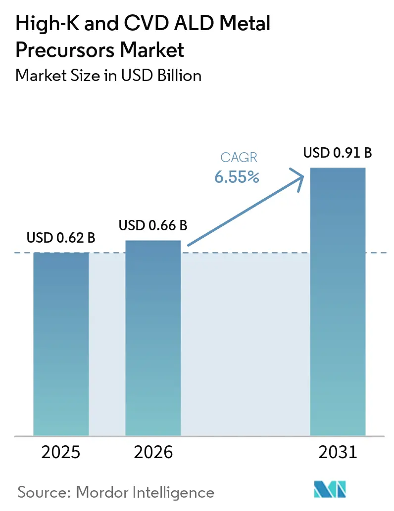
The High-K and CVD ALD metal precursors market size is expected to increase from USD 0.62 billion in 2025 to USD 0.66 billion in 2026 and reach USD 0.91 billion by 2031, growing at a CAGR of 6.55% over 2026-2031. Robust demand stems from the transition to 2-nanometer gate-all-around logic, 500-plus-layer 3D NAND stacks, and EUV-patterned DRAM trench capacitors, all of which consume markedly higher volumes of hafnium, tungsten, and zirconium chemistries per wafer. Fab clusters in Korea, Taiwan, China, and the United States are collectively investing more than USD 200 billion in new capacity and are mandating on-site precursor blending to cut delivery lead times. Suppliers able to guarantee sub-ppm impurity levels, ISO 9001 traceability, and PFAS-free formulations are securing long-term supply agreements, while niche innovators targeting ruthenium and molybdenum interconnects are carving out high-margin niches. Headline risks include hafnium metal tightness, evolving environmental rules on alkyl-amide ligands, and the capital intensity of solid-precursor sublimation tools.
Key Report Takeaways
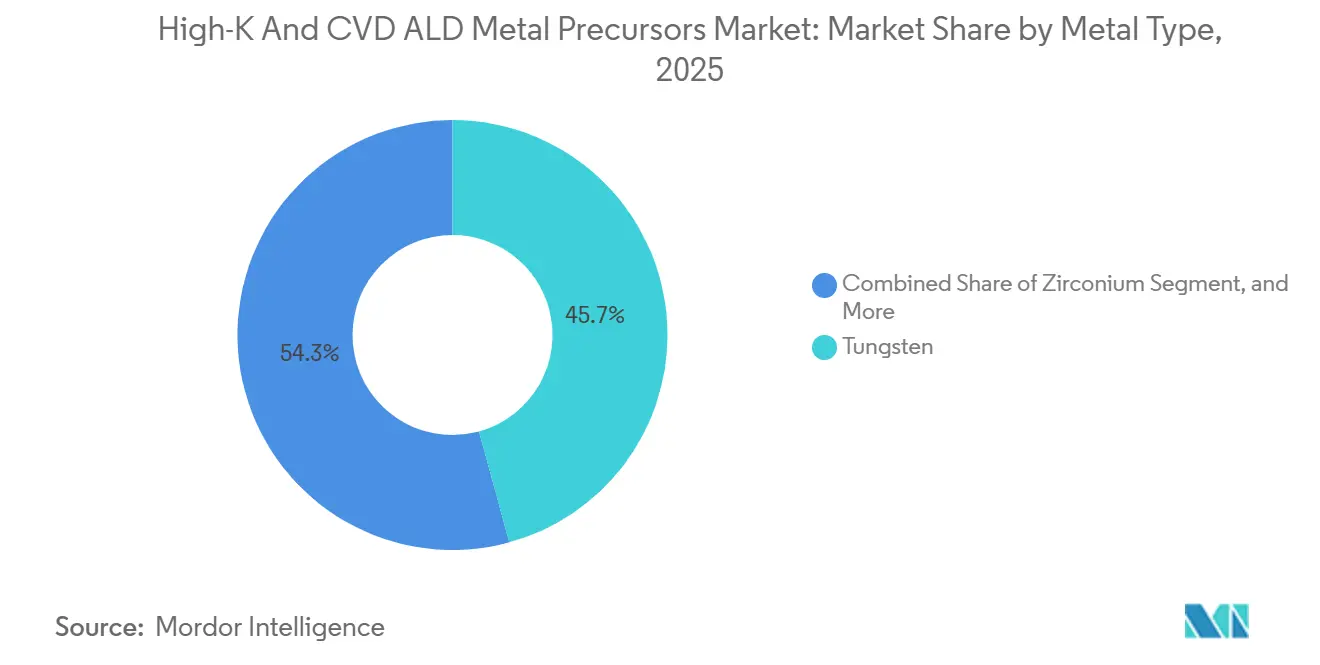
- By metal type, tungsten captured 45.74% of 2025 revenue, while zirconium precursors are projected to expand at a 6.98% CAGR through 2031.
- By deposition method, thermal ALD led with 48.19% share in 2025, whereas plasma-enhanced ALD is forecast to post the fastest growth at 7.11% CAGR to 2031.
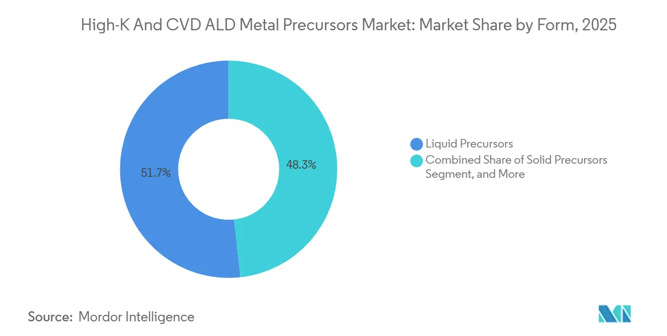
- By form, liquid chemistries accounted for 51.73% of the 2025 value, yet solid precursors are advancing at a 6.91% CAGR on purity and waste-reduction advantages.
- By end use, logic devices held a 38.18% share in 2025, and emerging memories are expected to grow the fastest at a 6.94% CAGR through 2031.
- By geography, Asia-Pacific accounted for 60.28% of 2025 revenue and is the fastest-growing region, with a 7.21% CAGR over the forecast period.
Note: Market size and forecast figures in this report are generated using Mordor Intelligence’s proprietary estimation framework, updated with the latest available data and insights as of January 2026.
Market Trends and Insights
Drivers Impact Analysis of High-K And CVD ALD Metal Precursors Market*
| Driver | (~) % Impact on CAGR Forecast | Geographic Relevance | Impact Timeline |
|---|---|---|---|
| Mainstream Scaling To <3 Nm Logic Nodes | +2.1% | Taiwan, South Korea, United States | Medium term (2-4 years) |
| 3D-NAND ≥256 Layers | +1.8% | China, South Korea, Japan | Medium term (2-4 years) |
| EUV-Patterned DRAM Trench Capacitors | +1.4% | South Korea, Taiwan | Short term (≤2 years) |
| Rising Chinese And Korean Fab Capacity | +1.2% | China, Korea | Long term (≥4 years) |
| Ferroelectric HfZrO Memory Adoption | +0.9% | Global | Long term (≥4 years) |
| Remote-Plasma-ALD For Leakage Control | +0.7% | South Korea, Taiwan, China | Medium term (2-4 years) |
| Source: Mordor Intelligence | |||
Mainstream Scaling to Sub-3 nm Logic Nodes
Gate-all-around nanosheet designs at 2-nanometer nodes consume 35-50% more high-k dielectric per wafer than 3-nanometer FinFETs because wrap-around gates and backside power networks double the number of ALD cycles required. TSMC’s N2 logic, in volume production since late 2025, deposits hafnium oxide on both sides of the device stack, while Intel’s 18A PowerVia flow adds tungsten through-silicon vias to the precursor bill of materials.[1] The resulting spike in precursor intensity is magnified by yield-learning overruns that force fabs to over-provision materials during early ramps.
Layer-by-Layer Control for Backside Power Delivery
Backside power routes require ruthenium or tungsten atomic layer deposition (ALD) on through-silicon vias (TSVs) with diameters less than 500 nanometers. These materials are critical because they can maintain performance at such small scales. Intel’s 18A node specifically selected ruthenium because of its low resistivity, which minimizes energy loss, and its superior electromigration resistance, which enhances durability under high current densities. Additionally, research from Imec highlights that adopting backside power routing can reduce on-chip voltage droop by approximately 25%, improving overall power delivery efficiency. However, while this layout significantly reduces IR drop, it also increases the cost of per-wafer precursor materials by an estimated 40%, presenting a trade-off between performance gains and manufacturing expenses.
3D NAND Stacks Above 500 Layers
Every layer added to a 3D NAND string requires two ALD passes, meaning that as the number of layers increases from 200 to 500, the demand for precursor volumes grows 1.5 times faster than the growth in wafer starts. This highlights the significant impact of layer scaling on material consumption. In 2024, SK hynix successfully shipped 321-layer parts and has set a target to achieve 400-layer parts by late 2026. This progression indicates that each wafer will require more than 800 ALD cycles, reflecting the increasing complexity of manufacturing processes. According to SEMI data, NAND precursor usage is projected to grow by 28% in 2025, compared to a 12% growth in wafer starts. This disparity underscores the multiplier effect, in which advances in layer technology drive a disproportionate increase in material requirements.
EUV-Patterned High-Aspect-Ratio DRAM Capacitors
Shrinking trench pitches below 30 nanometers has led to aspect ratios exceeding 70:1, creating a geometry that only plasma-enhanced Atomic Layer Deposition (ALD) can effectively coat without voids. This advanced coating technique ensures uniformity and precision in high-aspect-ratio structures. Researchers at KAIST achieved 98% step coverage with 100 MHz remote plasma, demonstrating this technology's ability to address complex geometries. Additionally, Samsung’s latest DDR5 node implementation has increased ALD cycle counts by 35%, highlighting the growing adoption of plasma-enhanced ALD in advanced semiconductor manufacturing processes.
Restraints Impact Analysis of High-K And CVD ALD Metal Precursors Market*
| Restraint | (~) % Impact on CAGR Forecast | Geographic Relevance | Impact Timeline |
|---|---|---|---|
| Hafnium Metal Supply Constraints | -0.7% | North America and Europe | Short term (≤ 2 years) |
| Escalating EHS Rules on Alkyl-Amide and PFAS | -0.5% | Europe and North America | Medium term (2-4 years) |
| Capex Intensity of Solid-Precursor Systems | -0.4% | Global | Medium term (2-4 years) |
| Plasma Damage Narrowing PE-ALD Windows | -0.3% | Global | Short term (≤ 2 years) |
| Source: Mordor Intelligence | |||
Hafnium Metal Supply Constraints and Price Volatility
Hafnium output, which is intrinsically linked to zirconium mining, remained limited to only 80-90 metric tons in 2025. However, the demand for hafnium precursors is projected to exceed 120 metric tons by 2028, creating a significant supply-demand gap. This imbalance has driven spot prices to surge, reaching USD 1,400 per kilogram in the first quarter of 2026. The rising prices have compelled semiconductor fabs to increase their inventories and maintain higher safety stocks to mitigate supply risks. Although new separation capacity in Western Australia is expected to add 15-20 metric tons by 2027, this increase will address only a fraction of the anticipated shortfall, leaving the market under pressure to meet growing demand.
Escalating EHS Regulations on Alkyl-Amide and PFAS Ligand Chemistries
The European Chemicals Agency (ECHA) and the US Environmental Protection Agency (EPA) have proposed classifying several per- and polyfluoroalkyl substances (PFAS) ligands as hazardous materials. This regulatory shift has prompted precursor reformulations, which are expected to increase abatement and qualification costs by approximately USD 0.15-0.25 per wafer.[2] In response to these changes, Merck KGaA is actively working on converting 12 of its products to PFAS-free variants. However, this transition is a complex process that can take up to 24 months to complete, including customer re-qualification to ensure compliance with and performance standards. According to SEMI, an industry association, around 30-40% of current atomic layer deposition (ALD) chemistries lack a technically equivalent PFAS-free alternative, posing significant challenges for the industry in adapting to these regulatory requirements.
*Our forecasts treat driver/restraint impacts as directional, not additive. The impact forecasts reflect baseline growth, mix effects, and variable interactions.
High-K And CVD ALD Metal Precursors Market Segment Analysis
By Metal Type:
Volume Leadership of Tungsten Faces Zirconium and Ruthenium UpsideTungsten-based chemistries accounted for the largest share with 45.74% in 2025 value, and that dominance rests on their entrenched role in contact plugs and word-lines, where low resistivity and high modulus are vital. The High-K and Chemical Vapor Deposition (CVD) Atomic Layer Deposition (ALD) metal precursors market for tungsten applications accounted for nearly half of overall revenue in 2025, reflecting widespread integration in both logic and memory stacks. Ruthenium, however, is gaining mindshare because its resistivity remains favorable at sub-5-nanometer thicknesses, and new liquid precursors now deliver stable vapor pressures above 100 torr. Zirconium’s 6.98% CAGR shows how ferroelectric HfZrO dielectrics are reshaping embedded memory flows.
Looking forward, zirconium’s share acceleration could edge into tungsten territory as foundries deploy FeFETs across microcontroller nodes. Hafnium remains a strategic metal because every sub-7 nanometer gate dielectric relies on it, yet its supply chain is structurally tight. Ruthenium’s emergence in backside power rail liners, validated by PowerVia risk production, points to a disruptive mix shift. Cobalt and molybdenum occupy niche but growing roles as barrier-liner substitutes, while aluminum oxide stays relevant for mature analog and power devices.

By Deposition Method:
Plasma-Enhanced ALD Continues to Gain MomentumThermal ALD retained the largest market share at 48.19% in 2025, thanks to its simplicity, but plasma-enhanced ALD’s 7.11% CAGR highlights how aspect-ratio pressures are rewriting tool roadmaps. The High-K and CVD ALD metal precursors market size for plasma-enhanced processes is on track to overtake thermal revenue late in the forecast window as DRAM trenches and backside vias both demand remote-plasma chemistries. Very-high-frequency plasma sources cut ion damage in half compared with 13.56 MHz systems, broadening the process window for sensitive low-k stacks.
Metal-organic CVD still underpins thick tungsten fills and aluminum pads because its 5-10 nanometer-per-minute deposition rates keep the cost-per-wafer low for high-volume structures. Spatial ALD and hybrid ALD-CVD flows remain minority shares but are attracting display, solar, and advanced packaging users who value the advantages of continuous motion or sequential nucleation. Intel’s public disclosure of a hybrid ALD-seed plus CVD-bulk tungsten approach for 18A vias signals broader acceptance of these mixed regimes.[3]
By Form:
Liquid Precursors Hold the Majority but Solid Variants Climb on PurityLiquid bubbler systems accounted for just over half of the revenue in 2025, specifically 51.73%, due to the optimization of existing fab plumbing around these systems. Their stable vapor pressures, typically 0.5-2.0 torr, make flow control straightforward and reliable. However, solid sublimation technology is advancing rapidly, with the High-K and CVD ALD metal precursors market share for solid forms steadily increasing. This growth is supported by a 6.91% CAGR in spending, driven by advantages such as impurity levels below 10 ppb and the elimination of significant solvent waste, which makes these solutions more environmentally friendly and efficient.
Despite these advancements, tool costs remain a significant challenge. Solid delivery modules can cost over USD 2 million, presenting a substantial capital expenditure. However, leading-edge fabs are increasingly finding that the yield savings and operational efficiencies provided by these systems outweigh the initial investment. Gas-phase chemistries, such as tungsten hexafluoride, continue to maintain their strong position in CVD applications, particularly where high throughput is critical. Additionally, collaborations like the partnership between Gelest and IBM on dry-resist EUV precursors suggest that gas and solid chemistries may increasingly converge in lithography and deposition applications, further expanding their potential use cases and market opportunities.
By End-Use Application:
Logic Dominates Value, Emerging Memories Propel GrowthLogic captured the largest share with 38.18% in 2025 slice because sub-3-nanometer nodes require dual-sided gate stacks and backside power, effectively doubling the precursor load per wafer. This demand has positioned logic as a dominant segment, with the High-K and CVD ALD metal precursors market size for logic alone already exceeding USD 0.23 billion. Additionally, emerging memory technologies such as FeFETs, RRAM, and MRAM are experiencing rapid growth, representing the fastest-growing segment with a compound annual growth rate (CAGR) of 6.94% during the forecast period.
DRAM remains the second-largest consumer of High-K and CVD ALD metal precursors, driven by advancements in EUV trench scaling, which have increased plasma-enhanced ALD cycles by more than one-third. Meanwhile, 3D NAND accounts for approximately 20% of the market value. However, its layer-count roadmap suggests it will contribute a disproportionately large share of incremental volume in the coming years. Interconnect and metallization layers continue to demand materials such as ruthenium, cobalt, and molybdenum liners to ensure reliability and performance. Furthermore, analog, power, and specialty flows maintain a stable niche, supported by automotive qualification cycles and the ability to operate within wider thermal budgets.
Geography Analysis
APAC High-K and CVD ALD Metal Precursors Market
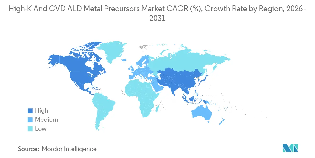
Asia-Pacific dominates value with a 60.28% hold in 2025, reflecting massive wafer capacity across Korea, Taiwan, and China. Regional fab investments exceeding USD 200 billion between 2024-2026 underpin a 7.21% CAGR to 2031. Samsung’s restarted P5 project and SK hynix’s advanced Yongin timeline force suppliers to pre-position inventory on site, while YMTC and CXMT accelerate expansions to counter export controls. Strong policy support, labor availability, and entrenched ecosystems allow the Asia-Pacific to maintain cost advantages despite a rising local wage base.
North America High-K and CVD ALD Metal Precursors Market
North America accounted for close to 19% of 2025 revenue and is on track for roughly a 7% CAGR as CHIPS Act incentives trigger at least 23 new fabs or expansions. TSMC Arizona, Intel Ohio, and Samsung Texas collectively require localized hafnium and tungsten purification plants to satisfy domestic-content mandates. Air Liquide, Entegris, and SK Materials are already breaking ground on gas and precursor campuses adjacent to these megaprojects.[4]
EMEA and South America High-K and CVD ALD Metal Precursors Market
Europe controls about 11% of 2025 spend, buoyed by Intel Magdeburg and STMicroelectronics Crolles expansions. Regional growth hovers near 6% CAGR as automotive demand and sovereignty initiatives lock in subsidies. The Middle East, Africa, and South America remain sub-5% combined, yet Brazilian automotive fabs and Israeli defense nodes present high-margin specialty opportunities. Across all regions, dual sourcing and shorter lead-times shift competitive advantage toward suppliers operating multiple ISO-certified plants.
Competitive Landscape
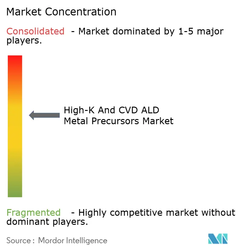
Market concentration is moderate: the five largest players account for an estimated 50-55% of global revenue. Air Liquide leads in vertical integration, investing EUR 924 million (USD 997 million) during Q3 2025 alone across Germany, Singapore, and the United States. Merck KGaA expands in Korea, while Entegris leverages CHIPS Act grants to scale US precursor lines. Soulbrain, Hansol Chemical, and SK Materials gain share in Asia-Pacific by bundling delivery systems with online purity monitoring, cutting fab qualification from 18 to 12 months.
Disruptors are targeting ruthenium, molybdenum, and PFAS-free chemistries. TANAKA’s TRuST liquid delivers 1.7 angstrom per cycle ALD rates at vapor pressures 100 times those of previous formulations, opening backside power and DRAM electrode opportunities. Chinese supplier Jiangsu Yoke grew 72% year-over-year in 2024 by pricing 30-40% below Western incumbents and guaranteeing 12-hour delivery inside the Yangtze River Delta. Competitive dynamics increasingly reward the ability to co-develop precursor-plus-hardware packages that de-risk integration for foundries.
Fab operators are enforcing stringent dual-source rules, compelling suppliers to clone each product at a second plant and to validate interchangeability. Those requirements raise the working capital bar for smaller firms, yet they also create opportunities for niche specialists who can qualify novel precursors in 9 months rather than the legacy 18-month cycle. White-space exists in solid-state hafnium lines and in ligand systems compliant with upcoming PFAS prohibitions.
High-K And CVD ALD Metal Precursors Industry Leaders
-
Air Liquide S.A.
-
ADEKA Corporation
-
Merck KGaA
-
Entegris Inc.
-
SK Materials Co., Ltd.
- *Disclaimer: Major Players sorted in no particular order
High-K And CVD ALD Metal Precursors Market Companies Covered in this Report
- Air Liquide S.A.
- ADEKA Corporation
- Merck KGaA
- Entegris Inc.
- Hansol Chemical Co., Ltd.
- DNF Co., Ltd.
- Soulbrain Co., Ltd.
- UP Chemical Co., Ltd.
- Tanaka Kikinzoku Kogyo K.K.
- Strem Chemicals, Inc.
- Versum Materials LLC
- SK Trichem Co., Ltd.
- SK Materials Co., Ltd.
- Gelest, Inc.
- Air Products and Chemicals, Inc.
- Jiangsu Yoke Technology Co., Ltd.
- Solvay S.A.
- Nanmat Technology Co., Ltd.
- Mecaro Co., Ltd.
- EpiValence Ltd.
- American Elements
- Botai Electronic Material Co., Ltd.
Recent Industry Developments in High-K And CVD ALD Metal Precursors Market
- February 2026: Gelest began a research collaboration with IBM on dry-resist EUV precursor materials targeting High-NA lithography.
- January 2026: Micron agreed to acquire PSMC’s P5 fab in Taiwan for USD 1.8 billion to accelerate DRAM capacity expansion.
- November 2025: SK hynix advanced first cleanroom completion at its Yongin megafab to Feb 2027 within a USD 90 billion four-fab program.
- September 2025: Air Liquide announced EUR 924 million (USD 997 million) in new semiconductor investments, including a materials hub in Dresden.
Global High-K And CVD ALD Metal Precursors Market Report Scope
The High-k and CVD/ALD metal precursors market refers to the global industry focused on the development, production, and supply of specialized chemical compounds used as precursor materials in advanced semiconductor manufacturing processes. These precursors are essential for depositing thin films with high dielectric constants (high-k) and conductive or barrier properties through techniques such as chemical vapor deposition (CVD) and atomic layer deposition (ALD). They play a critical role in enabling device scaling, improving performance, and reducing power consumption in next-generation electronic components.
The High-K And CVD ALD Metal Precursors Market Report is Segmented by Metal Type (Hafnium, Zirconium, Aluminum, Cobalt, Tungsten, Ruthenium, and Other Metal Type), Deposition Method (Thermal ALD, Plasma-Enhanced ALD, Metal-Organic CVD, Spatial ALD, and Hybrid ALD-CVD), Form (Liquid Precursors, Solid Precursors, and Gas Precursors), End-Use Application (Logic Devices FinFET/GAA, Memory DRAM, Memory 3D NAND, Emerging Memory RRAM/MRAM/Fe-FET, Interconnects and Metallization, and Analog Power and Specialty Devices), and Geography (North America, South America, Europe, Asia-Pacific, and Middle East, Africa). The Market Forecasts are Provided in Terms of Value (USD).
Segmentation Overview
| Hafnium |
| Zirconium |
| Aluminum |
| Cobalt |
| Tungsten |
| Ruthenium |
| Other Metal Type |
| Thermal ALD |
| Plasma-Enhanced ALD |
| Metal-Organic CVD |
| Spatial ALD |
| Hybrid ALD-CVD |
| Liquid Precursors |
| Solid Precursors |
| Gas Precursors |
| Logic Devices, FinFET/GAA |
| Memory, DRAM |
| Memory, 3D NAND |
| Emerging Memory (RRAM, MRAM, Fe-FET) |
| Interconnects and Metallization |
| Analog, Power and Specialty Devices |
| North America |
| South America |
| Europe |
| Asia-Pacific |
| Middle East |
| Africa |
| By Metal Type | Hafnium |
| Zirconium | |
| Aluminum | |
| Cobalt | |
| Tungsten | |
| Ruthenium | |
| Other Metal Type | |
| By Deposition Method | Thermal ALD |
| Plasma-Enhanced ALD | |
| Metal-Organic CVD | |
| Spatial ALD | |
| Hybrid ALD-CVD | |
| By Form | Liquid Precursors |
| Solid Precursors | |
| Gas Precursors | |
| By End-Use Application | Logic Devices, FinFET/GAA |
| Memory, DRAM | |
| Memory, 3D NAND | |
| Emerging Memory (RRAM, MRAM, Fe-FET) | |
| Interconnects and Metallization | |
| Analog, Power and Specialty Devices | |
| By Geography | North America |
| South America | |
| Europe | |
| Asia-Pacific | |
| Middle East | |
| Africa |
Key Questions Answered in the Report
What is the forecast value of the High-K and CVD ALD metal precursors market by 2031?
The market is projected to reach USD 0.91 billion by 2031 according to Mordor Intelligence.
Which precursor metal currently holds the largest share?
Tungsten-based chemistries led with a 45.74% share in 2025.
Which region will grow the fastest through 2031?
Asia-Pacific is expected to register a 7.21% CAGR over 2026-2031 thanks to large-scale fab expansions.
Why are solid precursors gaining traction?
Solid forms deliver ultra-high purity below 10 ppb and eliminate solvent waste, driving a 6.91% CAGR despite higher tool capex.
How will hafnium supply affect future pricing?
Hafnium demand is set to outstrip supply by late-decade, a shortage that could lift prices and compress margins for high-k dielectric users.
Which deposition method is poised to overtake thermal ALD?
Plasma-enhanced ALD, growing at 7.11% CAGR, is on course to surpass thermal ALD revenue within the forecast window.