
UV Industrial Camera Market Size and Share
Market Overview
| Study Period | 2020 - 2031 |
|---|---|
| Market Size (2026) | USD 577.05 Million |
| Market Size (2031) | USD 916.63 Million |
| Growth Rate (2026 - 2031) | 9.70 % |
| Fastest Growing Market | Asia-Pacific |
| Largest Market | Asia-Pacific |
| Market Concentration | Medium |
Major Players *Disclaimer: Major Players sorted in no particular order Image © Mordor Intelligence. Reuse requires attribution under CC BY 4.0. | |
UV Industrial Camera Market Analysis by Mordor Intelligence
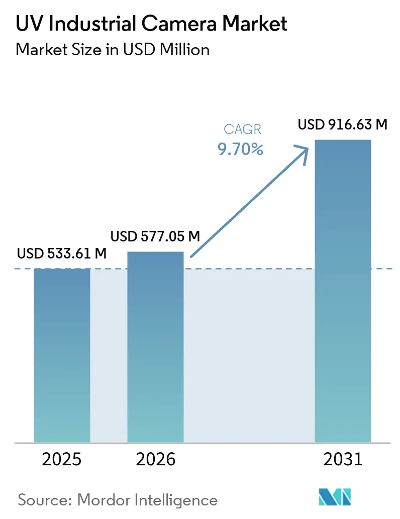
The UV industrial camera market size was valued at USD 533.61 million in 2025 and is estimated to expand from USD 577.05 million in 2026 to reach USD 916.63 million by 2031, at a CAGR of 9.70% during the forecast period (2026-2031). Investment in semiconductor fabrication, automated production lines, and renewable energy assets supports demand for UV-band inspection systems. UV imaging now supports inline quality control in recycling, electric-vehicle battery production, and high-voltage grid monitoring. This wider use reduces dependence on any 1 end-user group and creates demand across several manufacturing settings. Suppliers are improving sensor sensitivity, data transfer capacity, and integration support to address these use cases. The UV industrial camera market also faces constraints due to limited availability of optical components, export controls, and a shortage of specialists capable of aligning and calibrating UV systems.
Key Report Takeaways
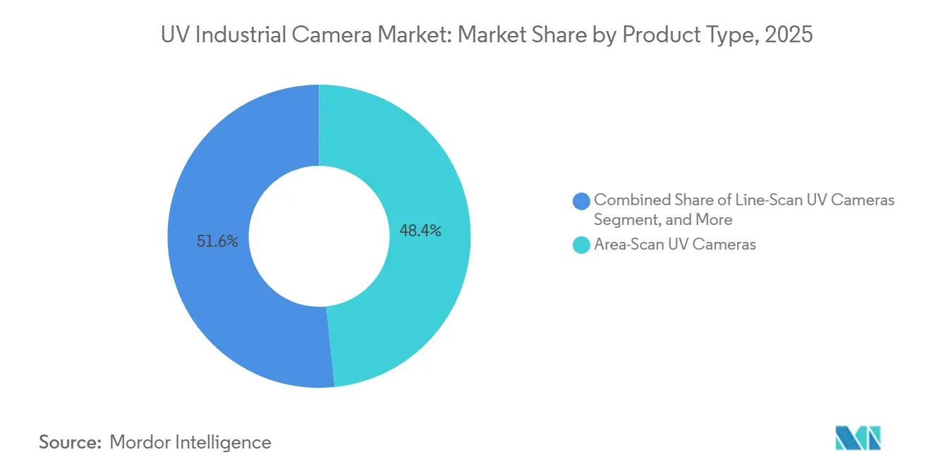
- By product type, area-scan UV cameras (non-intensified) held 48.37% of the UV industrial camera market share in 2025, while line-scan UV cameras are projected to expand at an 10.51% CAGR through 2031.
- By spectral range, UVA cameras held 44.27% revenue share in 2025, while UVC cameras are projected to expand at an 10.49% CAGR through 2031.
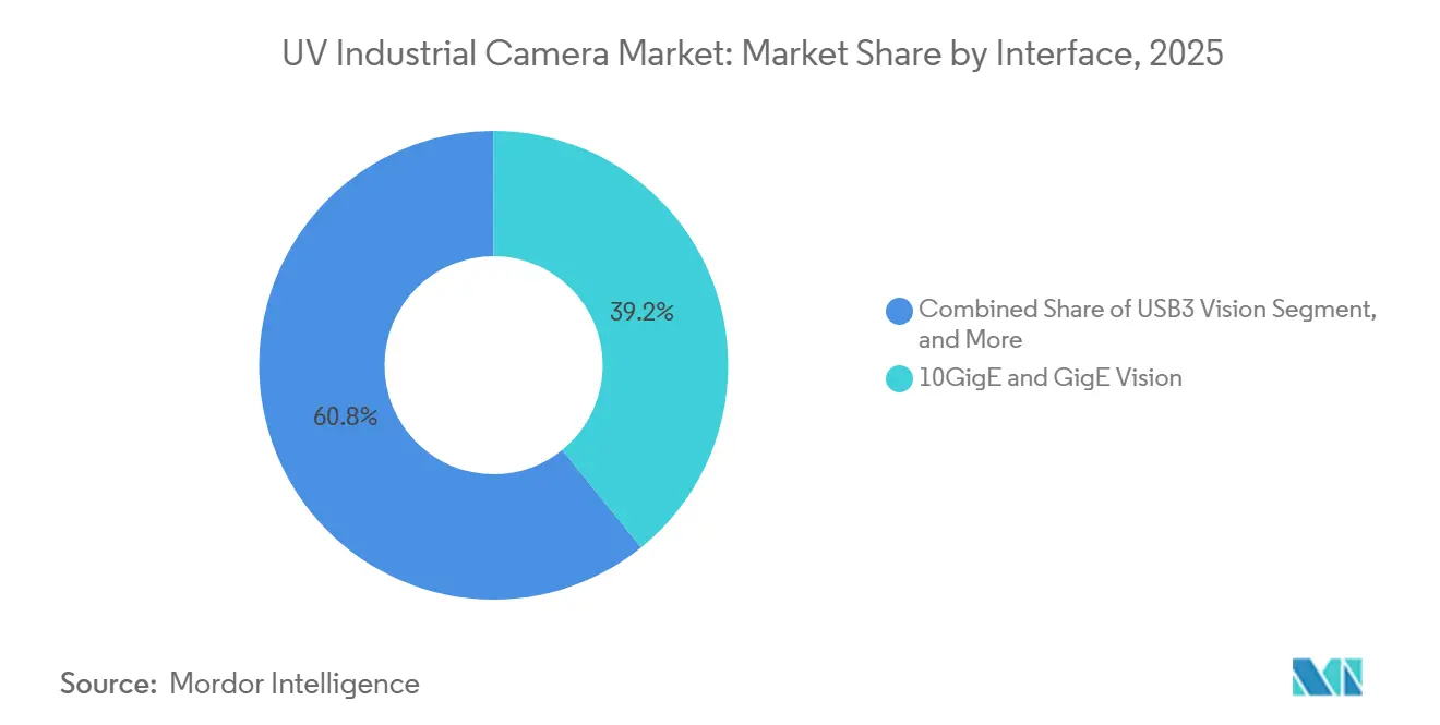
- By interface, 10GigE and GigE Vision held 39.18% revenue share in 2025, while CoaXPress is projected to expand at a 10.47% CAGR through 2031.
- By end-user industry, electronics and semiconductors accounted for 29.36% of revenue in 2025, while renewable energy is projected to expand at a 11.52% CAGR through 2031.
- By geography, Asia-Pacific held 45.82% of the UV industrial camera market share in 2025 and is projected to expand at a 10.68% CAGR through 2031.
Note: Market size and forecast figures in this report are generated using Mordor Intelligence’s proprietary estimation framework, updated with the latest available data and insights as of January 2026.
Global UV Industrial Camera Market Trends and Insights
Drivers Impact Analysis*
| Driver | (~) % Impact on CAGR Forecast | Geographic Relevance | Impact Timeline |
|---|---|---|---|
| Factory Automation and Industry 4.0 Adoption | +2.0% | Global, led by Asia-Pacific and Europe | Medium term (2-4 years) |
| Semiconductor and Advanced Electronics Inspection Intensity | +1.8% | Asia-Pacific core, with North America and Europe | Medium term (2-4 years) |
| Rising Demand for High-Speed, High-Resolution Inspection | +1.2% | Global | Short term (≤ 2 years) |
| Edge AI and Real-Time Defect Detection | +0.9% | Asia-Pacific and North America, with expansion to Europe | Short term (≤ 2 years) |
| UV-Based Sorting of Difficult Materials | +0.6% | Europe and North America | Medium term (2-4 years) |
| High-Speed UV Global-Shutter Sensors | +0.5% | Global | Short term (≤ 2 years) |
| Source: Mordor Intelligence | |||
Factory Automation and Industry 4.0 Adoption
Factory automation is expanding the use of UV cameras in automotive, electronics, and pharmaceutical assembly lines. UV imaging can detect surface contamination and micro-cracks that visible-light cameras may miss at conveyor speeds. This capability supports consistent inspection, which high throughput can otherwise compromise. A 2025 study reported detection accuracy above 95% for integrated machine-vision and programmable logic controller inspection scenarios. The UV industrial camera market benefits when factories add multiple inspection points within a single automated cell. System providers also benefit from offering camera hardware that integrates with established automation controls and communication networks.
Semiconductor and Advanced Electronics Inspection Intensity
Advanced semiconductor production requires inspection methods capable of detecting very small defects on patterned wafers. Sub-7 nm process nodes require wavelengths below 400 nm because visible light cannot resolve some feature-scale defects. Exosens stated in March 2026 that dark-field UV imaging can reveal edge defects and sub-pitch particles in dense patterned-wafer layouts. These requirements position UV cameras as equipment that protects yield rather than as an optional inspection addition. More inspection stages per process node can raise the number of cameras needed per wafer tool. SEMI S2, GigE Vision, and GenICam requirements can lengthen qualification cycles, but validated systems can face higher replacement barriers.
Rising Demand for High-Speed, High-Resolution Inspection
High-resolution UV inspection supports detailed imaging without reducing line speed. Sony’s IMX487 global-shutter CMOS sensor provides 8.13 megapixels at 193 frames per second across the 200-400 nm range. The sensor is used in UV camera designs from several machine-vision suppliers. CXP-12 provides 12.5 Gbps per link, which supports high-resolution image transmission with room for metadata. CoaXPress over Fiber can also place processing equipment away from demanding production environments. These capabilities support the UV industrial camera market, where wafer, web, and panel inspection require continuous image capture.
Edge AI and Real-Time Defect Detection
Edge-based AI reduces the time between image capture and process response. Inspection systems can classify anomalies at the production station instead of sending all images to a central server. A published SPIE paper described AI methods for inline nuisance filtering and whole-wafer pattern classification. This approach can reduce false-positive reviews and direct engineering attention to yield-limiting defects. In 2025, Fraunhofer IPMS and DIVE Imaging Systems demonstrated a cleanroom-qualified UV hyperspectral system that captured surface properties and contamination in 20 seconds per wafer.[1]“Optimierte Halbleiterprozesse,” Fraunhofer IPMS, ipms.fraunhofer.de. The UV industrial camera market can benefit from faster classification, which makes complex UV inspection easier to use on busy lines.
Restraints Impact Analysis*
| Restraint | (~) % Impact on CAGR Forecast | Geographic Relevance | Impact Timeline |
|---|---|---|---|
| High Initial System and Integration Cost | -1.5% | Global, more acute in South America, Africa, and the Middle East | Short term (≤ 2 years) |
| Shortage of UV Imaging and Machine-Vision Skills | -1.0% | Global, most pronounced in emerging markets | Medium term (2-4 years) |
| UV Optical Materials and Calibration Supply Bottlenecks | -0.7% | Global, originating in Japan, Germany, and the United States | Medium term (2-4 years) |
| Export Controls and Qualification Risk for Advanced UV Sensors | -0.5% | Cross-border, affecting Asia-Pacific and Middle East and Africa buyers | Long term (≥ 4 years) |
| Source: Mordor Intelligence | |||
High Initial System and Integration Cost
A complete UV inspection station requires a back-illuminated CMOS camera, UV-grade optics, interface hardware, frame grabbers, and edge processing equipment. These components make the initial system cost higher than for comparable visible-light systems. Balluff notes that UV and SWIR imaging require specialized optical and system choices for industrial applications.[2]“How UV and SWIR Are Revolutionizing Industrial Vision Systems,” Balluff, balluff.com. Complex multi-camera architectures may require a 6-12-week migration period. Production disruptions and engineering labor can add to hardware costs. The UV industrial camera market may therefore see slower adoption among cost-sensitive automotive suppliers, food processors, and recyclers until modular systems become more widely available.
Shortage of UV Imaging and Machine-Vision Engineering Skills
UV system design requires optical knowledge and machine-vision software skills. Engineers must understand UV absorption, fluorescence response, anti-reflection coatings, alignment, calibration, and image processing. This combination is scarce in markets that are beginning to adopt UV inspection. LUCID provides software environments that reduce low-level camera configuration work for users. However, dark-field alignment and calibration still require specialist work at the production site. The UV industrial camera market may see slower adoption when local integrators cannot specify the correct UV-grade components or train models on UV image data.
*Our forecasts treat driver/restraint impacts as directional, not additive. The impact forecasts reflect baseline growth, mix effects, and variable interactions.
Segment Analysis
By Product Type: Line-Scan Growth Outpaces a Stable Area-Scan Foundation
Area-scan UV cameras, non-intensified, accounted for 48.37% of the UV industrial camera market share in 2025. Their broad use reflects demand for semiconductor die inspection, solar-cell crack detection, and pharmaceutical serialization checks. These applications require precise imaging of stationary or step-indexed objects. Multiple suppliers offer IMX487-based designs, which gives buyers a wider choice of camera formats and prices. This availability supports deployment without redesigning the full optical path. The UV industrial camera market size for line-scan UV cameras is projected to expand at an 10.51% CAGR between 2026 and 2031. Continuous battery-electrode and large-format solar panel inspection favors single-pass imaging over repeated area-scan cycles.
MindVision’s MV-PXL90U is a 9K UV line-scan camera with a 529 kHz line rate, 256-plus-32 TDI stages, and water cooling for thermal stability. These specifications address the needs of original equipment manufacturers serving the high-throughput recycling and display-panel inspection markets. Intensified UV cameras retain a role where signal levels are extremely low. Their applications include nighttime corona detection, trace luminescence imaging, and mask inspection. Exosens’s i2Nocturn series covers 190-300 nm and uses double-MCP gain of 1,000,000 with a 1936×1216-pixel detector operating at 50 frames per second. UV-sensitive TDI cameras and modular sensor boards continue to serve research instruments and embedded vision systems.



By Spectral Range: UVC Band Gains Ground Beyond Traditional Disinfection Uses
UVA cameras, covering 320-400 nm, held 44.27% of the UV industrial camera market share in 2025. Back-illuminated IMX487 designs and common fluorescent tracers support their position. Pharmaceutical anti-counterfeiting, adhesive cure verification, and printed circuit board coating inspection are established uses of UVA. Recycling systems also use this band to distinguish PET, PVC, and polystyrene based on UV reflectance or fluorescence. The UV industrial camera market size for UVC cameras is projected to expand at an 10.49% CAGR from 2026 to 2031. Solar-blind UVC cameras can detect corona and arcing while blocking solar background during daytime utility inspections.
Photonfocus’s DUV camera began domestic sales in Japan in January 2026 through Aplolink. It supports imaging below 200 nm and covers the 193-nm ArF excimer laser band without fluorescence-conversion optics. MONOIST This capability supports lithography and laser micro-machining quality control. UVB cameras serve narrower uses in atmospheric gas monitoring, medical dermatology, and fluorescence spectroscopy. Broad-spectrum and multispectral UV cameras combine UV, visible, and near-infrared channels for stations that need more than 1 inspection band. Tucsen Photonics’s Libra UV covers 200-1000 nm and reports up to 48% quantum efficiency at 365 nm.
By Interface: CoaXPress Is the High-Bandwidth Choice for New Designs
10GigE and GigE Vision held 39.18% of the UV industrial camera market share in 2025. The installed base of Ethernet machine-vision equipment supports this position. GigE Vision and GenICam also provide a familiar integration route for equipment builders using visible-light and UV cameras. LUCID Vision Labs’ Atlas10 UV combines 10GigE Power over Ethernet connectivity with the IMX487 sensor. This design enables full-resolution image transmission without a proprietary frame grabber. The UV industrial camera market size for CoaXPress is projected to expand at a 10.47% CAGR from 2026 to 2031.
CXP-12 specifications provide 12.5 Gbps per link for UV line-scan and high-frame-rate area-scan systems. The interface also supports deterministic triggering for synchronized multi-camera cells. GenICam compliance is required for CoaXPress products, and semiconductor equipment buyers may favor its Power-over-CoaXPress capability in cleanrooms. USB3 Vision remains useful for cost-sensitive research and life-science systems that do not require Power over Ethernet. Camera Link and other interfaces are becoming less relevant as CXP-12 replaces earlier high-bandwidth configurations. CoaXPress v3.0 was under development in early 2026, with a planned 25 Gbps per-link capability and native CoaXPress-over-Fiber support.
By End-User Industry: Renewable Energy Adds a High-Volume Opportunity Beyond Semiconductor
Electronics and semiconductors accounted for 29.36% of the UV industrial camera market share in 2025. Dark-field wafer inspection, mask-defect detection, and packaging verification support this leading position. Each advanced process node can add inspection stages and require smaller defect thresholds. As a result, UV camera use per wafer can rise faster than wafer output. The UV industrial camera market size for renewable energy is projected to expand at a 11.52% CAGR from 2026 to 2031. Demand comes from photovoltaic encapsulant checks, battery electrode surface inspections, and corona monitoring at solar farms and electric vehicle charging infrastructure.
Allied Vision identifies line-scan cameras as relevant to solar and battery inspection applications. Automotive and electric-vehicle applications include battery electrodes, sealants, adhesive bonds, and glass-ceramic parts for power electronics. Aerospace and defense users apply intensified UV cameras to fluorescence penetrant inspections of composite and metallic components. Pharmaceutical, food, and consumer packaging systems use UV imaging for authenticity checks and surface contamination detection. Utilities, rail, and infrastructure operators use solar-blind cameras to identify corona and arcing on transmission assets. Ofil describes the use of its UV EYE family in continuous substation, robotic, vehicle-mounted, and rail inspections.
Geography Analysis
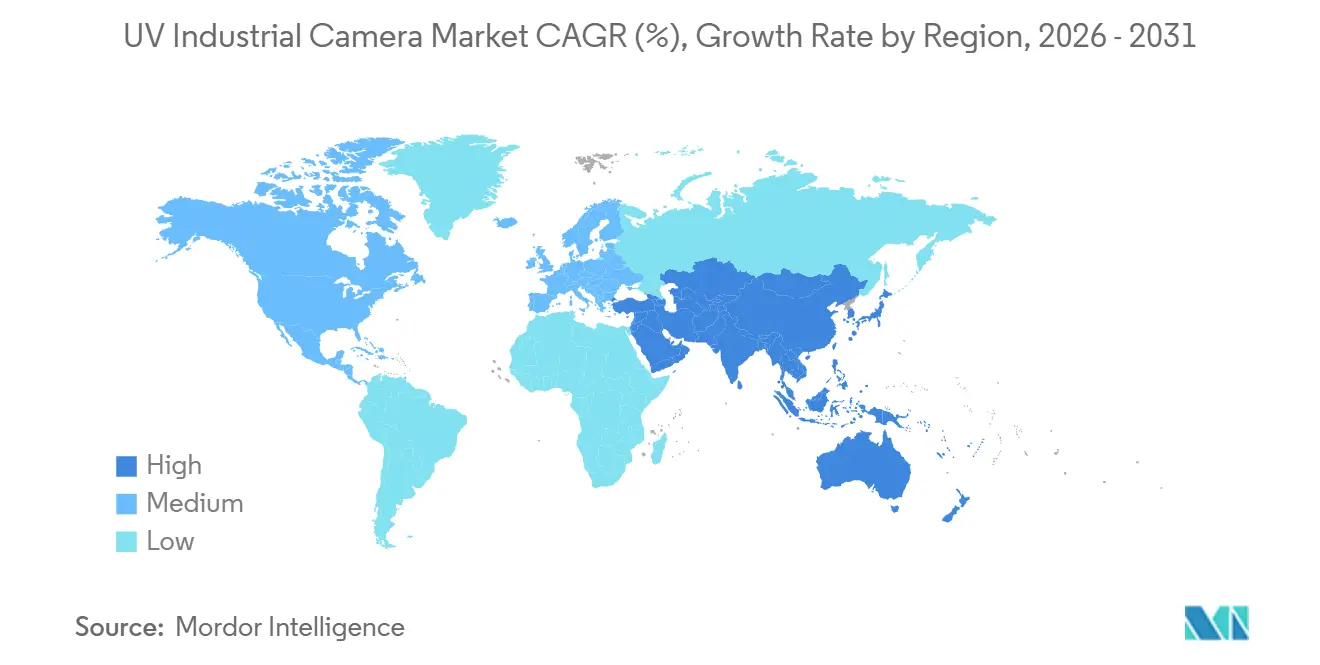
Asia-Pacific held 45.82% of the UV industrial camera market share in 2025 and is projected to expand at a 10.68% CAGR through 2031. China, Japan, South Korea, and Taiwan are key demand centers because they host semiconductor fabrication, photovoltaic manufacturing, and consumer-electronics assembly. These industries need UV inspection for high-throughput production and quality control. China is developing domestic UV camera supply chains as export restrictions increase the need for local technical capacity. Tucsen Photonics has expanded its UV offering across semiconductor inspection applications.[3]“Choosing the Right UV Camera for Semiconductor Inspection,” Tucsen Photonics, tucsen.com.
Japan remains both a producer and a buyer of UV imaging technology. Hamamatsu Photonics and ARTRAY support the country’s position in UV component development and industrial imaging. Konica Minolta announced a March 2026 strategy for VIS, UV, and DUV optical components used in semiconductor inspection tools. The company set a 2030 revenue target of JPY 150 billion (USD 1.01 billion) for this business. India and Southeast Asia provide further demand as new semiconductor, lithium-ion battery, and solar facilities are built. The UV industrial camera market has scope to supply these facilities as they add inline inspection equipment.
North America and Europe remain important because of semiconductor investment and established machine-vision expertise. The United States supports expanding domestic semiconductor manufacturing, while Germany hosts Allied Vision Technologies and several industrial vision integrators. Exosens SE in France supplies intensified UV systems for semiconductor and defense buyers. The United Kingdom and France also support research and demand for life-science imaging. Italy’s pharmaceutical and food packaging sectors use UV systems for serialization and authenticity checks. South America, the Middle East, and Africa are smaller markets where solar projects, mining inspection, recycling, automotive production, and electronics manufacturing can create incremental demand.

Competitive Landscape
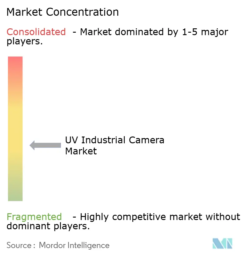
The UV industrial camera market is moderately fragmented, with 20 named vendors and many smaller original equipment manufacturers. No single supplier has a dominant position. Competition centers on sensitivity, interface bandwidth, price, and support for application-specific integration. Several suppliers adopted Sony’s IMX487 sensor within 12 months of its release, shifting differentiation toward software and camera format. Sony positions its UV image-sensor technology for industrial applications that require UV sensitivity. This structure gives buyers a choice of products, while suppliers must show clear value in performance and deployment support.
Emergent Vision Technologies offers the IMX487 UV sensor on 10GigE, 25GigE, and 100GigE platforms. This approach allows users to select a bandwidth tier without changing the optical design. Exosens focuses on intensified cameras for dark-field semiconductor inspection, where standard CMOS substitution may not provide comparable photon sensitivity. Its March 2026 technical publication described how i2Nocturn and iNocturn cameras detect particle contamination and edge defects in dense-patterned wafers.[4]“Wafer Inspection at Advanced Nodes,” Exosens, exosens.com. Allied Vision uses its ALVIUM System-on-Chip architecture to address pipeline latency and power consumption.
The UV industrial camera industry has opportunities in compact, rugged cameras for field utility inspection. Systems with IP67-class housings and Power over Ethernet remain limited in UV optical quality. AI-integrated cameras that perform inference at the sensor also represent an area of product development. Chinese suppliers are entering sub-200 nm DUV imaging, which can broaden competitive pressure in advanced inspection uses. Photonfocus’s January 2026 DUV camera launch in Japan showed direct imaging capabilities for 193 nm and 248 nm excimer laser beams. These product strategies place sensor performance, communication speed, and practical integration at the center of competition among suppliers.
UV Industrial Camera Industry Leaders
Allied Vision Technologies GmbH
Basler AG
Teledyne Technologies Incorporated
ARTRAY Co., Ltd.
Photonfocus AG
- *Disclaimer: Major Players sorted in no particular order

Recent Industry Developments
- August 2026: LUCID Vision Labs announced a new cohort of GigE Vision cameras, including 8K line-scan, NIR low-light, STARVIS 2, and RGB-D 3D models, ahead of VISION 2026 in Stuttgart. The announcement signaled continued multispectral portfolio expansion that shared platform architecture with the company’s existing Atlas10 UV lineup.
- May 2026: Teledyne DALSA introduced Kaleido, a SWIR hyperspectral camera for industrial sorting applications in recycling, pharmaceuticals, and waste management. It featured a 10GigE interface compliant with GigE Vision and GenICam standards and addressed applications adjacent to UV-based sorting deployments.
- March 2026: Basler AG and Orbbec announced a technology partnership to develop industrial 3D vision solutions. The Basler Stereo mini camera was presented at LogiMAT 2026 and expanded Basler’s portfolio into AMR and AGV automation markets alongside its UV camera lines.
- March 2026: Exosens published a technical article on UV dark-field wafer inspection at advanced nodes. It detailed how its i2Nocturn and iNocturn intensified UV cameras revealed sub-pitch particle contamination and edge defects in dense patterned-wafer layouts that standard bright-field inspection missed.


Global UV Industrial Camera Market Report Scope
The UV Industrial Camera Market comprises specialized imaging cameras designed to detect, capture, and analyze ultraviolet (UV) radiation or UV-reflective and UV-emissive characteristics of objects, materials, processes, and environments for industrial inspection, monitoring, measurement, and quality-control applications. UV industrial cameras convert ultraviolet wavelengths into digital images and are used where conventional visible-light imaging cannot adequately identify defects, contamination, electrical discharges, material characteristics, or other process conditions.
The UV Industrial Camera Report is Segmented by Product Type (Area-Scan UV Cameras, Line-Scan UV Cameras, Intensified UV Cameras, and Other Product Types), Spectral Range (UVA Cameras, UVB Cameras, UVC Cameras, and Broad-Spectrum and Multispectral UV Cameras), Interface (CoaXPress, 10GigE and GigE Vision, USB3 Vision, and Camera Link and Other Interfaces), End-User Industry (Electronics and Semiconductor, Automotive and Electric Vehicle, Renewable Energy, Recycling and Waste Management, Aerospace and Defense, Pharmaceuticals, Food, and Consumer Packaging, Utilities, Rail, and Infrastructure, Research and Life Sciences, and Other End-User Industries), and Geography (North America, South America, Europe, Asia-Pacific, Middle East, and Africa). The Market Forecasts are Provided in Terms of Value (USD).
| Area-Scan UV Cameras |
| Line-Scan UV Cameras |
| Intensified UV Cameras |
| Other Product Types |
| UVA Cameras |
| UVB Cameras |
| UVC Cameras |
| Broad-Spectrum and Multispectral UV Cameras |
| CoaXPress |
| 10GigE and GigE Vision |
| USB3 Vision |
| Camera Link and Other Interfaces |
| Electronics and Semiconductor |
| Automotive and Electric Vehicle |
| Renewable Energy |
| Recycling and Waste Management |
| Aerospace and Defense |
| Pharmaceuticals, Food, and Consumer Packaging |
| Utilities, Rail, and Infrastructure |
| Research and Life Sciences |
| Other End-User Industries |
| North America | United States |
| Canada | |
| Mexico | |
| South America | Brazil |
| Argentina | |
| Rest of South America | |
| Europe | Germany |
| United Kingdom | |
| France | |
| Italy | |
| Rest of Europe | |
| Asia-Pacific | China |
| Japan | |
| South Korea | |
| Taiwan | |
| India | |
| Rest of Asia-Pacific | |
| Middle East | Turkey |
| Saudi Arabia | |
| United Arab Emirates | |
| Rest of Middle East | |
| Africa | South Africa |
| Egypt | |
| Rest of Africa |
| By Product Type | Area-Scan UV Cameras | |
| Line-Scan UV Cameras | ||
| Intensified UV Cameras | ||
| Other Product Types | ||
| By Spectral Range | UVA Cameras | |
| UVB Cameras | ||
| UVC Cameras | ||
| Broad-Spectrum and Multispectral UV Cameras | ||
| By Interface | CoaXPress | |
| 10GigE and GigE Vision | ||
| USB3 Vision | ||
| Camera Link and Other Interfaces | ||
| By End-User Industry | Electronics and Semiconductor | |
| Automotive and Electric Vehicle | ||
| Renewable Energy | ||
| Recycling and Waste Management | ||
| Aerospace and Defense | ||
| Pharmaceuticals, Food, and Consumer Packaging | ||
| Utilities, Rail, and Infrastructure | ||
| Research and Life Sciences | ||
| Other End-User Industries | ||
| By Geography | North America | United States |
| Canada | ||
| Mexico | ||
| South America | Brazil | |
| Argentina | ||
| Rest of South America | ||
| Europe | Germany | |
| United Kingdom | ||
| France | ||
| Italy | ||
| Rest of Europe | ||
| Asia-Pacific | China | |
| Japan | ||
| South Korea | ||
| Taiwan | ||
| India | ||
| Rest of Asia-Pacific | ||
| Middle East | Turkey | |
| Saudi Arabia | ||
| United Arab Emirates | ||
| Rest of Middle East | ||
| Africa | South Africa | |
| Egypt | ||
| Rest of Africa | ||


Key Questions Answered in the Report
What is the size of the UV industrial camera market?
The market was valued at USD 533.61 million in 2025 and is estimated at USD 577.05 million in 2026. It is forecast to reach USD 916.63 million by 2031 at a 9.70% CAGR.
Which UV industrial camera product type leads demand?
Area-scan UV cameras, non-intensified, led product demand with 48.37% share in 2025. They support detailed inspection of semiconductor, solar, and pharmaceutical products.
Which UV camera spectral range is expanding fastest?
UVC cameras are projected to expand at an 10.49% CAGR through 2031. Utility operators use solar-blind UVC cameras for daytime corona and arcing detection.
Why are semiconductor manufacturers using UV cameras?
UV systems can identify wafer defects that visible-light cameras may not resolve at advanced process nodes. They support dark-field inspection, mask checks, and packaging verification.
Which geographic area has the strongest demand for UV industrial cameras?
Asia-Pacific held 45.82% share in 2025 and is projected to expand at a 10.68% CAGR through 2031. Semiconductor, photovoltaic, and consumer-electronics production support demand.
What limits wider use of UV inspection systems?
High system cost and limited specialist skills can delay deployment. UV optical materials, calibration needs, and export-control requirements can add complexity for buyers and system integrators.
Page last updated on:


 Your data is secure and never sold or shared.


