
Size and Share of United States Solder Materials Market In Semiconductor Industry
Market Overview
| Study Period | 2021 - 2032 |
|---|---|
| Forecast Data Period | 2027 - 2032 |
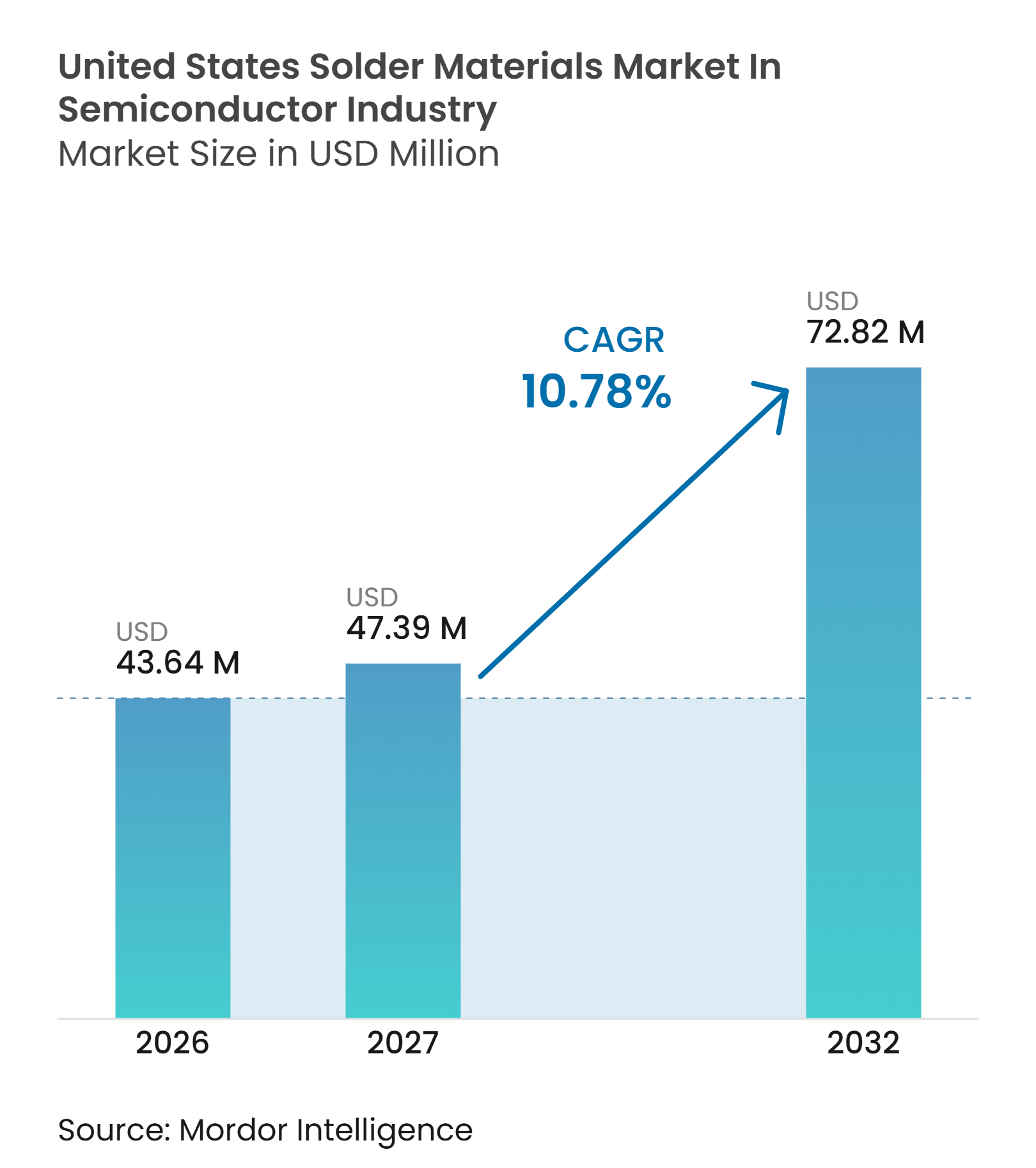
| Base Year Market Size (2026) | USD 43.64 Million |
| Market Size (2027) | USD 47.39 Million |
| Market Size (2032) | USD 72.82 Million |
| Growth Rate (2027 - 2032) | 10.78 % |
| Market Concentration | Medium |
Major Players *Disclaimer: Major Players sorted in no particular order Image © Mordor Intelligence. Reuse requires attribution under CC BY 4.0. | |
Analysis of United States Solder Materials Market In Semiconductor Industry by Mordor Intelligence
The United States solder materials market in semiconductor industry was valued at USD 43.64 million in 2026 and is estimated to reach USD 72.82 million by 2032, at a CAGR of 10.78% during 2027-2032. The United States solder materials market is being shaped by new domestic advanced packaging capacity, which raises the need for qualified solder pastes, balls, preforms, and fluxes. Demand for AI processors and high-bandwidth memory is increasing the technical importance of package interconnects, particularly in wafer-level and multi-die designs. Material suppliers are competing through formulations that address fine pitches, thermal reliability, and lead-free requirements rather than through price alone. Public packaging programs and planned facilities in Arizona are likely to reinforce demand for qualified local supply chains. Metals price volatility and the time needed to qualify new alloys remain important limits on purchasing decisions and production planning.
Key Report Takeaways
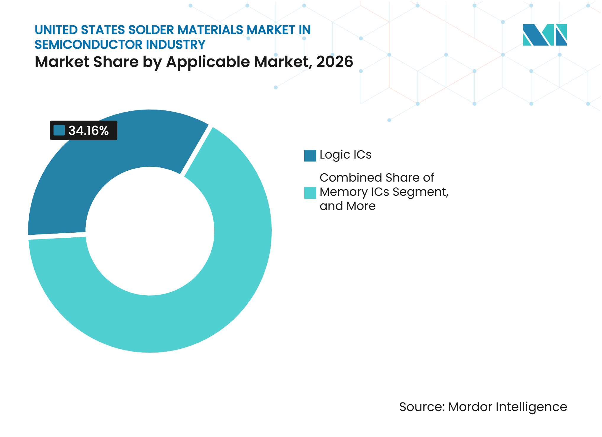
- By applicable market, logic ICs held 34.16% of the United States solder materials market in semiconductor industry share in 2026.
- By product form, solder paste held 36.28% of the United States solder materials market in semiconductor industry and is projected to expand at an 11.34% CAGR through 2032.
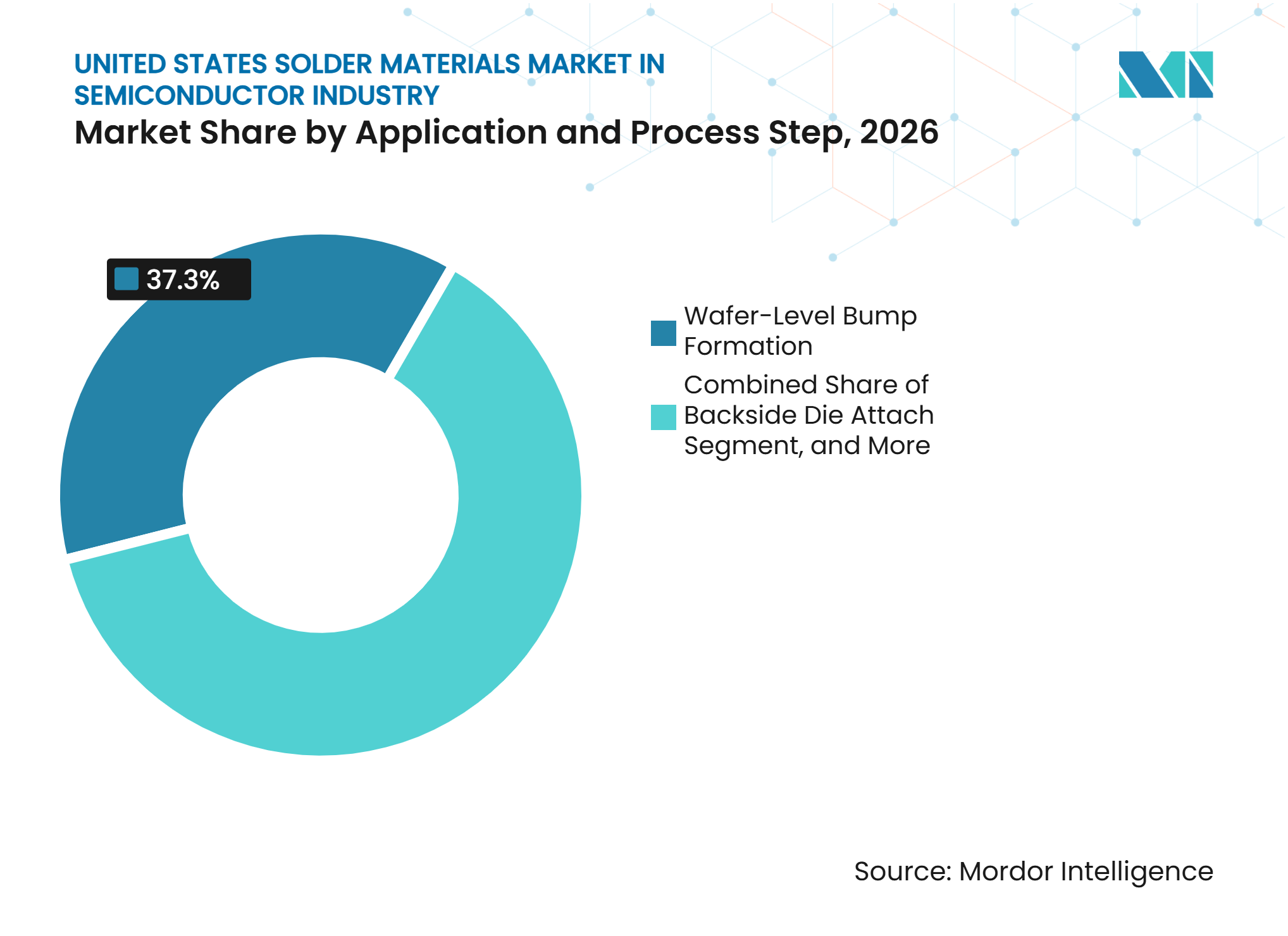
- By application and process step, wafer-level bump formation accounted for 39.14% of the United States solder materials market in semiconductor industry share in 2026, and is projected to expand a 12.48% CAGR through 2032.
Note: Market numbers in this report are based on Mordor Intelligence's proprietary estimation framework, which combines nine months of actuals with Q4 projections for base year 2026.
Market Trends and Insights
Drivers Impact Analysis of United States Solder Materials Market of United States Solder Materials Market In Semiconductor Industry*
| Driver | (~) % Impact on CAGR Forecast | Geographic Relevance | Impact Timeline |
|---|---|---|---|
| Expansion of United States Semiconductor Packaging Capacity | +3.2% | National, with early gains concentrated in Arizona, New Mexico, and Oregon | Short term (≤ 2 years) |
| Advanced Packaging Adoption in AI and High-Performance Computing | +2.8% | National, with primary demand in Arizona fab clusters and Pacific Northwest R&D centers | Medium term (2-4 years) |
| Lead-Free Conversion and Environmental Compliance | +1.9% | National, with urgency in California, New York, and states mirroring EU RoHS frameworks | Medium term (2-4 years) |
| Rising Semiconductor Content in Automotive Electronics | +1.5% | National, with early adoption in Michigan, Ohio, and Texas | Medium term (2-4 years) |
| Finer-Pitch Interconnect Requirements in Miniaturized Devices | +1.2% | National, with intensity in Arizona, California, and Oregon fab clusters | Long term (≥ 4 years) |
| Domestic Demand for High-Reliability Specialty Solder Materials | +0.9% | National, with defense and aerospace hubs in Virginia, Connecticut, and California | Long term (≥ 4 years) |
| Source: Mordor Intelligence | |||
Expansion of United States Semiconductor Packaging Capacity
The expansion of domestic packaging capacity is the leading demand driver for the United States solder materials market in semiconductor industry. The U.S. Department of Commerce finalized USD 1.4 billion in National Advanced Packaging Manufacturing Program awards in January 2025, including USD 1.1 billion for Natcast’s Advanced Packaging Piloting Facility in Tempe, Arizona.[1] The program adds a domestic platform for wafer bumping, flip-chip assembly, and related materials work. Each new packaging line requires a qualification cycle for an alloy and process combination, which supports demand for suppliers already able to meet those requirements. TSMC announced a USD 165 billion United States investment plan in March 2025 that includes 3 new fabrication plants and 2 advanced packaging facilities in Arizona.[2] The planned facilities strengthen the case for domestic availability of qualified solder materials at scale.
Advanced Packaging Adoption in AI and High-Performance Computing
AI and high-performance computing are shifting packaging from a supporting assembly activity to a central route for improving chip performance. The United States solder materials market benefits because multi-die packages use dense solder interconnects in micro-bumps, flip-chip assembly, and wafer-level processes. IEEE’s 2026 Heterogeneous Integration Roadmap identifies advanced manufacturing and multi-chip integration as core areas of packaging development. These systems require close control of particle distribution, wetting behavior, and paste deposition. Larger AI packages can use more interconnects even when individual bumps become smaller. This pattern supports demand for high-specification products that meet process and reliability requirements.
Lead-Free Conversion and Environmental Compliance
Lead-free conversion is increasing material development and qualification work across the United States solder materials market. European RoHS rules continue to affect products sold into regulated end markets, while state-level requirements can reinforce similar procurement expectations. Material suppliers are responding with lead-free alternatives for applications that previously relied on high-melting-temperature alloys. Senju Metal Industry introduced its NFTLP bonding material for power semiconductor die attach in 2025, with stated heat resistance above 700°C after joining at 250°C and thermal conductivity above 35 W/m·K.[3] Such products can reduce reliance on lead-based materials in demanding applications. The transition still requires lengthy testing for each device class, so established suppliers with proven data have an advantage.
Rising Semiconductor Content in Automotive Electronics
Automotive electronics are increasing the need for solder materials that manage high temperatures, high current loads, and repeated thermal cycling. EV inverters, battery management systems, and silicon carbide gate drivers place greater demands on die attach and interconnect reliability. The United States solder materials market therefore has room for alloys and pastes tailored to high-reliability automotive assembly. KOKI launched SB6NX58-G850 in June 2025 for harsh automotive and industrial conditions, with a solid-solution-strengthened alloy and low-void performance. Suppliers are pursuing different routes for the same need, including silver sintering for premium programs and low-silver or tin-antimony formulations for cost-sensitive applications. This creates separate product positions within automotive electronics rather than a single technical standard.
Restraints Impact Analysis of United States Solder Materials Market of United States Solder Materials Market In Semiconductor Industry*
| Restraint | (~) % Impact on CAGR Forecast | Geographic Relevance | Impact Timeline |
|---|---|---|---|
| Tin, Silver, Copper, and Lead Price Volatility | -1.4% | Global, with direct cost pass-through to United States semiconductor assembly operations | Short term (≤ 2 years) |
| Higher Reflow Temperatures and Qualification Costs for Lead-Free Alloys | -0.9% | National, with greatest impact in advanced-node packaging and high-reliability assembly | Medium term (2-4 years) |
| Extended Reliability Qualification for Advanced Packaging Materials | -0.6% | National, including aerospace, defense, and automotive assembly operations | Long term (≥ 4 years) |
| Limited Domestic Capacity for Certain Ultrafine Powders and Micro-Spheres | -0.5% | National, with the largest gap in fine-pitch and sub-50 µm solder powder production | Long term (≥ 4 years) |
| Source: Mordor Intelligence | |||
Tin, Silver, Copper, and Lead Price Volatility
Metal price volatility is a near-term constraint for the United States solder materials market, as raw materials account for a significant share of alloy costs. Reuters reported that tin reached a record high following a sharp increase in an illiquid market. As tin is the primary component of SAC alloys, price fluctuations can rapidly affect the costs of solder paste, balls, and preforms. Copper also reached a record high, according to London Metal Exchange data cited by Fastmarkets. Silver prices add further pressure because the metal contributes significantly to the cost of SAC alloys despite its lower proportion by weight. Suppliers and customers may consider low-silver alloys; however, this transition can require process validation and reliability testing.
Higher Reflow Temperatures and Qualification Costs for Lead-Free Alloys
Lead-free alloys can require higher reflow temperatures than eutectic tin-lead systems, which increases thermal exposure during assembly. This is particularly relevant for large AI processor packages with complex warpage behavior. The United States solder materials market must also account for qualification cycles that can last 12-24 months for a new alloy in automotive, aerospace, and high-reliability semiconductor applications. Indium Corporation reported in April 2026 that its collaborative work on solder alloy reliability examined bismuth-free, indium-containing low-temperature solutions for heterogeneous integration. Lower-temperature options can help manage package warpage, but they do not remove the need for extensive validation. Smaller outsourced semiconductor assembly and test providers may face more difficulty absorbing the technical and financial cost of those programs.
*Our forecasts treat driver/restraint impacts as directional, not additive. The impact forecasts reflect baseline growth, mix effects, and variable interactions.
United States Solder Materials Market In Semiconductor Industry Segment Analysis
By Applicable Market:
Logic ICs Drive Advanced Packaging IntensityLogic ICs accounted for a 34.16% share of the applicable market in 2026. This position reflects demand from AI accelerators, graphics processing units, and next-generation CPUs that use dense flip-chip micro-bump arrays. These devices support 2.5D and 3D integration formats where material specifications are closely tied to package yield. The United States solder materials market in semiconductor industry size for logic IC applications is supported by strict requirements for solder composition, powder size, and interconnect uniformity. Compound semiconductors and power devices form an important secondary opportunity because silicon carbide and gallium nitride systems require strong thermal performance.
Memory ICs also support demand through high-bandwidth memory stacks, where solder micro-bumps join successive DRAM dies. These packages require fine-powder paste grades that can form consistent features at tight pitches. Analog ICs, sensors, MEMS, and RF devices are lower-volume applications, but they require specialized flux systems and, in some cases, fluxless soldering. Optical and photonic devices add another specialized requirement as domestic photonic packaging activity develops. Pennsylvania announced federal support of up to USD 172 million for 2 technology companies in 2025, including funding connected to Infinera’s Bethlehem facility.


By Product Form:
Solder Paste Leads an Innovation-Intensive PortfolioSolder paste is projected to expand at an 11.34% CAGR through 2032, making it the fastest-growing product form in the United States solder materials market in semiconductor industry. Fine-pitch stencil printing supports its demand because it can address throughput and cost requirements in advanced assembly. IEEE research presented at EPTC 2025 described a wafer-level micro-bumping solution using Type 6 powder and an optimized flux system that achieved consistent bump formation at 140 µm pitch. SHENMAO introduced PF606-P279L in November 2025 for ultra-fine-pitch printing and 60 µm stencil apertures in mini-LED and system-in-package production.
Solder preforms carry high unit value because they are precision-stamped for die attach, lid sealing, and hermetic packaging. Their role is important in defense electronics and advanced automotive systems where repeatable geometry and thermal performance are necessary. Solder wire and standalone fluxes continue to serve wave soldering, rework, and selected assembly operations. Solder powder is also sold as an input for paste production and plating processes. Formic-acid-compatible fluxless systems represent a developing product category for applications where residue control matters. KOKI introduced the E14 Series in 2025 for formic acid reduction reflow furnaces and power device soldering.
By Application and Process Step:
Wafer-Level Processes Define Value ConcentrationWafer-level bump formation held a 39.14% share of the applicable market in 2026. This application uses micro-bump and pillar-bumping processes for flip-chip, chip-on-wafer-on-substrate, and 3D IC assembly. The United States solder materials market in semiconductor industry size for wafer-level bump formation is shaped by the premium material intensity of these processes. Type 4-Type 7 solder powders are used in controlled paste formulations where particle distribution and wetting behavior affect bump uniformity. IEEE’s roadmap notes that advanced manufacturing methods are central to multi-chip integration, which supports continued focus on materials control at this step.
Copper-to-copper hybrid bonding may reduce solder use at the finest pitches, creating a structural risk for part of the wafer-level solder demand base. It may also create adjacent opportunities for materials needed in nearby assembly and interface steps. Die-to-substrate interconnection through conventional flip-chip remains a major application and often uses controlled-collapse interconnects above 100 µm pitch. Package-to-board interconnection has the highest solder ball unit count because advanced packages are generally attached to printed circuit boards through BGA or related formats. Backside die attach uses solder preforms or sinter pastes in power devices and high-power processors that need thermal control.
Geography Analysis
Arizona Semiconductor Manufacturing Cluster
Arizona is expected to remain a major demand centre for the United States solder materials market in semiconductor industry, supported by the concentration of new semiconductor fabrication and advanced packaging investments. TSMC's expansion in the United States includes plans for advanced packaging facilities in Arizona, creating opportunities for local procurement of solder balls, micro-bump pastes, and preforms used in advanced package assembly. The Natcast Advanced Packaging Piloting Facility in Tempe provides an additional public-sector platform for materials testing, process development, and packaging innovation. Together, these public and private investments strengthen Arizona's importance as a centre for solder materials qualification, supplier engagement, and commercial production ramp-up.
Pacific Coast and Oregon Advanced Technology Hub
California and Oregon contribute to the United States solder materials market in semiconductor industry through semiconductor product design, materials research, fabrication, and packaging qualification activities. California hosts major fabless semiconductor companies whose artificial intelligence and high-performance computing architectures influence advanced packaging requirements and material specifications. The U.S. Department of Commerce has also supported Applied Materials' silicon-core substrate development activities in Santa Clara, strengthening the regional advanced packaging ecosystem. As substrate architectures and interconnection technologies evolve, solder materials suppliers must demonstrate compatibility with new interface materials and packaging processes. California's environmental and lead-free material requirements further reinforce the importance of verified product reliability, regulatory compliance, and environmental documentation.
Diversifying Domestic Fab Base
Texas, Ohio, New York, Idaho, New Mexico, Pennsylvania, and other states broaden the geographic footprint of the United States solder materials market through semiconductor fabrication, specialized packaging, and materials development activities. New York combines GlobalFoundries' manufacturing operations in Malta with Indium Corporation's headquarters in Clinton, providing an established ecosystem for semiconductor manufacturing and advanced solder alloy development. Pennsylvania's federally supported photonics initiatives create additional opportunities for precision soldering and thermal management materials used in specialized packaging applications. Meanwhile, semiconductor manufacturing investments in New Mexico, Texas, and Ohio are expanding the domestic fabrication base and associated materials requirements. This geographically distributed ecosystem favors suppliers capable of providing consistent technical support, reliable material availability, and sustained customer qualification assistance across multiple manufacturing locations.
Competitive Landscape
Market Concentration
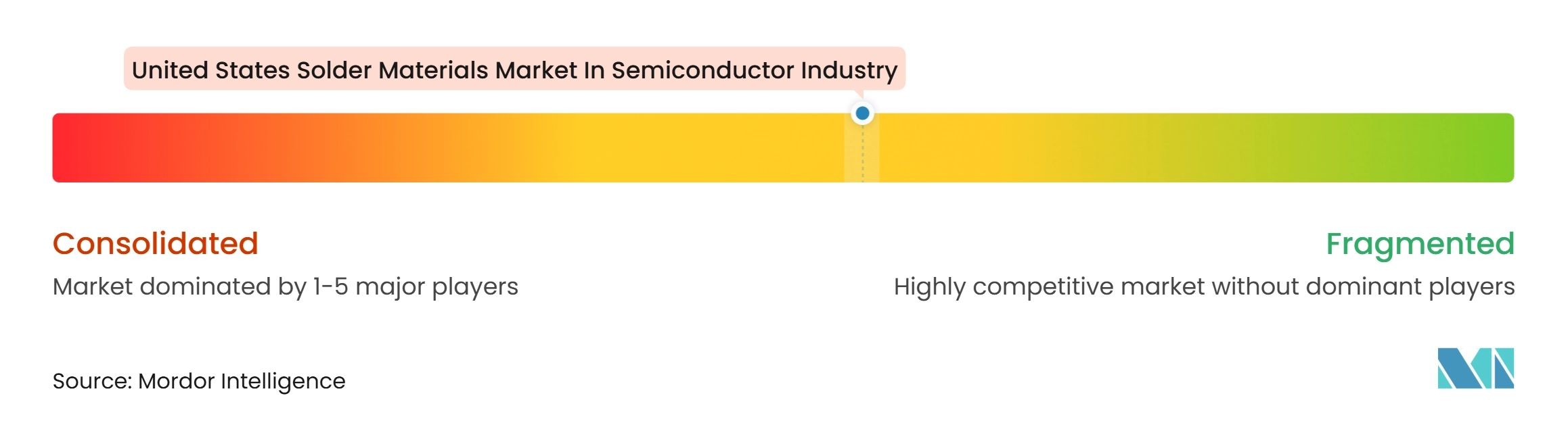
The United States solder materials market has moderate concentration at the premium alloy tier. Indium Corporation, MacDermid Alpha Electronics Solutions, and Henkel hold established positions through proprietary formulations and long-term qualification relationships with integrated device manufacturers and outsourced semiconductor assembly and test providers. Competition centers on products that move beyond standard SAC305, including bismuth-free, indium-containing, copper-sintering, and silver-sintering solutions. In February 2025, MacDermid Alpha, Heraeus Electronics, and Henkel announced the conclusion of German patent proceedings against Senju involving Innolot alloy technology. The outcome highlighted the importance of intellectual property in advanced lead-free alloy markets. RoHS-related compliance factors and state-level environmental expectations also shape purchasing criteria.
Henkel is seeking a position in high-power semiconductor packaging through copper-sintering materials, which target thermal management needs in silicon carbide applications. The company has stated that its material can deliver thermal conductivity above 300 W/m·K under 200-250°C and 10-15 MPa conditions. Indium Corporation has focused on low-temperature, bismuth-free material development for complex heterogeneous packages. Its September 2026 presentation described a DFLT solder with drop-shock resistance above bismuth-tin-silver alternatives and performance comparable to SAC305 at lower peak reflow temperatures. MacDermid Alpha has pursued power module reliability through BondPad technology for silicon carbide topside attachment. These examples show that suppliers are competing by addressing specific package and reliability challenges.
A further opportunity lies in domestic production of ultrafine Type 7 and Type 8 solder powders with particle diameters of 2-11 µm. IEEE’s Hardware and Infrastructure Roadmap identifies supply chain issues as a significant part of the advanced electronics landscape. Smaller suppliers such as AIM Solder and FCT Assembly serve broader assembly needs, while Japanese specialists retain North American relationships through qualified products and distribution networks. Senju’s NFTLP platform targets lead-free power semiconductor die attach, and KOKI has expanded low-silver paste options to manage material cost pressure. Market access depends on product performance, process support, and the ability to complete long customer validation cycles.
Leaders of United States Solder Materials Market In Semiconductor Industry
-
Indium Corporation
-
MacDermid Alpha Electronics Solutions
-
Kester, LLC
-
Henkel AG & Co. KGaA
-
Senju Metal Industry Co., Ltd.
- *Disclaimer: Major Players sorted in no particular order
United States Solder Materials Market In Semiconductor Industry Companies Covered in this Report
- Indium Corporation
- MacDermid Alpha Electronics Solutions
- Kester, LLC
- Henkel AG & Co. KGaA
- Senju Metal Industry Co., Ltd.
- AIM Solder
- Nihon Superior Co., Ltd.
- Heraeus Electronics
- KOKI Company Ltd.
- Qualitek International, Inc.
- SHENMAO Technology Inc.
- FCT Assembly, LLC
- Tamura Corporation
- Balver Zinn GmbH
- Stannol GmbH & Co. KG
- MG Chemicals Ltd.
- FlipChip International, LLC
- Micross Components, Inc.
- PacTech USA, Inc.
- QP Technologies, Inc.
Recent Industry Developments in United States Solder Materials Market In Semiconductor Industry
- November 2026: MacDermid Alpha Electronics Solutions unveiled BondPad technology at electronica 2026 in Munich, an Argomax film-laminated copper-foil solution for SiC power module topside attach achieving more than 75,000 power-cycling test cycles against 2,500 cycles for a conventional aluminum wirebond reference, representing 30 times longer life under equivalent conditions and significantly advancing topside attach reliability for high-power SiC modules.
- October 2026: Henkel Adhesive Technologies launched Loctite ABLESTIK CDF 900, a next-generation conductive die attach film series with thermal conductivity exceeding 8 W/m·K, targeting AI, next-generation telecom, and HPC semiconductor packaging, extending Henkel’s conductive die attach film capability to large-die packaging including AI processors.
- September 2026: Indium Corporation presented its DFLT bismuth-free, indium-containing low-temperature solder at IMAPS Symposium 2026 in Boston, demonstrating drop-shock resistance exceeding BiSnAg alloys by 2 orders of magnitude and performance comparable to SAC305 at peak reflow temperatures as low as 210°C.
- April 2026: Indium Corporation presented collaborative INEMI research at ICEP-HBS in Hiroshima showing SnBi solder interconnects reduce warpage by more than 70 µm in first-level heterogeneous package interconnects while matching thermal aging and shock resistance, advancing material selection criteria for next-generation complex packages.
Scope of Report on United States Solder Materials Market In Semiconductor Industry
The United States Solder Materials Market in the Semiconductor Industry refers to the national market for solder-based interconnect materials used in semiconductor packaging, wafer-level assembly, flip-chip bonding, and advanced IC packaging, including solder balls, solder paste, solder wire, solder preforms, fluxes, and specialized alloys serving the U.S. semiconductor packaging, aerospace/defense, automotive electronics, telecommunications, and medical device sectors.
The United States Solder Materials Market in Semiconductor Industry Report is Segmented by Applicable Market (Logic ICs, Memory ICs, Compound Semiconductors and Power Devices, Analog ICs, Sensors, MEMS and RF Devices, and Optical and Photonic Devices), Product Form (Solder Paste, Solder Balls and Spheres, Solder Preforms, Solder Wire, Solder Fluxes, Standalone, and Solder Powder, Externally Sold), and Application and Process Step (Wafer-Level Bump Formation, Die-to-Substrate Interconnection, Conventional Flip-Chip, Package-to-Board Interconnection, BGA and CSP Ball Attach, Backside Die Attach, and Package Sealing and Component Attachment). The Market Forecasts Are Provided in Terms of Value (USD).
Segmentation Overview
| Logic ICs |
| Memory ICs |
| Compound Semiconductors and Power Devices |
| Analog ICs |
| Sensors, MEMS and RF Devices |
| Optical and Photonic Devices |
| Solder Paste |
| Solder Balls and Spheres |
| Solder Preforms |
| Solder Wire |
| Solder Fluxes, Standalone |
| Solder Powder, Externally Sold |
| Wafer-Level Bump Formation |
| Die-to-Substrate Interconnection, Conventional Flip-Chip |
| Package-to-Board Interconnection, BGA and CSP Ball Attach |
| Backside Die Attach |
| Package Sealing and Component Attachment |
| By Applicable Market | Logic ICs |
| Memory ICs | |
| Compound Semiconductors and Power Devices | |
| Analog ICs | |
| Sensors, MEMS and RF Devices | |
| Optical and Photonic Devices | |
| By Product Form | Solder Paste |
| Solder Balls and Spheres | |
| Solder Preforms | |
| Solder Wire | |
| Solder Fluxes, Standalone | |
| Solder Powder, Externally Sold | |
| By Application and Process Step | Wafer-Level Bump Formation |
| Die-to-Substrate Interconnection, Conventional Flip-Chip | |
| Package-to-Board Interconnection, BGA and CSP Ball Attach | |
| Backside Die Attach | |
| Package Sealing and Component Attachment |
Key Questions Answered in the Report
What is the size of the United States Solder Materials Market In Semiconductor Industry?
It was valued at USD 43.64 million in 2026 and is estimated to reach USD 72.82 million by 2032, at a CAGR of 10.78% during 2027-2032.
What is driving demand for semiconductor solder materials in the United States?
New advanced packaging capacity, AI and high-performance computing packages, lead-free conversion, and automotive electronics requirements are increasing demand.
Which applicable market leads semiconductor solder material demand?
Logic ICs led with 34.16% share in 2026 because AI accelerators, GPUs, and CPUs require dense flip-chip and micro-bump interconnects.
Which product form is expected to expand fastest through 2032?
Solder paste is projected to expand at an 11.34% CAGR through 2032 as fine-pitch printing becomes more important in advanced assembly.
Which application has the largest share of semiconductor solder material demand?
Wafer-level bump formation accounted for 39.14% share in 2026 because micro-bump and pillar-bumping steps use high-specification materials.
What are the main challenges for solder material suppliers?
Tin, silver, and copper price volatility, lead-free reflow requirements, long reliability testing cycles, and limited domestic ultrafine powder capacity remain key challenges. These factors can raise material costs, narrow processing windows, delay customer approval, and increase the need for sustained application engineering support.