
Size and Share of Titanium Market For Semiconductor Materials
Market Overview
| Study Period | 2022 - 2032 |
|---|---|
| Market Size (2027) | USD 400.17 Million |
| Market Size (2032) | USD 600.33 Million |
| Growth Rate (2027 - 2032) | 8.45 % |
| Fastest Growing Market | Asia-Pacific |
| Largest Market | Asia-Pacific |
| Market Concentration | Medium |
Major Players *Disclaimer: Major Players sorted in no particular order Image © Mordor Intelligence. Reuse requires attribution under CC BY 4.0. | |
Analysis of Titanium Market For Semiconductor Materials by Mordor Intelligence
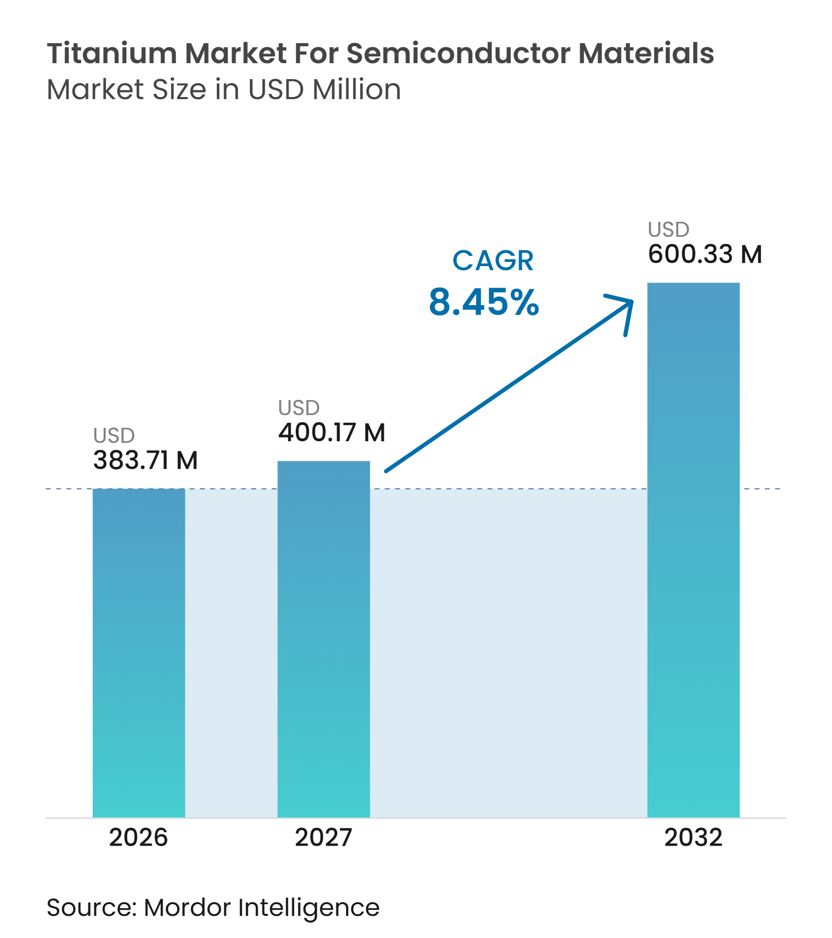
The Titanium Market Size for Semiconductor Materials Industry was valued at USD 383.71 million in 2026 and is estimated to grow from USD 400.17 million in 2027 to reach USD 600.33 million by 2032, at a CAGR of 8.45% during the forecast period (2027-2032). The titanium market for semiconductor materials is supported by the construction of advanced semiconductor fabs, which increases the installed base of physical vapor deposition and chemical vapor deposition equipment. Titanium nitride and titanium dioxide are used as barrier layers, adhesion materials, and work-function metals in wafer processing. Demand is shifting toward higher-value materials because advanced logic and memory devices need more deposition steps and tighter impurity controls. National semiconductor programs in the United States, Europe, Japan, and India are widening the geographic base for qualified materials procurement. The titanium market for semiconductor materials also faces supply risk because high-purity titanium sponge production is concentrated in a limited number of countries, while higher purity grades add material and processing costs.
Key Report Takeaways
- By product type, titanium sputtering targets held 65.13% of the titanium market for semiconductor materials share in 2026, while titanium compounds are forecast to advance at a 9.12% CAGR through 2032.
- By application, wafer fabrication held 71.34% of the titanium market for semiconductor materials share in 2026 and is forecast to advance at a 9.56% CAGR through 2032.
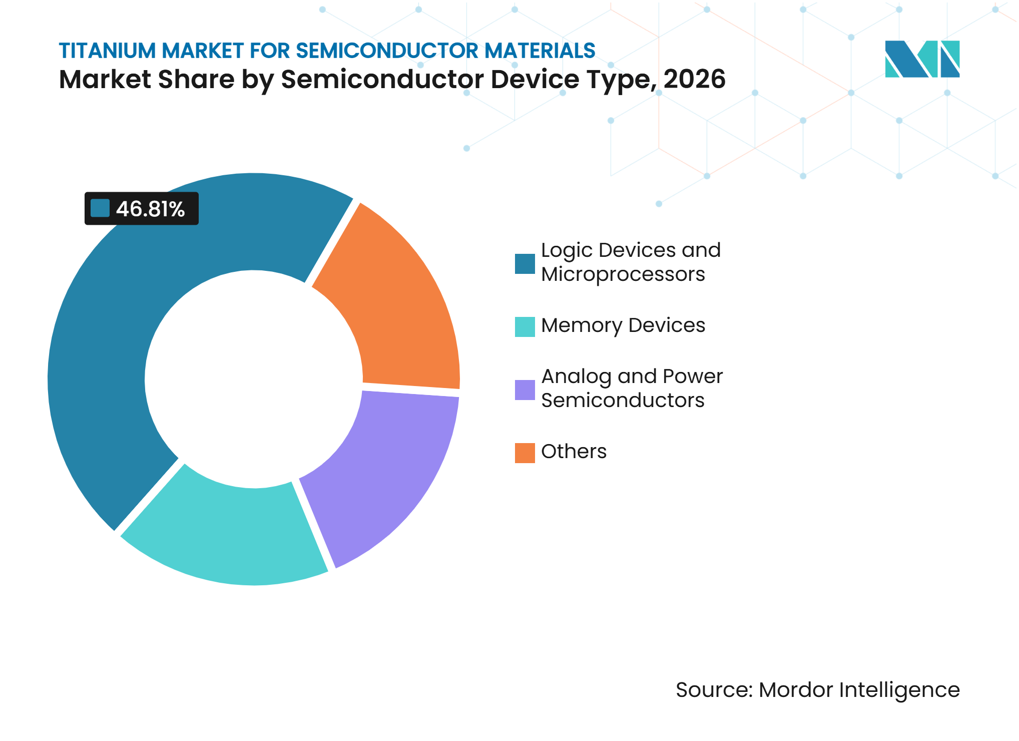
- By semiconductor device type, logic devices and microprocessors held 46.81% of the titanium market for semiconductor materials share in 2026, while memory devices are forecast to advance at a 9.34% CAGR through 2032.
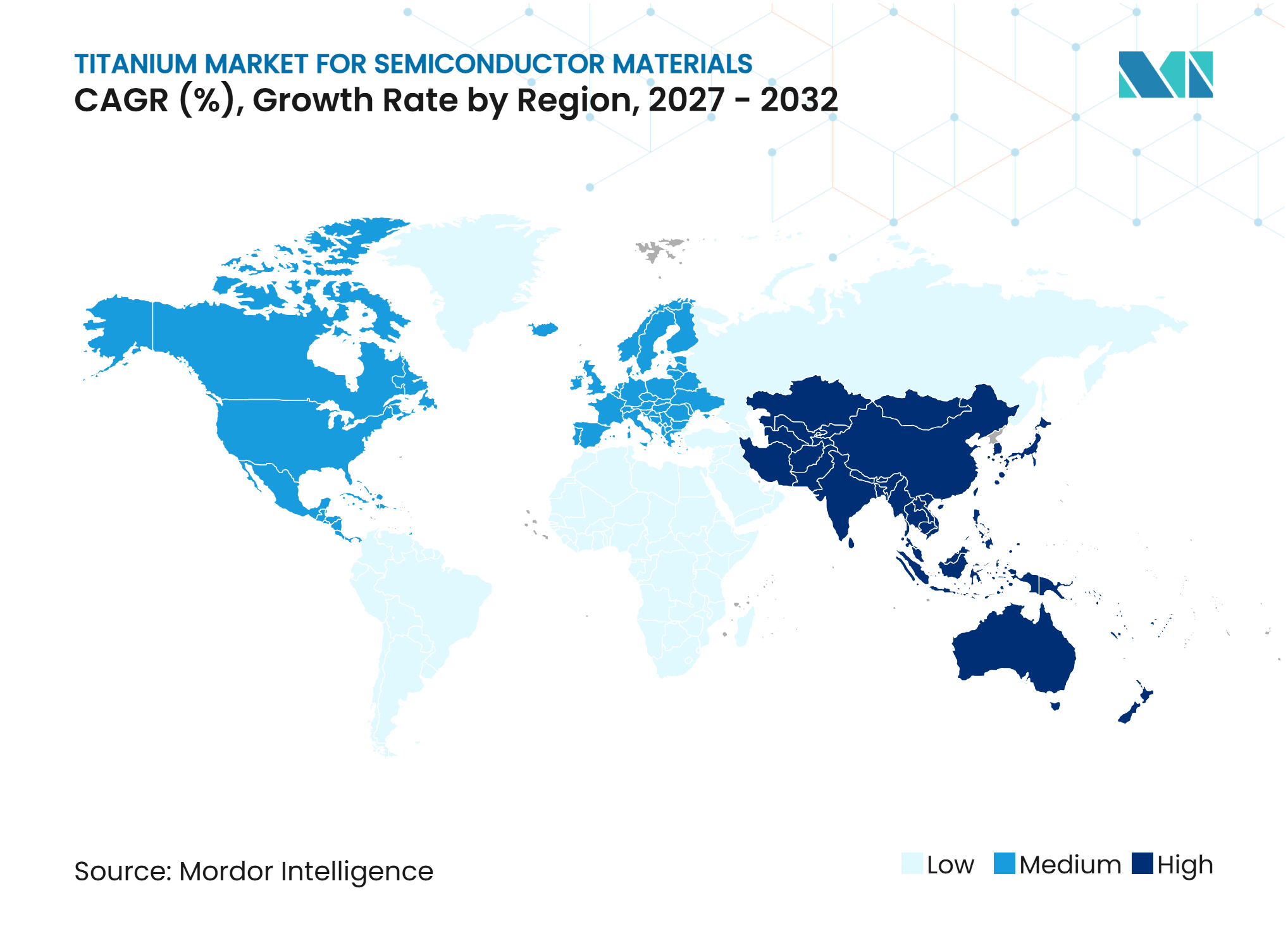
- By geography, Asia-Pacific held 50.28% of the titanium market for semiconductor materials share in 2026 and is forecast to advance at a 9.22% CAGR through 2032.
Note: Market numbers in this report are based on Mordor Intelligence's proprietary estimation framework, which combines nine months of actuals with Q4 projections for base year 2026.
Market Trends and Insights
Drivers Impact Analysis of Titanium Market For Semiconductor Materials*
| Driver | (~) % Impact on CAGR Forecast | Geographic Relevance | Impact Timeline |
|---|---|---|---|
| AI-Driven Advanced Logic and Memory Fab Expansion | +3.5% | Global, led by APAC (Taiwan, South Korea, Japan), North America (USA) | Short term (≤ 2 years) |
| Rising Titanium Content in GAA, 3D NAND, and Advanced Packaging Flows | +2.8% | APAC core, spillover to North America and Europe | Medium term (2-4 years) |
| Semiconductor Supply-Chain Localization | +1.6% | North America, Japan, India, Europe | Medium term (2-4 years) |
| Higher Purity and Lower Particle Requirements at Advanced Nodes | +1.2% | Global, led by APAC leading-edge fabs | Short term (≤ 2 years) |
| Qualification Demand for Local and Dual-Source Suppliers | +0.8% | North America, Europe, Japan | Long term (≥ 4 years) |
| Source: Mordor Intelligence | |||
AI-Driven Advanced Logic and Memory Fab Expansion
Generative artificial intelligence infrastructure is increasing demand for advanced logic and memory capacity, which raises titanium use through greater wafer output and more titanium film steps per wafer. Taiwan Semiconductor Manufacturing Company is ramping its 2-nanometer gate-all-around process, with capacity plans linked to demand from Apple, NVIDIA, Advanced Micro Devices, and Qualcomm. This production shift raises titanium nitride consumption in gate dielectric and barrier-layer stacks. Taiwan Semiconductor Manufacturing Company has also committed USD 165 billion to Arizona facilities that include advanced fabs, packaging capacity, and research and development operations. The titanium market for semiconductor materials can therefore grow faster than total wafer starts when chip value and process complexity rise together. These conditions favor suppliers that can consistently meet advanced-node purity and particle specifications.
Rising Titanium Content in GAA, 3D NAND, and Advanced Packaging Flows
Gate-all-around, three-dimensional NAND, and advanced packaging are increasing titanium material use per processed wafer. Gate-all-around transistor structures use multiple titanium nitride work-function metal layers around nanosheet channels and require conformal deposition. This changes demand toward atomic layer deposition and chemical vapor deposition materials where line-of-sight sputtering is insufficient. Three-dimensional NAND structures with more than 200 layers need titanium-containing barrier films across each tier, which links material use to stack height as well as wafer volume. Through-silicon vias, fan-out wafer-level packaging, and hybrid bonding also add titanium deposition steps in packaging flows. This shift supports the titanium market for semiconductor materials as device complexity rises. JX Advanced Metals Corporation joined the JOINT3 consortium in September 2025 to develop panel-level organic interposer materials and design tools, identifying semiconductor sputtering targets as a growing packaging-related application.
Semiconductor Supply-Chain Localization
Supply-chain localization is changing where titanium materials are qualified, manufactured, and consumed. The United States CHIPS and Science Act provides incentives for domestic semiconductor manufacturing, while the proposed Strengthening Essential Manufacturing and Industrial Investment Act sought to clarify comparable tax-credit treatment for critical-material suppliers. Japan has supported supply assurance for semiconductor sputtering targets through its economic security framework. In July 2025, Japan’s Ministry of Economy, Trade and Industry certified JX Advanced Metals Corporation’s supply assurance plan for its Hitachinaka factory expansion. China’s domestic materials suppliers are also expanding capacity to serve local fabs. The titanium market for semiconductor materials gains new regional demand pools when materials producers establish local qualification and support capability near new fabs.
Qualification Demand for Local and Dual-Source Suppliers
Semiconductor manufacturers are expanding local and dual-source qualification programs to reduce dependence on concentrated materials supply. United States reviews of semiconductor imports and Chinese export-control actions on selected materials increased attention to supply continuity during 2025[1]. Fab operators must still test particle performance, film uniformity, and trace impurity levels before approving an additional titanium source. Qualification creates an opening for regional suppliers, but it does not provide immediate revenue because testing is lengthy. Existing suppliers can gain new business from local clients when they have qualified manufacturing and application support in target geographies. The titanium market for semiconductor materials is therefore becoming more regional in its supply arrangements while remaining technically global.
Restraints Impact Analysis of Titanium Market For Semiconductor Materials*
| Restraint | (~) % Impact on CAGR Forecast | Geographic Relevance | Impact Timeline |
|---|---|---|---|
| High Purification, Melting, and Bonding Costs | -1.0% | Global, most acute in North America and Europe | Short term (≤ 2 years) |
| Long Fab Qualification Cycles and Switching Costs | -0.7% | Global, most acute in leading-edge APAC fabs | Medium term (2-4 years) |
| Ultra-Low Oxygen and Metallic Impurity Control Bottlenecks | -0.4% | Global, most acute in Japan, USA, South Korea | Long term (≥ 4 years) |
| Source: Mordor Intelligence | |||
High Purification, Melting, and Bonding Costs
High-purity titanium sponge must be refined through energy-intensive vacuum arc remelting or electron beam cold hearth remelting before it can be used for advanced target production. Each increase in purity removes a larger share of remaining impurities and raises processing cost. Target bonding also requires close control of temperature and pressure because an imperfect interface can cause target deflection or particle contamination during sputtering. These operating requirements make scale and process know-how important cost advantages. Smaller producers face a more difficult path to competitive manufacturing costs even when local demand is increasing. The titanium market for semiconductor materials therefore remains exposed to high electricity use, specialized equipment needs, and limited ultra-high-purity processing capacity.
Long Fab Qualification Cycles and Switching Costs
Advanced fabs typically require 12 to 24 months of continuous performance testing before accepting a new titanium target supplier. The process evaluates particle performance, film uniformity, and trace impurity profiles under production conditions. A failed test can require the evaluation cycle to restart, creating cost and delay for both the supplier and the fab. This favors established suppliers that already have approved materials for a customer’s process flow. Semiconductor Equipment and Materials International (SEMI) M1 and C3 standards can improve documentation and operational consistency, but they do not remove the need for long materials testing. The titanium market for semiconductor materials consequently has high switching costs even as fabs seek more than one qualified source.
*Our forecasts treat driver/restraint impacts as directional, not additive. The impact forecasts reflect baseline growth, mix effects, and variable interactions.
Titanium Market For Semiconductor Materials Segment Analysis
By Product Type:
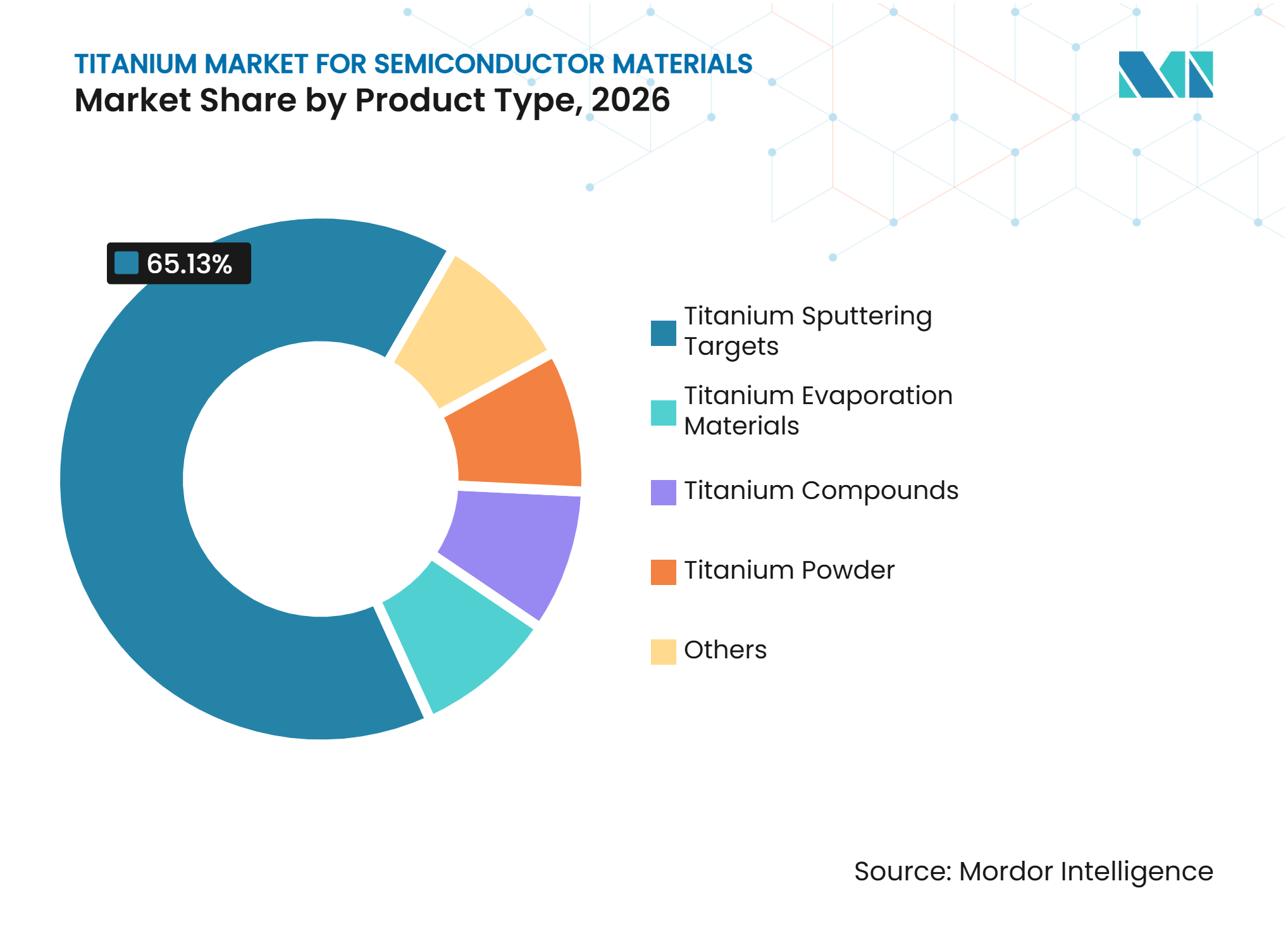
Titanium Sputtering Targets Drive Demand, Titanium Compounds AccelerateTitanium sputtering targets accounted for 65.13% of the market share in 2026. They remain the main deposition material for physical vapor deposition-based barrier and adhesion layers across logic and memory wafer production. At mature process nodes, titanium targets are commonly used for adhesion layers and titanium nitride barrier precursors. At 3 nanometers and below, more deposition steps per wafer increase consumption as device structures become more complex. Titanium evaporation materials and titanium powder serve narrower applications, including gallium nitride device metallization and titanium compound precursor production. These products support specialized demand but have a smaller role than sputtering targets in mainstream wafer fabrication.
Titanium compounds are projected to advance at a 9.12% CAGR through 2032. Demand is linked to the growing use of atomic layer deposition for conformal titanium nitride films at sub-10 nanometer dimensions. Atomic layer deposition provides coverage in high-aspect-ratio structures that conventional sputtering cannot consistently achieve. JX Advanced Metals Corporation completed a mass-production line for high-purity chemical vapor deposition and atomic layer deposition materials at its Ibaraki Office, Hitachi Area, in March 2026 and began shipments to customers. The company stated that the line supports materials used in advanced semiconductor applications and expects higher sales volumes. The titanium market for semiconductor materials industry is therefore moving toward a broader mix of target and compound-form materials.


By Application:
Wafer Fabrication Anchors Both Scale and GrowthWafer fabrication held 71.34% of the market share in 2026. Titanium nitride barrier layers limit copper diffusion into dielectric materials, while titanium adhesion layers support reliable film-to-substrate bonding. Titanium silicide contacts also help reduce source-drain contact resistance in advanced logic devices. Gate-all-around structures increase deposition requirements because individual nanosheet channels need conformal barrier coverage. New fabs create recurring demand for qualified titanium materials once physical vapor deposition systems are installed. Semiconductor Equipment and Materials International reported continued construction activity across global semiconductor manufacturing capacity during 2025.
Wafer fabrication is projected to advance at a 9.56% CAGR through 2032. Its simultaneous leadership in revenue and growth reflects titanium’s central role in front-end process flows rather than a shift toward a newer application. Semiconductor packaging also has a meaningful demand role because through-silicon vias, fan-out wafer-level packaging, and hybrid bonding use titanium films for redistribution-layer metallization and diffusion barriers. The rise of 2.5D and 3D integration in artificial intelligence accelerators increases the number of interfaces that need precise metallization. High-bandwidth memory stacks and chiplet architectures strengthen this requirement in back-end semiconductor processing. This extends the addressable titanium market for semiconductor materials beyond the front-end wafer flow. Compliance with Semiconductor Equipment and Materials International specifications for packaging-grade materials is becoming more important in purchasing decisions.
By Semiconductor Device Type:
Logic Devices and Microprocessors Lead, Memory Devices AccelerateLogic devices and microprocessors held 46.81% of the market share in 2026. Titanium is used in these products as a contact and barrier-layer material at advanced foundries. Custom artificial intelligence application-specific integrated circuits are broadening logic demand beyond central processing units and graphics processing units. This includes chips designed by hyperscale companies for training and inference workloads, as well as edge artificial intelligence processors developed for automotive applications. The ramp of 2-nanometer gate-all-around processes by Taiwan Semiconductor Manufacturing Company and Samsung supports a durable demand base for titanium materials. Capacity investment is increasingly tied to customer commitments, which supports demand visibility for qualified suppliers.
Memory devices are projected to advance at a 9.34% CAGR through 2032. Three-dimensional NAND and high-bandwidth memory increase titanium film requirements because each added layer or die interface needs barrier and contact deposition. Commercial three-dimensional NAND structures now exceed 200 layers, which increases material intensity even when wafer starts do not rise at the same rate. Toho Titanium Co., Ltd. reported strong semiconductor-related demand for high-purity titanium in its fiscal 2025 first-half results. Analog and power semiconductors provide a smaller but stable contribution through gallium nitride and silicon carbide metallization. Other applications include microelectromechanical systems and photonics, while ISO 14001 requirements are increasingly relevant to supplier environmental management practices.
Geography Analysis
Asia-Pacific
Asia-Pacific held a 50.28% share in 2026 and is projected to advance at a 9.22% CAGR through 2032. Taiwan remains central to leading-edge logic production as Taiwan Semiconductor Manufacturing Company expands gate-all-around capacity. South Korea supports memory-related demand through Samsung and SK Hynix, where high-bandwidth memory and three-dimensional NAND require repeated barrier-layer deposition. Japan remains a key materials manufacturing base, and JX Advanced Metals Corporation has expanded high-purity chemical vapor deposition and atomic layer deposition material capacity at its Ibaraki site. Japan’s Ministry of Economy, Trade and Industry certification of the company’s supply assurance plan shows the regulatory influence of the Economic Security Promotion Act on semiconductor materials capacity. China is expanding domestic material supply to serve its semiconductor base, increasing the importance of local qualification and capacity utilization. These conditions keep the region important for both titanium production and consumption.
North America
North America is developing additional titanium materials demand as new semiconductor plants enter production and others progress toward operation. Taiwan Semiconductor Manufacturing Company began high-volume manufacturing at its Arizona Fab 1 during 2025, and the company is developing further United States capacity for advanced processes. Intel is also advancing Arizona production capacity for its 18A process generation. Every new physical vapor deposition tool requires qualified target materials, which creates a local procurement opportunity after commissioning. Solstice Advanced Materials broke ground on a USD 200 million Spokane Valley expansion in December 2025 and expects to double sputtering-target production capacity by 2029. The proposed tax-credit clarification for critical-material suppliers supports the case for investment near United States fabs. Supply assurance and domestic manufacturing are becoming important factors alongside product purity and performance.
Europe, South America, and Middle East and Africa
Europe has semiconductor materials demand from planned manufacturing investments, including facilities associated with Intel in Germany and Taiwan Semiconductor Manufacturing Company in Dresden. The region remains dependent on imports for some high-purity titanium materials because local production capacity is limited. The European Commission’s Joint Research Centre called for greater supply diversification and titanium recycling partnerships, pointing to resource security as an emerging policy concern[2]. Plansee SE provides European technical capability in powder-metallurgy-based titanium target production for semiconductor applications. South America has smaller demand that is primarily related to semiconductor assembly activities in Mexico and Brazil. Middle East and Africa demand is at an earlier stage, with Saudi Arabia’s diversification programs and Israel’s specialty chip ecosystem providing a foundation for future activity. These geographies form a longer-term demand pipeline as semiconductor investment becomes less concentrated in Asia-Pacific.
Competitive Landscape
Market Concentration
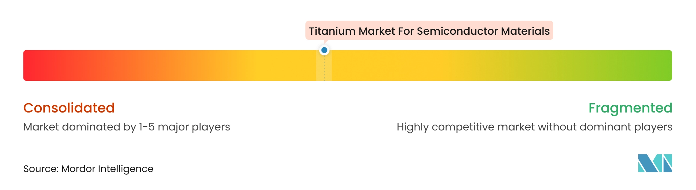
The titanium market for semiconductor materials is moderately concentrated, with the top five players including JX Advanced Metals Corporation, Materion Corporation, Tosoh Corporation, Plansee SE, and ULVAC, Inc. In February 2026, JX Advanced Metals Corporation and Toho Titanium Co., Ltd. announced a share exchange agreement that would make Toho Titanium Co., Ltd. a wholly owned subsidiary of JX Advanced Metals Corporation, effective June 1, 2026. The transaction supports tighter control of high-purity titanium sponge and precursor materials. Konfoong Materials International Co., Ltd. is strengthening its position through high-purity target capacity and development work for advanced-node applications. The leading companies are competing through metallurgical control, customer qualification, and the ability to serve regional supply-chain needs.
Regional policy is adding another dimension to supplier competition in the titanium market for semiconductor materials. Solstice Advanced Materials is expanding its Spokane Valley facility to serve semiconductor demand with more domestic production capacity. JX Advanced Metals Corporation is using its Ministry of Economy, Trade and Industry-certified supply assurance plan to expand the Hitachinaka factory. Materion Corporation completed an acquisition to expand its semiconductor footprint and capabilities in Asia during 2025. Plansee SE has continued work on target design and process innovation. Semiconductor Equipment and Materials International C3 and M1 standards, together with ISO 9001 quality management certification, remain important compliance factors for serious participants.
The companies address a mix of semiconductor targets, specialized alloy products, process materials, equipment-linked supply, research-grade demand, and regional customer requirements. Sumitomo Chemical Co., Ltd. agreed to acquire Asia Union Electronic Chemical Corporation in November 2025 to expand its semiconductor process chemicals manufacturing presence in Taiwan. Niterra Materials Co., Ltd. was integrated into the Niterra Group during 2025, expanding the group’s advanced materials activities in power semiconductor packaging. Competitive outcomes will depend on product quality, reliability, local support, and success in qualifying materials for advanced device generations.
Leaders of Titanium Market For Semiconductor Materials
-
JX Advanced Metals Corporation
-
Materion Corporation
-
Tosoh Corporation
-
Plansee SE
-
ULVAC, Inc.
- *Disclaimer: Major Players sorted in no particular order
Titanium Market For Semiconductor Materials Companies Covered in this Report
- ALB Materials Inc.
- Hitachi Metals, Ltd.
- Jiangxi Ketai Advanced Materials Co., Ltd.
- JX Advanced Metals Corporation
- Konfoong Materials International Co., Ltd.
- Kurt J. Lesker Company
- Materion Corporation
- Mitsui Kinzoku Co., Ltd.
- Niterra Materials Co., Ltd.
- Plansee SE
- Solstice Advanced Materials
- Sumitomo Chemical Co., Ltd.
- Toho Titanium Co., Ltd.
- Tosoh Corporation
- ULVAC, Inc.
Recent Industry Developments in Titanium Market For Semiconductor Materials
- July 2026: JX Advanced Metals Corporation announced an investment of approximately JPY 4 billion (USD 24.6 million) to expand semiconductor sputtering target processing capacity at its South Korean subsidiary, JX Advanced Metals Korea Co., Ltd. The expansion is expected to double processing capacity compared with fiscal 2025 levels, with operations scheduled to begin in phases from the second half of fiscal 2027, supporting the titanium market for semiconductor materials through improved processing capacity and supply availability for advanced semiconductor targets.
- December 2025: Solstice Advanced Materials broke ground on a USD 200 million expansion and modernization project at its electronic materials facility in Spokane Valley, Washington. The investment is expected to double the facility's sputtering target production capacity by the end of 2029 and reduce lead times by 25%, supporting the titanium market for semiconductor materials through expanded domestic manufacturing of specialized sputtering targets and semiconductor materials.
Scope of Report on Titanium Market For Semiconductor Materials
Titanium is a refractory metal valued for its high melting point, corrosion resistance, and ability to form stable compounds and thin films. These properties make it useful in semiconductor manufacturing, where high-purity titanium materials support specialized deposition and fabrication processes.
The Titanium Market for Semiconductor Materials is segmented by product type, application, semiconductor device type, and geography. By product type, the market is segmented into titanium sputtering targets, titanium evaporation materials, titanium powder, titanium compounds, and others. By application, the market is segmented into wafer fabrication and semiconductor packaging. By semiconductor device type, the market is segmented into logic devices and microprocessors, memory devices, analog and power semiconductors, and others. The report also covers the market size and forecasts for titanium for semiconductor materials across 16 countries. For each segment, the market sizing and forecasts have been done on the basis of value (USD).
Segmentation Overview
| Titanium Sputtering Targets |
| Titanium Evaporation Materials |
| Titanium Powder |
| Titanium Compounds |
| Others |
| Wafer Fabrication |
| Semiconductor Packaging |
| Logic Devices and Microprocessors |
| Memory Devices |
| Analog and Power Semiconductors |
| Others |
| Asia-Pacific | China |
| India | |
| Japan | |
| South Korea | |
| ASEAN Countries | |
| Rest of Asia-Pacific | |
| North America | United States |
| Canada | |
| Mexico | |
| Europe | Germany |
| United Kingdom | |
| France | |
| Italy | |
| NORDIC Countries | |
| Russia | |
| Rest of Europe | |
| South America | Brazil |
| Argentina | |
| Rest of South America | |
| Middle East and Africa | Saudi Arabia |
| South Africa | |
| Rest of Middle East and Africa |
| By Product Type | Titanium Sputtering Targets | |
| Titanium Evaporation Materials | ||
| Titanium Powder | ||
| Titanium Compounds | ||
| Others | ||
| By Application | Wafer Fabrication | |
| Semiconductor Packaging | ||
| By Semiconductor Device Type | Logic Devices and Microprocessors | |
| Memory Devices | ||
| Analog and Power Semiconductors | ||
| Others | ||
| By Geography | Asia-Pacific | China |
| India | ||
| Japan | ||
| South Korea | ||
| ASEAN Countries | ||
| Rest of Asia-Pacific | ||
| North America | United States | |
| Canada | ||
| Mexico | ||
| Europe | Germany | |
| United Kingdom | ||
| France | ||
| Italy | ||
| NORDIC Countries | ||
| Russia | ||
| Rest of Europe | ||
| South America | Brazil | |
| Argentina | ||
| Rest of South America | ||
| Middle East and Africa | Saudi Arabia | |
| South Africa | ||
| Rest of Middle East and Africa | ||
Key Questions Answered in the Report
What is the size of the titanium market for semiconductor materials?
The titanium market for semiconductor materials industry size was valued at USD 383.71 million in 2026 and is estimated to grow from USD 400.17 million in 2027 to reach USD 600.33 million by 2032, at a CAGR of 8.45% during the forecast period (2027-2032).
What is driving demand for titanium semiconductor materials?
New advanced fabs, artificial intelligence-related logic and memory demand, and higher titanium use in gate-all-around and three-dimensional NAND processes are supporting growth.
Which product type held the largest share in 2026?
Titanium sputtering targets led with a 65.13% share in 2026 because they are widely used in physical vapor deposition for barrier and adhesion layers.
Which application is expected to grow fastest through 2032?
Wafer fabrication is projected to advance at a 9.56% CAGR through 2032, supported by new fab construction and more complex front-end process flows.