
Thin-Film Electrode Market Size and Share
Market Overview
| Study Period | 2022 - 2032 |
|---|---|
| Market Size (2027) | USD 0.72 Billion |
| Market Size (2032) | USD 1.22 Billion |
| Growth Rate (2027 - 2032) | 11.13 % |
| Fastest Growing Market | Asia-Pacific |
| Largest Market | Asia-Pacific |
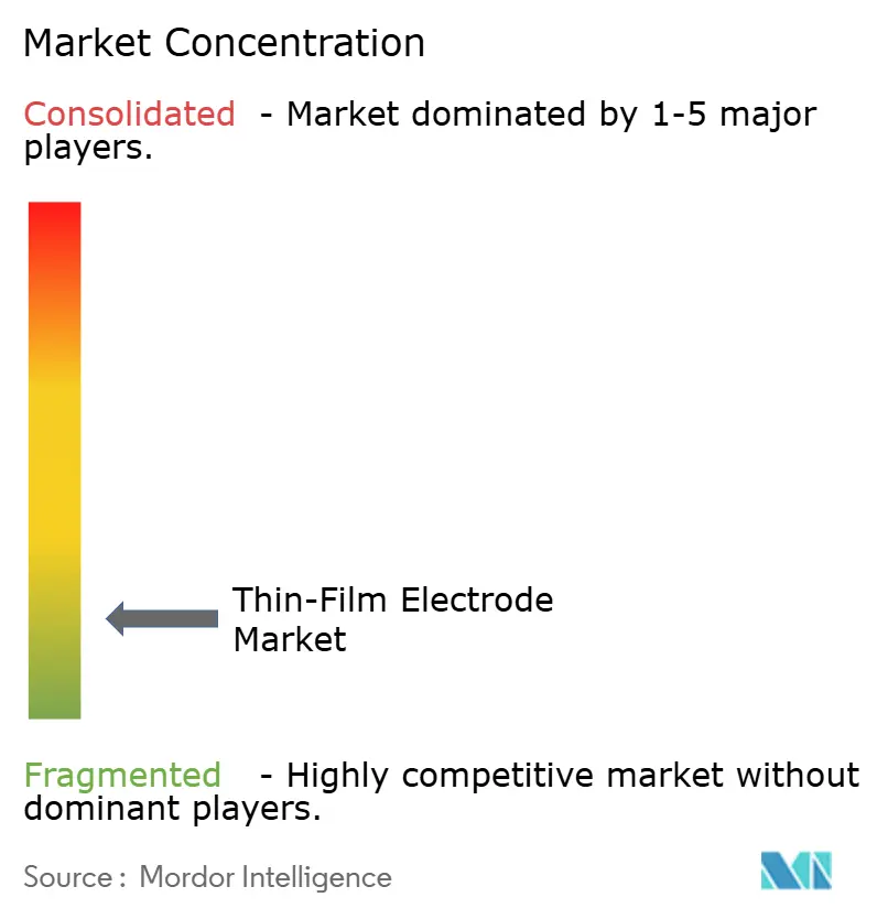
| Market Concentration | Low |
Major Players *Disclaimer: Major Players sorted in no particular order Image © Mordor Intelligence. Reuse requires attribution under CC BY 4.0. | |
Thin-Film Electrode Market Analysis by Mordor Intelligence
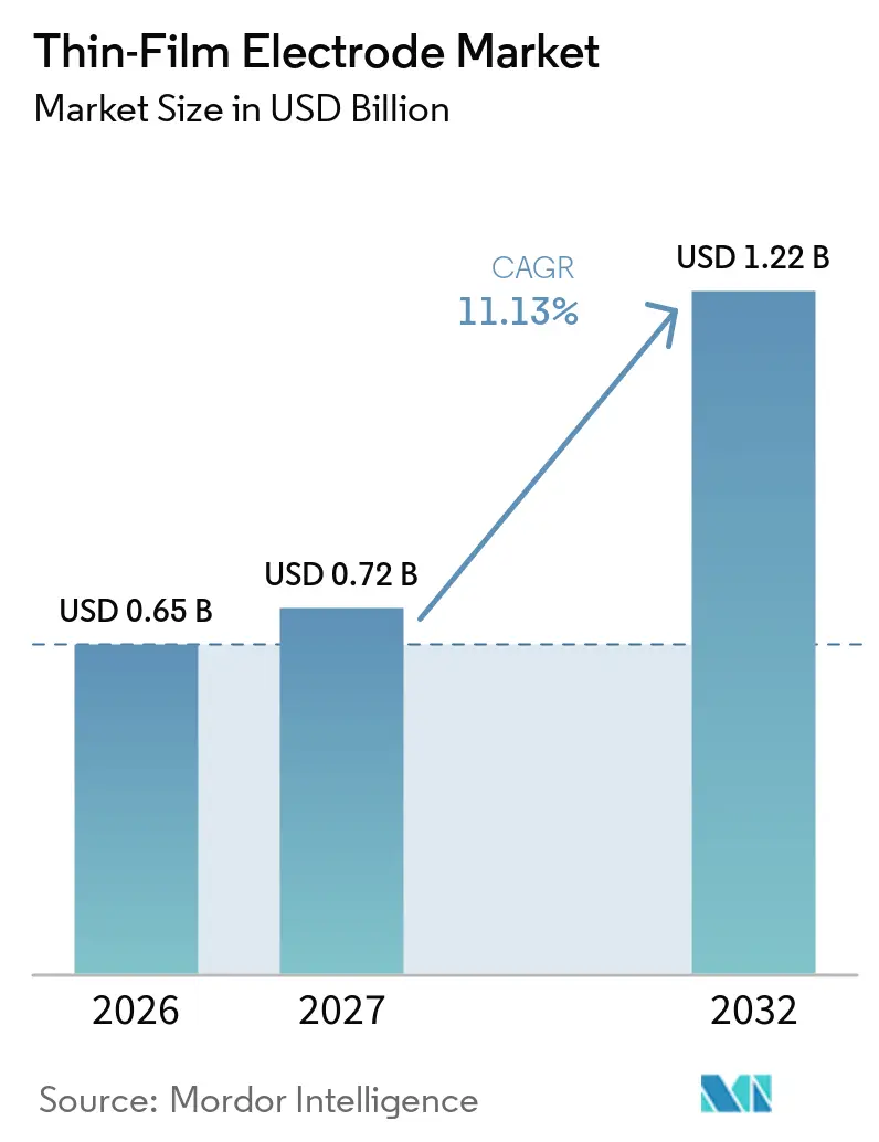
The thin-film electrode market size was valued at USD 0.65 billion in 2026 and is estimated to grow from USD 0.72 billion in 2027 to reach USD 1.22 billion by 2032, at a CAGR of 11.13% during the forecast period (2027-2032). The thin-film electrode market is driven by demand from semiconductor manufacturing, wearable health devices, microsensors, solid-state batteries, and electrochemical equipment. Device producers increasingly require conductive layers that can be deposited with precise thickness control on compact substrates. This requirement supports adoption in advanced logic, memory, and sensing devices, where electrode design affects yield and device performance. Suppliers are responding with greater process integration, material qualification, and expanded manufacturing capacity. The market also benefits from customer demand for smaller devices that maintain electrical performance and reliability.
Key Report Takeaways
- By material, metal-based electrodes held 52.16% of the thin-film electrode market share in 2026, while carbon-based electrodes are forecast to expand at a 12.45% CAGR through 2032.
- By manufacturing technology, physical vapor deposition held 58.45% share in 2026, while electrochemical deposition and electroplating are forecast to expand at a CAGR of 12.78% through 2032.
- By end-user industry, electronics and semiconductor held 46.38% share in 2026 and are forecast to expand at a CAGR of 13.14% through 2032.
- By geography, Asia-Pacific held 45.92% share in 2026 and is forecast to expand at a CAGR of 12.82% through 2032.
Note: Market numbers in this report are based on Mordor Intelligence's proprietary estimation framework, which combines nine months of actuals with Q4 projections for base year 2026.
Global Thin-Film Electrode Market Trends and Insights
Drivers Impact Analysis*
| Drivers | (~) % Impact on CAGR Forecast | Geographic Relevance | Impact Timeline |
|---|---|---|---|
| Rising Demand for Miniaturized and Flexible Electronics | +2.8% | Global, concentrated in Asia-Pacific, Taiwan, South Korea, China, and North America | Medium term (2-4 years) |
| Expansion of Biosensors, Wearable Diagnostics, and Point-of-Care Testing | +1.9% | Global, with early gains in North America, Europe, and East Asia | Medium term (2-4 years) |
| Semiconductor, Display, and Advanced Packaging Investments | +2.5% | Asia-Pacific core, with spillover to North America and Europe | Short term (≤ 2 years) |
| Solid-State Battery and Distributed Energy Storage Commercialization | +1.6% | Global, led by Japan, South Korea, France, and North America | Long term (≥ 4 years) |
| High-Throughput Roll-to-Roll and Wafer-Level Electrode Manufacturing | +1.3% | Asia-Pacific and North America | Medium term (2-4 years) |
| Source: Mordor Intelligence | |||
Rising Demand for Miniaturized and Flexible Electronics
The thin-film electrode market benefits from electronic designs operating below 1 μm without sacrificing signal quality. Flexible substrates can accommodate dimensions consistent with established semiconductor design requirements. Thin-film electrode suppliers can therefore address wearables, flexible displays, and compact sensor assemblies with related deposition capabilities. MXene composite electrodes made by dispensing printing have also demonstrated width control between 150 μm and 500 μm for wearable glucose and biomarker sensing patches. This combination of dimensional control and flexible form factors broadens the addressable applications for thin-film electrode designs.
The thin-film electrode market is also affected by the need to place sensing functions closer to the user or device surface. Flexible layers can conform to curved surfaces that would be difficult for rigid components to serve. This supports the use of electrodes in skin patches, compact diagnostic devices, and connected sensor systems. The same manufacturing methods can be used across different product formats when the substrate and interface requirements are compatible. Producers that maintain repeatable film thickness and adhesion can reduce the development burden for customers moving across these applications. As flexible electronics approach conventional semiconductor performance expectations, the distinction between the two application groups becomes less clear.
Expansion of Biosensors, Wearable Diagnostics, and Point-of-Care Testing
The thin-film electrode market benefits from point-of-care systems that need sensitive measurements from small sample volumes. A 2025 study reported that disposable thin-film electrodes made by shadow-mask physical vapor deposition detected C-reactive protein in human serum with a 6.5 pg/mL limit of detection. Such designs can work with sample drops of 1 μL to 10 μL while preserving electrochemical measurement capability. This is useful for portable diagnostic systems that cannot rely on large sample preparation steps. Thin films also enable the incorporation of signal-processing functions into flexible polymer structures. These attributes support long-duration health monitoring where device comfort and low-profile construction matter.
The thin-film electrode market is supported by wearable platforms that measure cortisol, sodium, and glucose levels, as well as ECG, EMG, and EEG signals. Skin-interfacing electrodes reported in 2025 achieved signal-to-noise ratios up to 38 dB and interface impedances an order of magnitude below clinical gel standards[1]. Better signal quality during movement can improve the practical use of wearable devices beyond controlled clinical settings. Suppliers must still demonstrate biocompatibility, stability, and repeatable electrical behavior across the use period. These requirements favor electrode materials with established performance histories, including gold and platinum-based formulations. The resulting qualification work can make the biosensor segment demanding, but it can also support recurring demand from approved platforms.
Semiconductor, Display, and Advanced Packaging Investments
The thin-film electrode market is closely tied to investments in wafer fabrication, display production, and advanced packaging. Tokyo Electron reported an all-time high fiscal year 2025 net sales of JPY 2,431.5 billion (~USD 15.34 billion), supported by AI server logic and high-bandwidth memory customers. These programs require deposition processes capable of forming uniform conductive layers at increasingly small dimensions. Gate-all-around designs and high-layer-count 3D NAND add deposition steps that bulk electrode methods cannot perform. Each added step increases the importance of process control, film adhesion, and contamination management. The thin-film electrode market, therefore, follows the technology intensity of new chip architectures, not only the number of wafers produced.
Applied Materials invested USD 2.26 billion in capital expenditure and USD 3.57 billion in research and development during fiscal year 2025. Merck KGaA also invested EUR 500 million (~USD 558.66 million) in its Kaohsiung semiconductor materials site, with production planned for 2026. These commitments indicate that material and equipment suppliers are preparing capacity before customer demand is fully realized. They also increase the importance of reliable access to high-purity precursors and sputtering targets. For the thin-film electrode market, this environment rewards suppliers that can qualify materials and processes early in customer development cycles. It also raises the cost of competing where customers require proven performance across multiple process steps.
Solid-State Battery and Distributed Energy Storage Commercialization
The thin-film electrode market is gaining further demand from solid-state batteries and distributed energy storage systems. In these applications, electrode architecture influences ionic transport, interfacial resistance, power delivery, and cycle life. ITEN reported in April 2025 that its full-ceramic thin-film electrodes achieved a 200C discharge rate, delivering 30 mA pulses over 50 milliseconds on an 18 mm² footprint. This result illustrates how thin-film structures can provide high power within a very small area. Such capabilities can support compact electronics that require brief but intense power delivery. Energy applications can therefore reduce dependence on any single end-user category.
Atomic layer deposition is also relevant because surface coatings can improve the performance of cathode and anode materials. Forge Nano raised USD 40 million in May 2025 for its atomic layer deposition coating technology, which has applications in battery materials and semiconductor wafer processing. The crossover between energy storage and semiconductor processing gives equipment and material suppliers several potential routes to commercialization. Battery applications require consistent coverage across complex surfaces and stable interfaces under repeated cycling. Thin-film electrode producers that meet these requirements can participate in battery pilot lines as they move toward larger-scale production. The thin-film electrode market thus gains demand from systems that need both miniaturization and energy storage performance.
Restraints Impact Analysis*
| Restraints | (~) % Impact on CAGR Forecast | Geographic Relevance | Impact Timeline |
|---|---|---|---|
| High Capital Intensity of Deposition and Cleanroom Manufacturing | -0.8% | Global, most acute for emerging-market entrants in South and Southeast Asia | Long term (≥ 4 years) |
| Precious Metal, High-Purity Target, and Critical-Mineral Price Volatility | -0.6% | Global, with heightened exposure in Asia-Pacific production hubs | Medium term (2-4 years) |
| Qualification Bottlenecks for Medical and Semiconductor Applications | -0.4% | North America, Europe, and the Asia-Pacific advanced fabs | Medium term (2-4 years) |
| Substrate Reliability and Thermal-Stress Failure in Large-Area and Harsh-Environment Systems | -0.3% | Asia-Pacific, the Middle East, and Africa for high-temperature industrial deployments | Long term (≥ 4 years) |
| Source: Mordor Intelligence | |||
High Capital Intensity of Deposition and Cleanroom Manufacturing
The thin-film electrode market has high entry requirements because competitive production combines deposition tools, lithography, inspection systems, and controlled cleanroom operations. A full production line may require physical or chemical vapor deposition and related patterning equipment before the first qualified batch can ship. Applied Materials reported USD 2.26 billion in capital expenditure for fiscal year 2025, illustrating the scale of investment associated with equipment operations[2]. Smaller suppliers focused on biosensors or analytical systems face a significant gap between pilot equipment and certified production capacity. This gap persists even when customer demand is strong and can limit the number of new suppliers that reach commercial scale.
Roll-to-roll methods may reduce some cost burdens for flexible-substrate products, but they do not eliminate the expense of precise deposition and controlled production conditions. Systems designed to maintain sub-micron film uniformity require specialized equipment and process expertise. Suppliers in the thin-film electrode market must also validate electrical performance, adhesion, surface chemistry, and durability for each target application. Capital recovery can take longer when customer qualification cycles delay orders. This favors firms with established facilities and broad product portfolios and makes partnerships with equipment, materials, and application specialists more important for new entrants.
Precious Metal, High-Purity Target, and Critical-Mineral Price Volatility
The thin-film electrode market is exposed to input costs for gold, platinum, titanium, ruthenium, tungsten, and other high-purity materials. These inputs can be affected by supply disruptions, geopolitical trade flows, and demand from adjacent industries. In September 2025, JX Metals projected that its sales of semiconductor thin-film materials for 3D NAND applications would triple. Higher demand for high-purity materials can tighten target supply if refining capacity does not increase at the same pace. This exposure is particularly relevant for electrodes that require precious metals or tightly controlled material purity. Contract terms may prevent suppliers from immediately passing higher material costs to customers.
Ruthenium and molybdenum are becoming more relevant in advanced electrode applications where faster electron movement is required. Their processing chains can be geographically concentrated, which increases supply risk for manufacturers. The thin-film electrode market must also manage compliance requirements that increase costs for material sourcing and processing. Suppliers may respond by entering into longer procurement agreements and pursuing recycling, material substitution, and closer coordination with customers. These measures can reduce exposure but may not fully eliminate it. Cost volatility, therefore, remains a constraint on margins and investment decisions across the value chain.
*Our forecasts treat driver/restraint impacts as directional, not additive. The impact forecasts reflect baseline growth, mix effects, and variable interactions.
Segment Analysis
By Material: Metal-Based Electrodes Lead Revenue While Carbon-Based Electrodes Accelerate
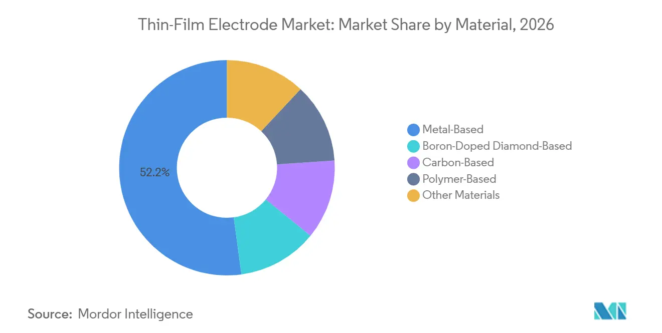
Metal-based electrodes held 52.16% of the thin-film electrode market share in 2026. Gold, platinum, titanium nitride, and tungsten are widely used due to their conductivity, corrosion resistance, and biocompatibility. These properties make them suitable for semiconductor gate contacts, medical implant surfaces, and biosensor working electrodes. Platinum-group targets are commonly used for reference electrodes in thin-film biosensor designs, while gold is used in self-assembled monolayers and aptamer-based diagnostic platforms. The market size for metal-based electrodes reflects their use across multiple demanding applications rather than dependence on a single end use.
Other material classes address specific performance requirements. Boron-doped diamond electrodes are used in high-potential electrochemistry, per- and polyfluoroalkyl substances (PFAS) treatment, and industrial wastewater systems. Polymer electrodes, such as PEDOT:PSS, enable soft bioelectronic interfaces in which mechanical compatibility with tissue is important. Carbon-based materials include graphene, reduced graphene oxide, carbon nanotubes, laser-induced graphene, and MXene composites. A 2025 study reported graphene thin-film networks with conductivity above 1.2 × 10⁵ S/m at a thickness of 11 nm. Carbon-based electrodes are forecast to grow at a CAGR of 12.45% from 2027 to 2032 as these materials expand into a broader range of sensing and electronic applications.

By Manufacturing Technology: Physical Vapor Deposition Leads While Electrochemical Deposition Accelerates
Physical vapor deposition held 58.45% of the market share in 2026. It is used for complex multilayer stacks due to its high deposition rates, adhesion, and multi-target capability. Semiconductor fabs use sputtered titanium nitride, aluminum, and platinum across transistor and interconnect processes. Physical vapor deposition is embedded in established process recipes for logic and memory production. This installed base supports its position in the thin-film electrode market and creates high switching costs for customers considering alternative electrode formation methods.
Electrochemical deposition and electroplating are forecast to grow at a CAGR of 12.78% from 2027 to 2032. These methods support copper damascene interconnects, through-silicon-via filling, and certain battery electrode applications without requiring vacuum infrastructure. Umicore supplies sputtering targets and electroplating chemistries for advanced packaging, compound semiconductors, and silicon front-end processes. Chemical vapor deposition remains relevant for boron-doped diamond synthesis and organometallic precursor applications. Atomic layer deposition is used near gate oxide layers and for battery coatings where conformal coverage is required. The thin-film electrode market relies on multiple deposition technologies, selected based on the material, substrate, and required device performance.
By End-User Industry: Electronics and Semiconductors Drive Demand and Technology Requirements
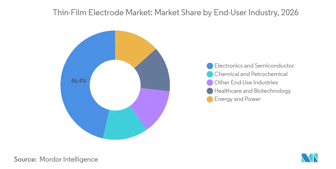
Electronics and semiconductors held 46.38% of the market share in 2026 and are forecast to grow at a CAGR of 13.14% through 2032. Each transition in transistor architecture adds electrode deposition requirements. Gate-all-around structures require sidewall contacts, while 3D NAND involves repeated word-line deposition cycles. These designs require consistent film properties across increasingly complex structures. Applied Materials reported USD 20.8 billion in fiscal year 2025 revenue for its Semiconductor Systems division. The thin-film electrode market reflects the growing complexity of these device processes.
Healthcare and biotechnology represent the second-largest end-user group, supported by demand for biosensors and wearable diagnostics. Energy and power applications include solid-state batteries, fuel cells, and electrochemical reactors. Chemical and petrochemical users employ boron-doped diamond electrodes for industrial wastewater treatment and the destruction of per- and polyfluoroalkyl substances (PFAS). Element Six reported a 99.996% total PFAS reduction in 2025 using its Diamox technology in Lummus Technology Zimpro electro-oxidation systems. These applications broaden the thin-film electrode market beyond semiconductor capital spending and reward suppliers that can tailor surface chemistry, substrate design, and electrical performance to specific operating conditions.
Geography Analysis
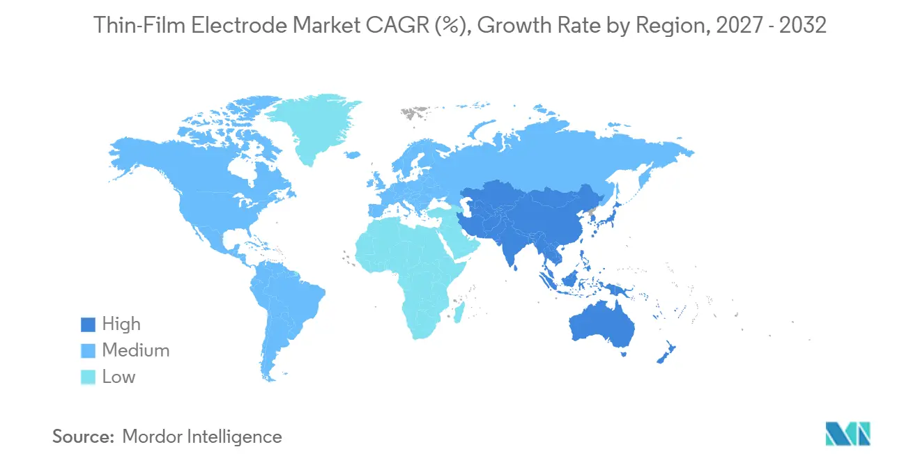
Asia-Pacific held a 45.92% share in 2026 and is forecast to expand at a 12.82% CAGR through 2032. The region benefits from its concentration of wafer fabs, display plants, and advanced packaging sites. This proximity reduces logistics complexity and shortens supplier qualification cycles. Taiwan and South Korea together accounted for 44% of Applied Materials' fiscal year 2025 revenue, or USD 12.5 billion. China accounted for 30% of the company's fiscal year 2025 revenue, underscoring the continued scale of regional semiconductor demand.
Japan, South Korea, Taiwan, and China remain important sources of demand for materials, equipment, and devices in the thin-film electrode market. JX Metals Corporation expects a significant increase in thin-film material sales for 3D NAND applications. India is attracting initial fab commitments under the National Semiconductor Mission. Malaysia and Singapore are developing medical device manufacturing clusters that can increase demand for healthcare-grade electrodes. Export-oriented manufacturers also need to meet materials rules that affect product selection for European customers. These conditions support regional demand for qualified thin-film materials and deposition processes.
North America holds the second-largest regional position, supported by semiconductor fabs, biomedical device original equipment manufacturers, and energy storage research. Applied Materials spent USD 3.57 billion on research and development in fiscal year 2025, much of it associated with North American process innovation. The Texas Semiconductor Innovation Fund granted USD 3.08 million to Tokyo Electron US Holdings for an Austin research and development center in 2025. Europe contributes through clean-energy applications, advanced chemical manufacturing, and research. Merck KGaA is expanding semiconductor material capacity in Asia while retaining European research capabilities. France also has a specialized position through ITEN's thin-film ceramic battery production. South America, the Middle East, and Africa remain smaller opportunities, with Brazil and Saudi Arabia supported by demand for healthcare diagnostics and industrial water treatment.
Competitive Landscape
The thin-film electrode market is moderately fragmented, with suppliers operating across different stages of the value chain. Large equipment and materials companies serve semiconductor customers that require deposition accuracy, scale, and integrated process support. Specialist manufacturers focus on biosensors, analytical chemistry, and energy applications that require tailored electrode functionalization and substrate options. Applied Materials and Tokyo Electron are equipment suppliers in semiconductor deposition. Their installed base and continued research investment make it difficult for new competitors to displace established process recipes. The thin-film electrode market, therefore, combines large-scale equipment leadership with specialized electrode competition.
Applied Materials introduced the Centura Xtera Epi system in October 2025 with integrated pre-clean and etch chambers for void-free gate-all-around source-drain deposition. Merck KGaA inaugurated its Semiconductor Solutions megasite in Kaohsiung in December 2025 following a EUR 500 million (~USD 558.66 million) investment. Umicore supports customers through a combined offering of sputtering targets and electroplating chemistries. These developments indicate that suppliers are pursuing process integration, capacity expansion, and broader materials offerings. In the thin-film electrode market, customer preference for fewer qualified suppliers increases the value of such integrated offerings.
MicruX Technologies, Metrohm DropSens, and PalmSens compete in biosensor electrode niches through functionalization capabilities, catalog range, and distribution access. PalmSens has worked with Linxens Healthcare on roll-to-roll printed-circuit-board electrodes for wearable sensing applications. Ateios Systems and Eastman Kodak announced a solvent-free electrode manufacturing approach operating at 80 meters per minute, with reported energy use reductions of 30% to 40% and a factory footprint reduction of up to 15% compared with wet-process alternatives. These developments highlight the importance of production efficiency and repeatability alongside deposition precision. Qualification requirements in medical devices and semiconductor fabs remain a barrier for suppliers without established operating histories.
Thin-Film Electrode Industry Leaders
-
BASi Research Products, Inc.
-
MicruX Technologies
-
Metrohm DropSens
-
Merck KGaA
-
Applied Materials, Inc.
- *Disclaimer: Major Players sorted in no particular order
Recent Industry Developments
- December 2025: Merck KGaA inaugurated its Semiconductor Solutions megasite in Kaohsiung, Taiwan, with a total investment of EUR 500 million (~USD 558.66 million). The 150,000 m² campus focused on thin-film materials, specialty gases, and formulation materials for advanced logic and memory chip production, supporting thin-film electrode manufacturing, with production beginning in 2026.
- October 2025: Applied Materials unveiled next-generation chipmaking products, including the Centura Xtera Epi system with integrated pre-clean and etch chambers for void-free gate-all-around source-drain deposition. The system recorded 50% lower gas usage and greater than 40% improvement in cell-to-cell uniformity compared to conventional epi systems, enhancing thin-film electrode deposition precision.
Global Thin-Film Electrode Market Report Scope
A thin-film electrode (TFE) is an electrical conductor or sensor manufactured by depositing a thin layer of active material, ranging from a few nanometers to hundreds of micrometers thick, onto a rigid or flexible substrate such as glass, silicon, plastic, or ceramic.
The thin-film electrode market is segmented by material, manufacturing technology, end-user industry, and geography. By material, the market is segmented into metal-based, boron-doped diamond-based, carbon-based, polymer-based, and other materials. By manufacturing technology, the market is segmented into physical vapor deposition, chemical vapor deposition, atomic layer deposition, electrochemical deposition and electroplating, and other manufacturing technologies. By end-user industry, the market is segmented into electronics and semiconductor, healthcare and biotechnology, energy and power, chemical and petrochemical, and other end-use industries. The report also covers market sizes and forecasts for the thin-film electrode across 15 countries in major regions. The market sizes and forecasts are provided in terms of value (USD).
| Metal-Based |
| Boron-Doped Diamond-Based |
| Carbon-Based |
| Polymer-Based |
| Other Materials |
| Physical Vapor Deposition |
| Chemical Vapor Deposition |
| Atomic Layer Deposition |
| Electrochemical Deposition and Electroplating |
| Other Manufacturing Technologies |
| Electronics and Semiconductor |
| Healthcare and Biotechnology |
| Energy and Power |
| Chemical and Petrochemical |
| Other End-Use Industries |
| Asia-Pacific | China |
| India | |
| Japan | |
| South Korea | |
| ASEAN Countries | |
| Rest of Asia-Pacific | |
| North America | United States |
| Canada | |
| Mexico | |
| Europe | Germany |
| United Kingdom | |
| France | |
| Italy | |
| NORDIC Countries | |
| Rest of Europe | |
| South America | Brazil |
| Argentina | |
| Rest of South America | |
| Middle East and Africa | Saudi Arabia |
| South Africa | |
| Rest of Middle East and Africa |
| By Material | Metal-Based | |
| Boron-Doped Diamond-Based | ||
| Carbon-Based | ||
| Polymer-Based | ||
| Other Materials | ||
| By Manufacturing Technology | Physical Vapor Deposition | |
| Chemical Vapor Deposition | ||
| Atomic Layer Deposition | ||
| Electrochemical Deposition and Electroplating | ||
| Other Manufacturing Technologies | ||
| By End-User Industry | Electronics and Semiconductor | |
| Healthcare and Biotechnology | ||
| Energy and Power | ||
| Chemical and Petrochemical | ||
| Other End-Use Industries | ||
| By Geography | Asia-Pacific | China |
| India | ||
| Japan | ||
| South Korea | ||
| ASEAN Countries | ||
| Rest of Asia-Pacific | ||
| North America | United States | |
| Canada | ||
| Mexico | ||
| Europe | Germany | |
| United Kingdom | ||
| France | ||
| Italy | ||
| NORDIC Countries | ||
| Rest of Europe | ||
| South America | Brazil | |
| Argentina | ||
| Rest of South America | ||
| Middle East and Africa | Saudi Arabia | |
| South Africa | ||
| Rest of Middle East and Africa | ||
Key Questions Answered in the Report
What is current market size of Thin-Film Electrode Market?
The thin-film electrode market size was valued at USD 0.65 billion in 2026 and is estimated to grow from USD 0.72 billion in 2027 to reach USD 1.22 billion by 2032, at a CAGR of 11.13% during the forecast period (2027-2032).
Which manufacturing technology has the largest share?
Physical vapor deposition leads with a 58.45% share in 2026 and remains central to multilayer semiconductor electrode stacks that need repeatable film properties, strong adhesion, and multi-target processing.
Which end-user area is growing fastest?
Electronics and semiconductors are forecast to grow at a CAGR of 13.14% through 2032, supported by advanced logic, memory architectures, and the greater number of deposition steps required by newer device designs.
Which region has the strongest position?
Asia-Pacific holds a 45.92% share in 2026 and is forecast to grow at a CAGR of 12.82% through 2032, supported by wafer fabrication, display production, and advanced packaging capacity.