Japan LED Epitaxy MOCVD Equipment Market Size and Share
Market Overview
| Study Period | 2020 - 2031 |
|---|---|
| Forecast Data Period | 2026 - 2031 |
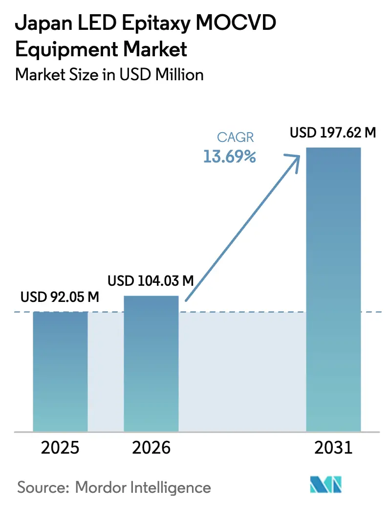
| Base Year Market Size (2025) | USD 92.05 Million |
| Market Size (2026) | USD 104.03 Million |
| Market Size (2031) | USD 197.62 Million |
| Growth Rate (2026 - 2031) | 13.69% CAGR |
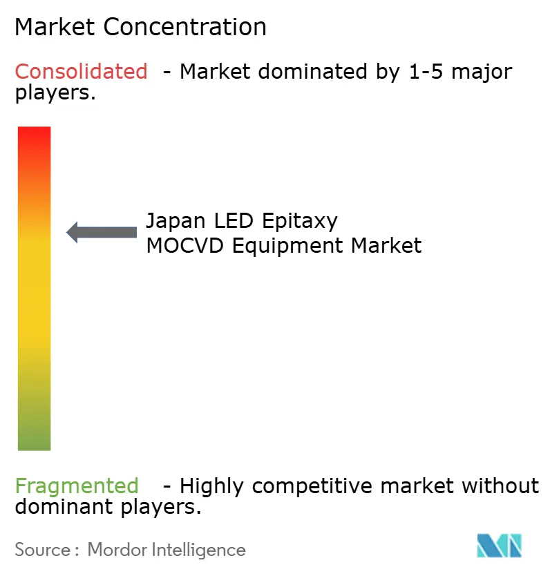
| Market Concentration | Medium |
Major Players *Disclaimer: Major Players sorted in no particular order Image © Mordor Intelligence. Reuse requires attribution under CC BY 4.0. | |
Japan LED Epitaxy MOCVD Equipment Market Analysis by Mordor Intelligence
The Japan LED epitaxy MOCVD equipment marketsize is projected to be USD 92.05 million in 2025, USD 104.03 million in 2026, and reach USD 197.62 million by 2031, growing at a CAGR of 13.69% from 2026 to 2031. An upswing in state subsidies, rapidly rising mini- and micro-LED demand, and the migration of GaN-on-Si power devices to 200 mm and 300 mm wafers underpin this expansion. Tokyo’s multi-billion-dollar fiscal‐2026 package for semiconductors signals predictable order pipelines for domestic toolmakers, while prototype breakthroughs such as a 10.2% wall-plug-efficiency UV-C LED confirm that Japan-based manufacturers are ready to scale next-generation devices. At the same time, larger wafer formats that lower die cost, and in-situ process control that shortens tool setup times, are sharpening replacement cycles for legacy reactors. Volatility in the yen does inflate imported tool costs, yet corporate net-zero mandates and energy-efficiency retrofits keep capital expenditure directed toward high-efficiency lighting and power electronics.
Key Report Takeaways
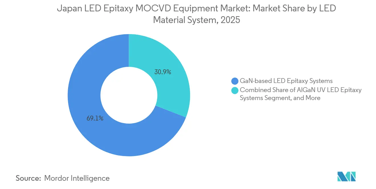
- By LED material system, GaN-based LED epitaxy systems segment held 69.09% of Japan LED epitaxy MOCVD equipment market share in 2025; AlGaN UV LED epitaxy systems segment is forecast to advance at a 14.65% CAGR through 2031.
- By wafer size capability, 150 mm segment led with 48.39% share in 2025, while 200 mm and above segment is set to grow at a 14.38% CAGR to 2031.
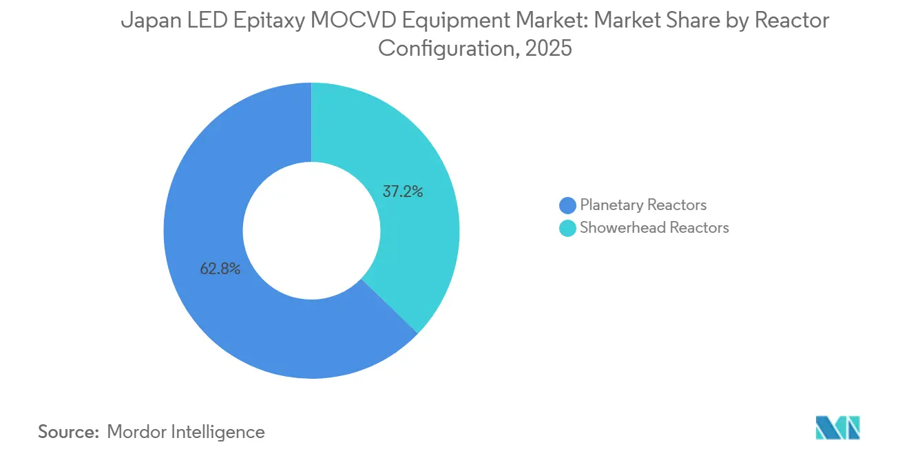
- By reactor configuration, planetary reactors accounted for 62.78% of the market share in 2025; showerhead reactors segment is projected to post the fastest 14.76% CAGR over the forecast period.
- By end user, the integrated LED manufacturer segment accounted for 72.06% of the Japan LED epitaxy MOCVD equipment market in 2025, whereas epitaxy foundries and merchant Epi suppliers segment is expanding at a 14.16% CAGR to 2031.
Note: Market size and forecast figures in this report are generated using Mordor Intelligence’s proprietary estimation framework, updated with the latest available data and insights as of January 2026.
Proportional positioning is established by comparing country level and regional contributions against the global total, including that of Japan. The led epitaxy mocvd equipment market share in our global report expresses these relative weights.
Japan LED Epitaxy MOCVD Equipment Market Trends and Insights
Drivers Impact Analysis*
| Driver | (~) % Impact on CAGR Forecast | Geographic Relevance | Impact Timeline |
|---|---|---|---|
| Surge in Mini and Micro-LED Backlighting Demand | +3.2% | Kanto and Kansai manufacturing belts | Medium term (2-4 years) |
| Government Subsidies for Domestic Semiconductor Tools | +2.8% | Nationwide, with priority in Kumamoto, Hokkaido, Hiroshima | Short term (≤ 2 years) |
| Expansion of GaN-on-Si Power Device Supply Chains | +2.5% | Nationwide, exporting to wider Asia-Pacific and North America | Medium term (2-4 years) |
| Automotive UV-C LED Adoption for In-Cabin Sterilization | +1.9% | Automotive corridors in Tokyo, Aichi, Hiroshima | Medium term (2-4 years) |
| Demand for 150 mm and 200 mm GaN Wafers from Power IC IDMs | +1.7% | Export-oriented production hubs | Long term (≥ 4 years) |
| Corporate Net-Zero Targets Accelerating High-Efficiency Lighting Retrofits | +1.5% | National roll-out driven by GX-ETS obligations | Short term (≤ 2 years) |
| Source: Mordor Intelligence | |||
Surge in Mini and Micro-LED Backlighting Demand
Mini- and micro-LED backlighting for vehicle cockpits and flagship consumer electronics has tightened epitaxy tolerances, pushing suppliers toward sub-nanometer thickness control across 150 mm and 200 mm wafers. Aixtron’s G10-AsP platform reports an order-of-magnitude reduction in defect density, aligning with Japan’s display majors that require wavelength uniformity for panels exceeding 1,000 ppi. Local R&D partnerships, including Stanley Electric and Kyoto University’s photonic-crystal surface-emitting laser program, demonstrate that domestic toolmakers can embed application-specific process recipes. Procurement cycles for these reactors average six months, rewarding vendors that pre-bundle metrology and process-transfer packages. Collectively, these developments raise per-wafer yields and shorten time-to-market for micro-LED modules, directly lifting equipment replacement demand.
Government Subsidies for Domestic Semiconductor Tools
Japan’s fiscal-2026 budget allocates JPY 1.23 trillion (USD 7.9 billion) to semiconductors and AI, quadrupling prior-year support and providing predictable, multi-year order visibility for equipment makers. Capital grants flow first to regional clusters hosting TSMC’s Kumamoto fab and Rapidus’ Hokkaido project, both of which aim for 60% domestic procurement in tool and material spend. Subsidy tranches are linked to technical milestones, lowering the risk of stranded MOCVD assets. The policy also dovetails with tightened export controls that divert Japanese supply away from restricted Chinese demand and toward on-shore or allied fabs, cushioning suppliers against geopolitical swings.
Expansion of GaN-on-Si Power Device Supply Chains
Data-center power shelves, EV onboard chargers, and fast-charging adapters are migrating to GaN-on-Si switches, accelerating adoption of 200 mm and 300 mm epitaxy. Veeco’s Propel300 reactor, ordered by a major power IDM, demonstrates defect densities compatible with 650 V devices, scaling die output by 2.3× per wafer. onsemi’s memorandum with Innoscience to sample 200 mm GaN devices in 2026 shows how fabless and fab-light models lean on specialized foundries, broadening the domestic tool addressable market. Academic validation at imec of 800 V breakdown on 300 mm QST substrates underpins confidence in further wafer-scale migration. These threads converge to lift multi-reactor orders from both IDMs and merchant foundries.
Automotive UV-C LED Adoption for In-Cabin Sterilization
Deep-UV LEDs emitting below 280 nm require high-aluminum AlGaN layers, which impose stringent gas-flow and temperature homogeneity. Taiyo Nippon Sanso’s horizontal high-flow reactor secures 0.2% AlGaN uniformity on 8-inch batches, meeting automaker reliability targets.[1]Taiyo Nippon Sanso, “Advanced High-Flow Horizontal MOCVD for Nitride,” tnsc-innovation.com ams OSRAM has reached a 10.2% wall-plug-efficiency prototype, cutting thermal management costs for in-vehicle sterilizers. Japan’s automakers, aligning with European health-safety mandates, have begun design-ins that create multi-year pull-through for UV-optimized MOCVD lines. Rising adoption in water purification skids and medical devices offers additional volume that smooths utilization rates for these reactors.
Restraints Impact Analysis*
| Restraint | (~) % Impact on CAGR Forecast | Geographic Relevance | Impact Timeline |
|---|---|---|---|
| Limited MOCVD Tool Throughput Versus SiC Epitaxy Alternatives | -1.8% | Power-device fabs benchmarking GaN against SiC | Medium term (2-4 years) |
| High Capital Intensity Amid Yen Depreciation | -2.1% | Small and mid-sized LED manufacturers nationwide | Short term (≤ 2 years) |
| Supply Chain Concentration in China for Key Components | -1.3% | Domestic integrators sourcing quartz hardware and valves | Medium term (2-4 years) |
| Slow Qualification Cycles at Japanese Automotive OEMs | -1.6% | Toyota, Honda, Nissan tier-one ecosystems | Long term (≥ 4 years) |
| Source: Mordor Intelligence | |||
Limited MOCVD Tool Throughput Versus SiC Epitaxy Alternatives
SiC CVD tools deposit thicker layers at higher rates, enabling power fabs to clear more wafers per shift than GaN MOCVD lines. Aixtron shipped its 100th G10-SiC tool in 2025, underscoring how SiC equipment can outpace GaN in high-voltage segments. Modeling studies reveal gas-phase by-product nucleation as a key bottleneck in GaN MOVPE, complicating reactor design. Consequently, several Japanese IDMs cherry-pick GaN only for sub-650 V devices, tempering total reactor demand.
High Capital Intensity Amid Yen Depreciation
The yen’s weakness inflates euro- and dollar-denominated tool prices by double-digit percentages. European reactors priced at EUR 3 million translate into higher local currency outlays, squeezing LED makers already contending with commodity gallium spikes. Some producers defer new reactors in favor of energy-saving retrofits that lower operating expense. Japan’s GX-ETS scheme introduces fresh carbon compliance costs, adding a further budget headwind.[2]Borderless Business Law Office, “2026 Energy System Changes Affecting Businesses,” borderless.law
*Our forecasts treat driver/restraint impacts as directional, not additive. The impact forecasts reflect baseline growth, mix effects, and variable interactions.
Segment Analysis
By LED Material System: GaN Sustains Leadership, UV Catalyzes Growth
The GaN-based LED epitaxy systems segment dominated the Japan LED epitaxy MOCVD equipment market, accounting for 69.09% in 2025, reflecting its entrenched role in white lighting, automotive headlamps, and display backlights. Robust process maturity, broad precursor availability, and standardized planetary reactor recipes keep GaN capital efficient, ensuring stable upgrade cycles. AlGaN UV LED epitaxy systems, while niche in 2025, are tracking a 14.65% CAGR as health-safety regulations and water disinfection projects boost volumes. Equipment buyers value showerhead reactors that curb parasitic aluminum deposition, an essential attribute for sub-280 nm emitters. Concurrently, research into strain-relaxed bulk InGaN aims to displace AlInGaP in red pixels, which would further consolidate spend around GaN family chemistries.
The Japan LED epitaxy MOCVD equipment market share for GaN is also protected by domestic integration moves such as ROHM’s plan to bring TSMC GaN recipes in-house. Yet UV suppliers confront higher precursor costs and stricter contamination control, raising barriers for new entrants. Long-term, cross-platform hybrid lines combining MOCVD for active layers with HVPE for thick buffers could cut per-wafer cost, but current pilot results remain limited to 4-inch experiments.


By Wafer Size Capability: Migration Toward 200 mm and 300 mm Platforms
Tools configured for 150 mm wafers held 48.39% of the Japan LED epitaxy MOCVD equipment market share in 2025 because legacy GaN-on-sapphire and GaN-on-Si lines remain profitable at mid-volumes. However, 200 mm and larger systems are registering a 14.38% CAGR as IDMs chase lower die cost and foundries monetize scale economics. The Propel300’s qualification for automotive-grade 650 V GaN validates defectivity levels acceptable for power modules, signaling that mass adoption of 300 mm epitaxy is plausible this decade. Pilot programs at academic consortia such as imec further de-risk this transition by publishing >800 V breakdown data on 300 mm QST substrates.
The scale shift is not friction-free. Free-standing GaN substrates above 6 inches remain scarce, compelling many LED makers to stay on 150 mm GaN-on-sapphire. Process migration also involves six-month stabilization windows, during which yield drag can offset wafer-cost gains. Even so, Japan’s tool vendors increasingly bundle automated wafer handling and AI-driven run-to-run control that shorten this learning curve.
By Reactor Configuration: Planetary Dominance Faces Uniformity-Driven Challenge
Planetary reactors captured 62.78% of the market share in 2025 thanks to multi-wafer throughput, horizontal laminar flow, and proven uniformity for mainstream blue and white GaN. Close-coupled showerhead reactors, however, is set to post a 14.76% CAGR by 2031 as micro-LED and UV applications demand tighter indium and aluminum uniformity across larger wafers. Computational modeling highlights gas flow, showerhead gap, and inlet temperature as critical variables for showerhead yield optimization.[3]Zhi Zhang, Haisheng Fang, Han Yan, Zhimin Jiang, Jiang Zheng, and Zhiyin Gan, “Influencing Factors of GaN Growth Uniformity Through Orthogonal Test Analysis,” Applied Thermal Engineering, sciencedirect.com
Planetary incumbents are not standing still. Trials of triple-flow gas injectors achieved 0.16% AlGaAs growth-rate uniformity on 6-inch batches, suggesting that planetary tools can still meet next-generation specs with targeted upgrades. Buyers thus weigh uniformity gains against throughput trade-offs, often opting for mixed fleets where showerhead tools handle premium micro-LED and UV runs while planetary reactors process volume blue-LED lots.
By End User: Foundry Share Rises Amid Capital Discipline
Integrated manufacturers owned 72.06% of Japan LED epitaxy MOCVD equipment market share in 2025, a legacy of vertical integration where firms protect process IP. Yet epi-foundries are growing at a 14.16% CAGR as fab-light power-device designers and specialty LED houses outsource wafer production. Partnerships such as onsemi-Innoscience showcase this pivot, letting device makers scale without USD 30 million in upfront reactor outlays. Licensing deals, including Polar Semiconductor’s adoption of Renesas GaN IP, further confirm a shift toward distributed manufacturing.
OEMs in automotive lighting require dual sourcing, which compels many integrated players to maintain captive capacity for strategic wavelengths or safety-critical parts. This approach leads to a hybrid procurement model that combines internal production lines with external foundries. As a result, it helps stabilize demand for both new tool purchases and contract epitaxy slots.
Geography Analysis
Japan’s geography-driven cluster strategy concentrates advanced epitaxy capabilities across three corridors. Kyushu hosts the Kumamoto logic hub where TSMC’s 3 nm expansion stimulates local chemical, wafer, and tool supply. Hokkaido’s Chitose cluster, anchored by Rapidus, is earmarked for 2 nm R&D and compound pilot lines, distributing demand away from seismic-risk regions in central Honshu. The Kansai corridor remains pivotal for automotive lighting, laser diodes, and UV-LEDs, thanks to proximity to Toyota and Honda Tier 1 suppliers.
Government policy cements these nodes through land grants, tax offsets, and power-grid upgrades, raising the Japan LED epitaxy MOCVD equipment market outlook. Subsidy design stipulates percentage thresholds for domestic procurement, channeling orders toward Japanese reactor makers and gas suppliers. Academic–industry linkage adds another geographic pull: national universities in Sendai, Nagoya, and Fukuoka operate open-access cleanrooms that vet prototype reactors, accelerating local vendor qualification.
Geopolitical factors also shape spatial demand. Export-control alignment with the United States diverts potential China-bound tool volumes back into domestic fabs or trusted‐partner destinations such as Southeast Asia. Meanwhile, raw-material security measures, like JX Nippon Mining’s 20% InP substrate capacity hike in Ibaraki, localize critical precursor supply. Collectively, these dynamics widen regional order books for both 150 mm retrofit tools and 200 mm green-field lines.
Mordor Intelligence examines the led epitaxy mocvd equipment market across diverse other regional markets as well, including Asia, while also offering granular country-level perspectives for Taiwan and China and more.
Competitive Landscape
European incumbents Aixtron and Veeco remain the benchmark suppliers in Japan LED epitaxy MOCVD equipment market contracts, but domestic challenger Taiyo Nippon Sanso is closing the gap by packaging reactors with proprietary gas panels and on-site abatement. Aixtron’s G-series backlog surpassed EUR 280 million in late 2025, buoyed by demand for multi-material flexibility across GaN, AsP, and SiC. Veeco secured Propel300 wins at a Japanese power IDM, signaling early‐mover advantage in the 300 mm transition.
Taiyo Nippon Sanso differentiates on AlGaN uniformity, recording 0.2% composition variation on 8-inch wafers during pilot UV runs. The firm’s new European distributor network points to expansion beyond its historic gas-supply stronghold into full-tool exports. Strategic co-development between equipment vendors and device makers further raises switching costs; for instance, Stanley Electric’s PCSEL R&D with Kyoto University implicitly locks in specific reactor chemistries.
Rising Chinese OEMs, especially in SiC and GaN tools, remain a long-term wildcard. Although export restrictions temper their immediate presence in Japan, their rapid domestic scaling could erode price premiums enjoyed by incumbents. To defend margins, established suppliers are embedding AI-driven run-to-run control and predictive maintenance features that reduce lifetime cost of ownership, reinforcing value differentiation beyond basic deposition capability.
Japan LED Epitaxy MOCVD Equipment Industry Leaders
Aixtron SE
Veeco Instruments Inc.
Advanced Micro-Fabrication Equipment Inc. China
Taiyo Nippon Sanso Corporation
Tokyo Electron Limited
- *Disclaimer: Major Players sorted in no particular order

Recent Industry Developments
- March 2026: Veeco Instruments booked multiple Lumina MOCVD and Spector ion-beam systems from a leading optical-communications laser maker, cementing Lumina as the customer’s production workhorse.
- February 2026: ROHM initiated TSMC GaN process transfer to its Hamamatsu fab, targeting end-to-end GaN production readiness by 2027.
- January 2026: Kanematsu GmbH began distributing Taiyo Nippon Sanso MOCVD tools in Europe, shipping systems to Lund University and the Polish Institute of High Pressure Physics.
- December 2025: onsemi and Innoscience signed a memorandum to co-expand 200 mm GaN power-device production, eyeing first samples in H1 2026.


Japan LED Epitaxy MOCVD Equipment Market Report Scope
The LED Epitaxy MOCVD Equipment Market refers to the segment of the semiconductor equipment industry focused on manufacturing Metal-Organic Chemical Vapor Deposition (MOCVD) systems used for the epitaxial growth of LED materials. These systems are critical for producing high-quality LED wafers, which serve as the foundation for LED devices used in various applications such as lighting, displays, and automotive technologies.
The Japan LED Epitaxy MOCVD Equipment Market Report is Segmented by LED Material System (GaN-based LED Epitaxy Systems, AlGaN UV LED Epitaxy Systems, and AlInGaP LED Epitaxy Systems), Wafer Size Capability (Up to 100mm, 150mm, and 200mm and Above), Reactor Configuration (Planetary Reactors, and Showerhead Reactors), and End User (Integrated LED Manufacturers, and Epitaxy Foundries and Merchant Epi Suppliers). The Market Forecasts are Provided in Terms of Value (USD).
| GaN-based LED Epitaxy Systems |
| AlGaN UV LED Epitaxy Systems |
| AlInGaP LED Epitaxy Systems |
| Upto 100 mm |
| 150 mm |
| 200 mm and Above |
| Planetary Reactors |
| Showerhead Reactors |
| Integrated LED Manufacturers (IDMs) |
| Epitaxy Foundries and Merchant Epi Suppliers |
| By LED Material System | GaN-based LED Epitaxy Systems |
| AlGaN UV LED Epitaxy Systems | |
| AlInGaP LED Epitaxy Systems | |
| By Wafer Size Capability | Upto 100 mm |
| 150 mm | |
| 200 mm and Above | |
| By Reactor Configuration | Planetary Reactors |
| Showerhead Reactors | |
| By End User | Integrated LED Manufacturers (IDMs) |
| Epitaxy Foundries and Merchant Epi Suppliers |


Key Questions Answered in the Report
How fast is Japan’s LED epitaxy MOCVD equipment market growing?
It is forecast to register a 13.69% CAGR from 2026 to 2031, rising from USD 104.03 million in 2026 to USD 197.62 million by the end of the period.
Which LED material system leads current tool demand?
GaN-based reactors dominate, holding 69.09% share in 2025 thanks to solid-state lighting, automotive headlamps, and display backlighting orders.
Why are 200 mm and 300 mm wafers important for Japanese suppliers?
Larger wafers lower die cost and, with tools such as Propel300, deliver up to 2.3× more chips per run, boosting capacity without proportional floor-space increases.
What policy factors support domestic toolmakers?
Japan’s fiscal-2026 budget allocates USD 7.9 billion to semiconductors, with grants tied to local procurement percentages that favor domestic MOCVD vendors.
How do showerhead reactors differ from planetary designs?
Showerhead tools inject precursors vertically and very close to the wafer, cutting gas-phase reactions and improving uniformity for high-indium or high-aluminum layers, though they process fewer wafers per batch than planetary systems.
Which restraint currently weighs most on market growth?
Yen depreciation raises the local cost of euro- and dollar-priced reactors, especially for small and mid-sized LED manufacturers, trimming near-term capital budgets.
Page last updated on:


