
Size and Share of Solder Materials Market In Semiconductor Industry
Market Overview
| Study Period | 2021 - 2032 |
|---|---|
| Market Size (2027) | USD 1.11 Billion |
| Market Size (2032) | USD 1.56 Billion |
| Growth Rate (2027 - 2032) | 7.04 % |
| Fastest Growing Market | Asia-Pacific |
| Largest Market | Asia-Pacific |
| Market Concentration | Medium |
Major Players *Disclaimer: Major Players sorted in no particular order Image © Mordor Intelligence. Reuse requires attribution under CC BY 4.0. | |
Analysis of Solder Materials Market In Semiconductor Industry by Mordor Intelligence
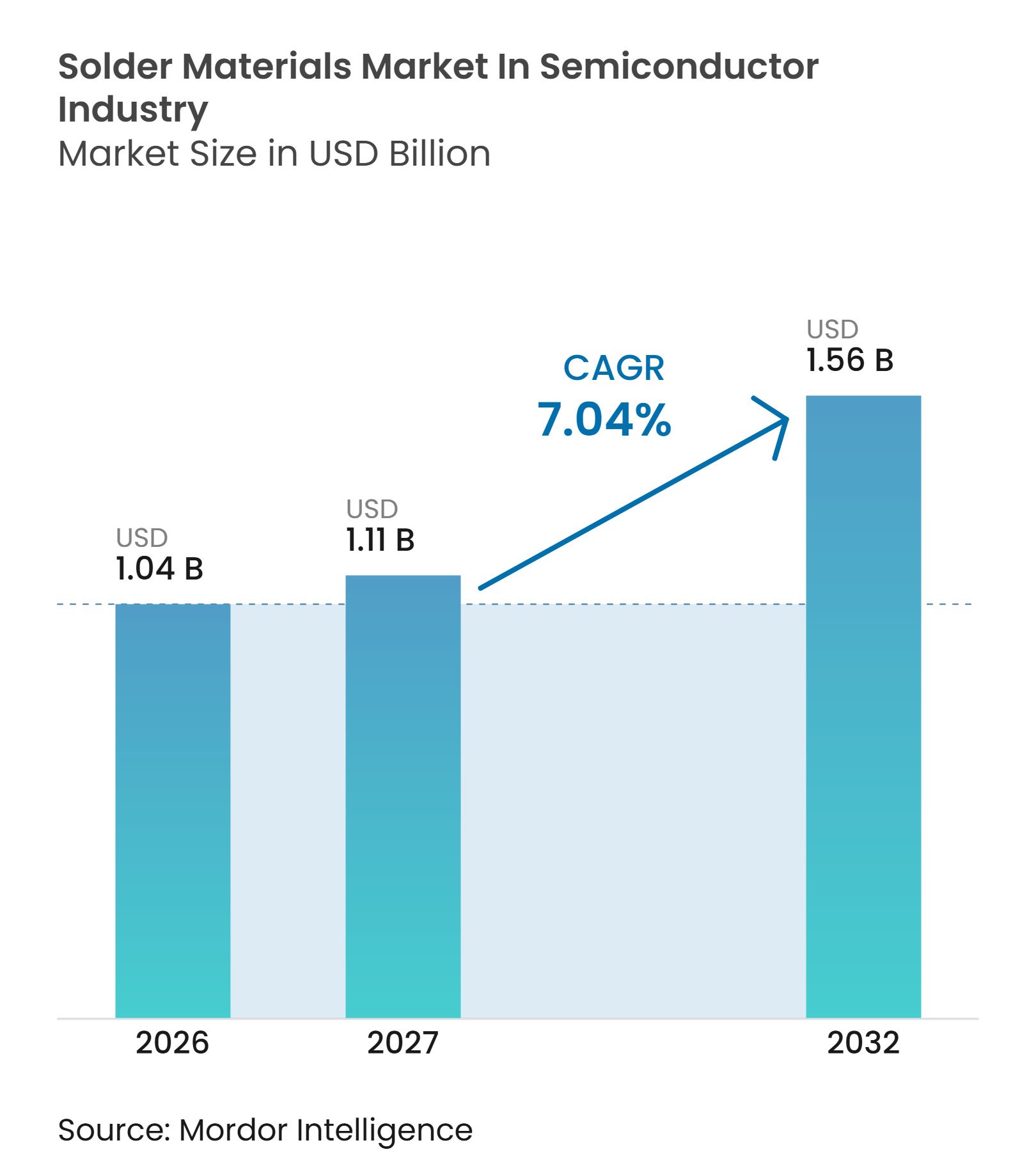
The solder materials market in semiconductor industry size is valued at USD 1.04 billion in 2026 and is forecast to reach USD 1.56 billion by 2032, expanding at a CAGR of 7.04% from 2027 to 2032. Advanced packaging is moving more semiconductor value into the back end, where solder remains necessary for flip-chip bumping, BGA ball attach, wafer-level bump formation, and die attach. AI accelerators and high-bandwidth memory are increasing the number and density of interconnects within each package. The shift raises material demand per device, rather than only increasing unit shipments. Lead-free requirements are also widening the range of alloys that suppliers must support. Direct copper bonding will affect the finest-pitch connections over time, but solder continues to serve several package interfaces.
Key Report Takeaways
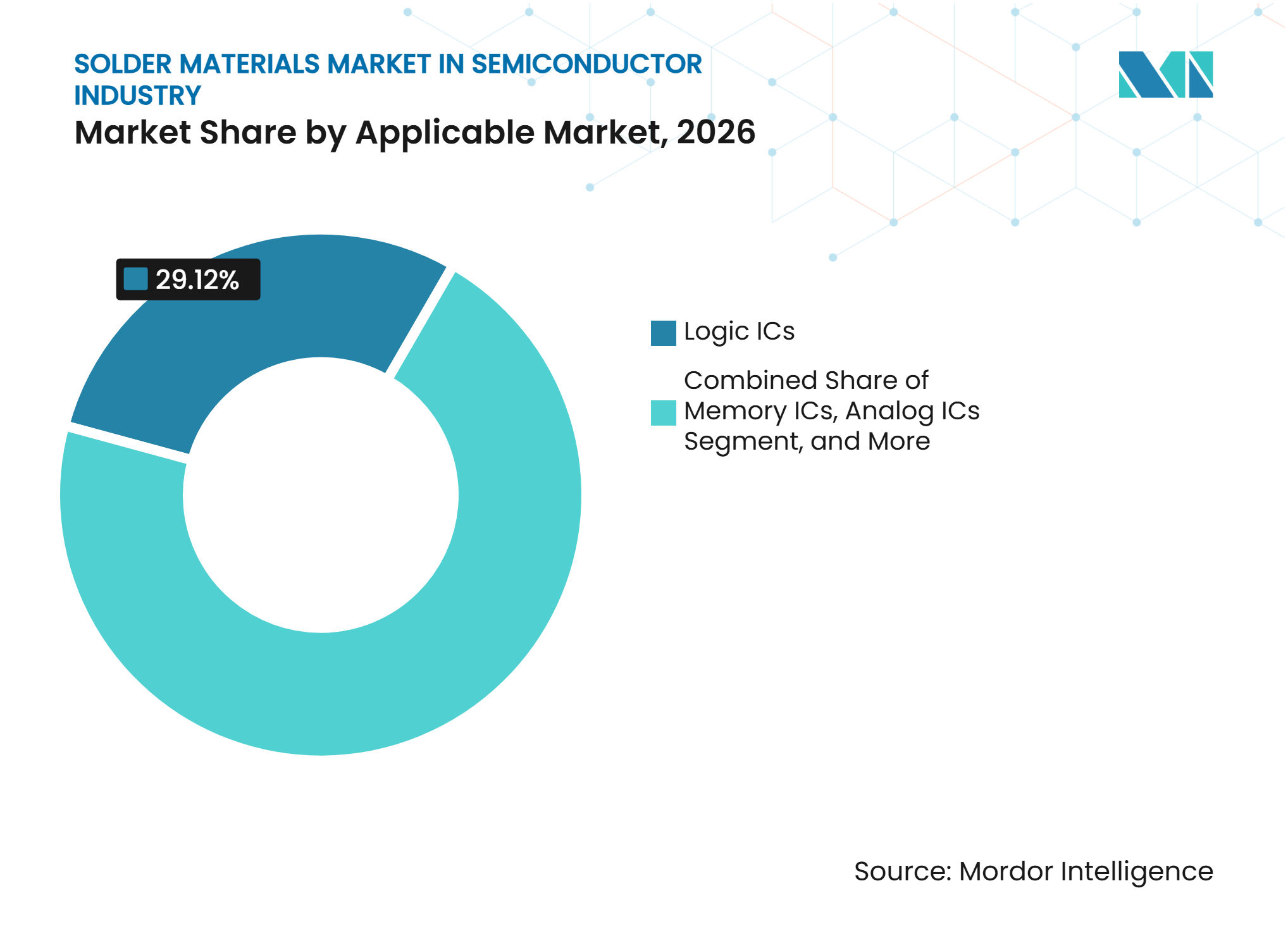
- By applicable market, Logic ICs held 29.12% of the solder materials market in semiconductor industry market share in 2026, while Memory ICs are projected to expand at a 7.44% CAGR through 2032.
- By product form, solder paste accounted for 31.92% of the market in 2026, while solder balls and spheres are projected to expand at a 7.38% CAGR through 2032.
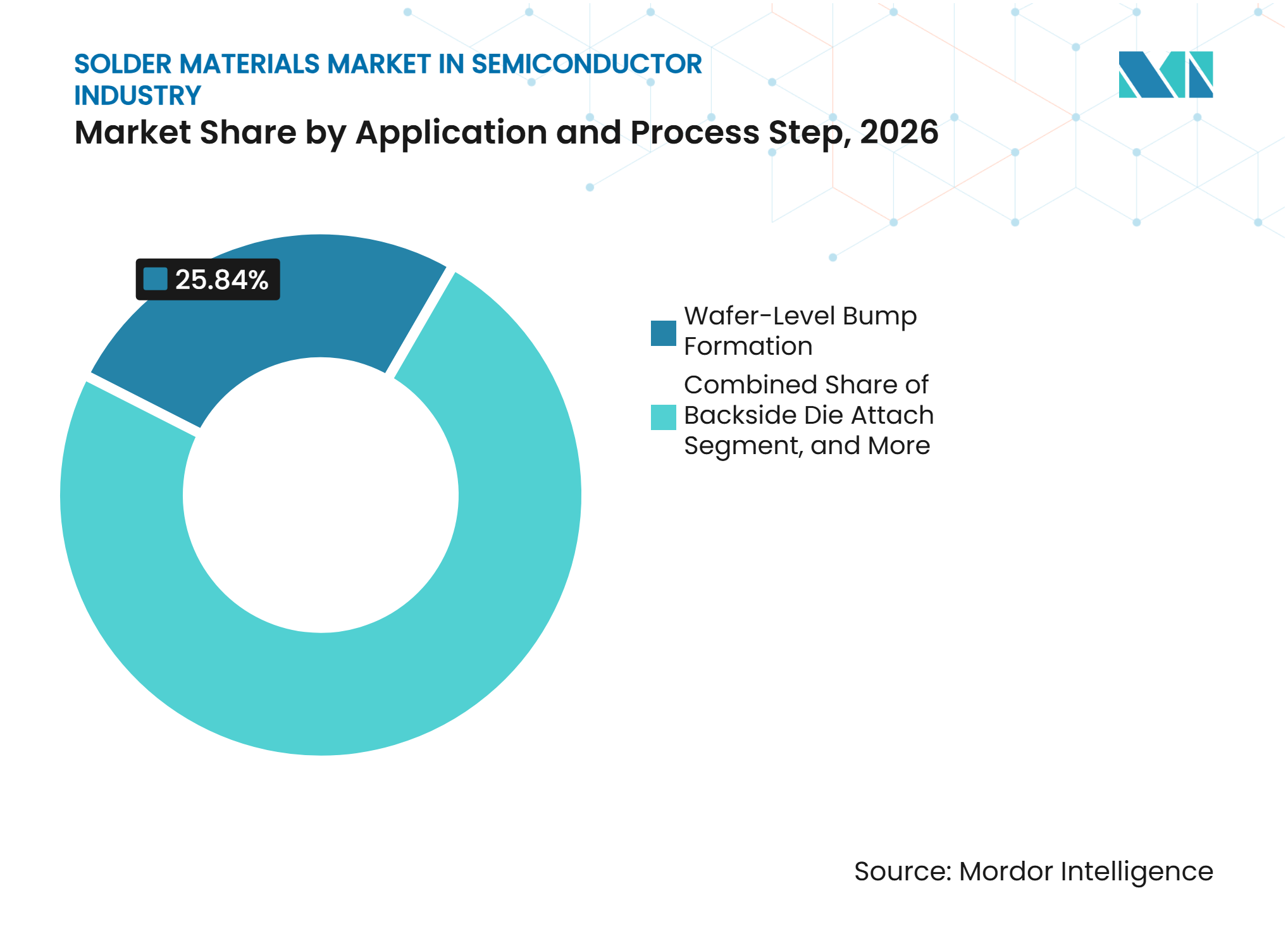
- By application and process step, wafer-level bump formation held 25.84% of the market in 2026 and is projected to expand at a 7.31% CAGR through 2032.
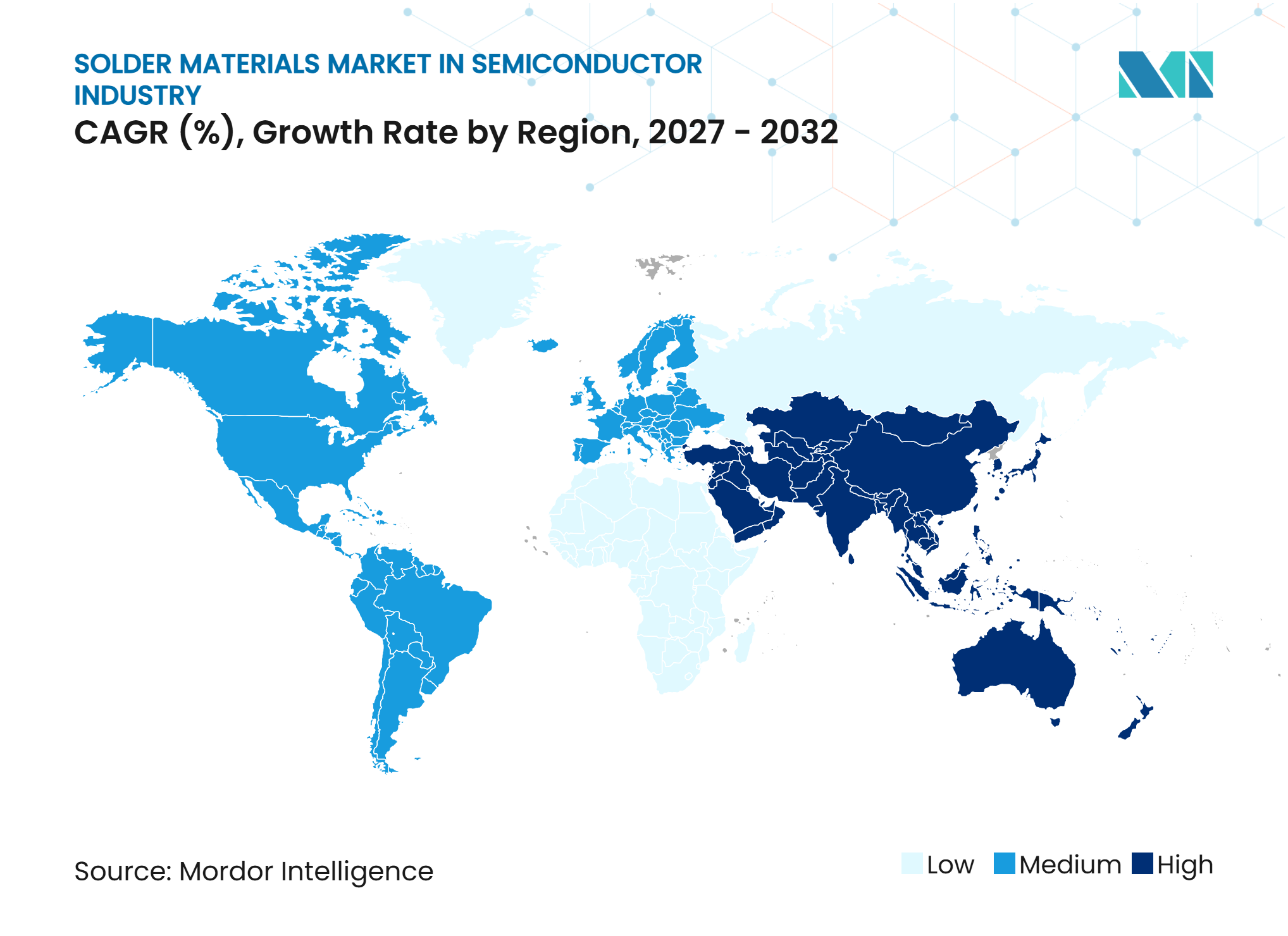
- By geography, Asia-Pacific held 59.98% of the solder materials market in semiconductor industry market share in 2026 and is projected to expand at a 7.46% CAGR through 2032.
Note: Market numbers in this report are based on Mordor Intelligence's proprietary estimation framework, which combines nine months of actuals with Q4 projections for base year 2026.
Market Trends and Insights
Drivers Impact Analysis of Solder Materials Market In Semiconductor Industry*
| Driver | (~) % Impact on CAGR Forecast | Geographic Relevance | Impact Timeline |
|---|---|---|---|
| AI-Driven Advanced Packaging and HBM Demand | +2.1% | Global, led by Taiwan, South Korea, and North America | Short term (≤ 2 years) |
| Growth of Heterogeneous Integration and 2.5D/3D Packaging | +1.6% | Asia-Pacific core, spillover to North America and Europe | Medium term (2-4 years) |
| Adoption of Fan-Out Wafer-Level and Panel-Level Packaging | +1.1% | Asia-Pacific core, especially Taiwan and China, expanding to North America | Medium term (2-4 years) |
| Electronics Miniaturization and Ultra-Fine Solder Paste Demand | +0.9% | Global, concentrated in Japan, Taiwan, and South Korea | Short term (≤ 2 years) |
| Lead-Free Material Transition | +0.7% | Global, with strongest compliance pressure in Europe and North America | Long term (≥ 4 years) |
| Vertical Integration of Advanced Packaging by Foundries | +0.5% | Global, led by Taiwan, North America, and South Korea | Medium term (2-4 years) |
| Source: Mordor Intelligence | |||
AI-Driven Advanced Packaging and HBM Demand
Generative AI, cloud inference, and data center investment are raising packaging density and solder use in HBM stacks, interposers, and AI modules. The solder materials market in semiconductor industry benefits because an accelerator package can combine a logic die with several memory stacks. Fine-pitch microbumps remain a practical attachment approach for current HBM generations. The IEEE Heterogeneous Integration Roadmap reports that advanced multi-chip packages commonly contain several dozen dies, increasing the need for precise interconnect deposition and attachment processes.[1] More dies and higher memory counts increase the interconnect requirement in each completed package. This supports demand even when chip shipment growth is slower than the rise in package complexity.
Growth of Heterogeneous Integration and 2.5D/3D Packaging
Heterogeneous integration combines dies made on different process nodes in one package, which increases the role of interconnect materials. Solder microbumps remain important at chip-to-substrate interfaces even when direct bonding is used between selected dies. An IEEE ECTC 2025 study found that low-melting-temperature solder reduced warpage to less than 200 µm in a 120 mm by 120 mm 2.5D test vehicle at reflow temperatures from 160 °C to 200 °C.[2] This result is relevant as AI packages become larger and more difficult to mount reliably. Larger interposers can also increase solder ball counts before HBM connections are included. The solder materials market in semiconductor industry therefore has exposure to higher material content per package as chiplet designs become more complex.
Adoption of Fan-Out Wafer-Level and Panel-Level Packaging
Fan-out wafer-level packaging and fan-out panel-level packaging use redistribution layers and require reliable bumping and package-to-board attachment. These platforms create demand for solder materials at several stages rather than at a single interface. High-density fan-out designs for AI systems can use embedded bridges that require fine-pitch connections between the bridge and die. Panel-level processing also changes stencil-printing conditions because the panel format is larger than a round wafer. This creates a need for paste formulations with stable rheology and controlled deposition. The solder materials market in semiconductor industry can benefit when qualified formulations move from development to volume production.
Electronics Miniaturization and Ultra-Fine Solder Paste Demand
Smaller components and finer assembly pitches are increasing demand for ultra-fine solder paste. AI edge devices, 5G modules, and system-in-package products require precise printing with low bridging and limited voiding. Indium Corporation introduced Indium12.9HF in 2026 for sub-175 µm pad printing and BGA, CSP, LGA, and QFN applications.[3] Fine-powder processing and production support are becoming important product differentiators. Qualification effort also makes it harder for customers to replace a proven paste formulation. The solder materials market in semiconductor industry is therefore moving beyond standard paste toward application-specific materials for tighter process windows.
Restraints Impact Analysis of Solder Materials Market In Semiconductor Industry*
| Restraint | (~) % Impact on CAGR Forecast | Geographic Relevance | Impact Timeline |
|---|---|---|---|
| Substitution by Cu-Cu Hybrid Bonding | -1.4% | Global, led by Taiwan, South Korea, and North America | Long term (≥ 4 years) |
| Complex Solder Alloy Qualification Requirements | -0.9% | Global, with strongest compliance influence in Japan, Europe, and North America | Medium term (2-4 years) |
| Customer Concentration and Supplier Pricing Pressure | -0.7% | Global, most acute in Taiwan, South Korea, and China | Short term (≤ 2 years) |
| Raw Material Supply Chain Concentration Risks | -0.6% | Global, with critical exposure in indium, tin, and bismuth sourcing | Medium term (2-4 years) |
| Source: Mordor Intelligence | |||
Substitution by Cu-Cu Hybrid Bonding
Copper-to-copper hybrid bonding can replace solder microbumps at the finest die-to-die pitches. It is being used for selected logic and cache stacking applications, which creates a long-term substitution risk. Applied Materials identifies hybrid bonding as a critical process for chiplet-to-wafer integration, where alignment and surface preparation are central requirements. The technology does not remove the need for solder at chip-to-substrate and package-to-board interfaces. Those interfaces remain material-intensive parts of advanced packages. The restraint is therefore focused on a narrow but technologically important part of the solder materials market in semiconductor industry.
Complex Solder Alloy Qualification Requirements
New solder alloys require extended testing for solderability, thermal cycling, moisture sensitivity, and customer-specific reliability conditions. IPC J-STD-006, ISO 9453, and IEC 61190 shape this process, while customer approval can extend across several production cycles. The DA5 consortium reviewed more than 218 candidate materials from more than 18 suppliers, and more than 50 materials received extensive testing. As of July 2026, the work had not identified a universal replacement for high-melting-temperature lead solders across semiconductor packaging applications. The qualification burden requires suppliers to keep existing materials available while validating alternatives. This can delay material changes and increase the cost of bringing a new chemistry into the solder materials market in semiconductor industry.
*Our forecasts treat driver/restraint impacts as directional, not additive. The impact forecasts reflect baseline growth, mix effects, and variable interactions.
Solder Materials Market In Semiconductor Industry Segment Analysis
By Applicable Market:
Logic ICs Hold the Largest Position While Memory ICs AccelerateLogic ICs held 29.12% of the solder materials market in semiconductor industry market size in 2026, while Memory ICs are projected to expand at a 7.44% CAGR from 2027 to 2032. Logic packages use large flip-chip bump arrays in AI processors, network switching ASICs, graphics processors, and high-performance CPUs. These devices often use 2.5D interposer architectures with multiple memory stacks. A CoWoS-L package can combine a logic die with 6 to 8 HBM stacks, which raises solder content per completed device. This supports Logic IC revenue even as package designs shift toward disaggregated chiplets. The segment’s position rests on both device volumes and higher packaging intensity.
Memory ICs are supported by the HBM roadmap and by LPDDR5X and next-generation DRAM in AI edge and mobile products. Thermo-compression microbump attachment remains relevant to current stacked-memory assembly. Indium Corporation’s 2026 collaborative work on SnBi interconnects found a warpage reduction of more than 70 µm compared with SAC305 reflow conditions, while maintaining comparable thermal aging and shock resistance. Compound semiconductors and power devices require specified alloys and die-attach geometries for automotive and power applications. Analog ICs, sensors, MEMS, RF products, and optical devices add specialized demand where voiding control and attachment precision matter. These requirements broaden the solder materials market in semiconductor industry beyond standard SAC and SnPb formulations.


By Product Form:
Paste Retains Breadth While Solder Balls and Spheres Expand FasterSolder paste accounted for 31.92% of the solder materials market size in 2026, while solder balls and spheres are projected to expand at a 7.38% CAGR through 2032. Paste is used in stencil printing, BGA re-balling, wafer-level bump formation, die attach, and package sealing. Its broad application across device types and assembly steps supports its leading position. Semiconductor packaging material consumption was projected by SEMI to rise 8% in 2025 to USD 5.4 billion and a further 15% in 2026. This wider materials demand supports paste volumes across conventional and advanced assembly.
Solder balls and spheres benefit from HBM stacking, BGA AI accelerator packages, and server systems that use several HBM modules per socket. Their quality requirements include controlled composition, diameter precision, and low voiding. Heraeus Electronics introduced Welco AP520 Type 7 paste in 2025 for thin, complex substrates where voiding and cold-joint risks require tighter powder and process control. Preforms serve high-reliability die attach and sealing tasks in power, RF, and defense components. Wire and flux continue to support rework, robotic soldering, and mixed-assembly production. Powder remains important to the solder materials market in semiconductor industry because specialty producers use it for faster paste customization.
By Application and Process Step:
Wafer-Level Bump Formation Leads Both MeasuresWafer-level bump formation held 25.84% of the solder materials market size in 2026 and is projected to expand at a 7.31% CAGR from 2027 to 2032. The process supports flip-chip bump deposition for logic devices, AI accelerators, and memory products. It requires high consistency in solder volume, placement, and alloy composition. Its leading share and fastest projected expansion reflect the central role of bumping in advanced packaging. Foundries and outsourced semiconductor assembly and test providers are adding capacity for these processes. The result is a durable need for tightly controlled solder inputs.
Package-to-board attachment through BGA and CSP ball attach also benefits from higher AI server content. Large accelerator boards use several package types that require controlled-composition solder spheres. A 2025 study in Electronic Materials found that reducing microbump pitch from 85 µm to 5 µm reduced fatigue life by more than 73.7% across standard solder materials. The finding reinforces the need to match alloy and geometry at fine pitches. Die-to-substrate interconnection is moving toward finer copper-pillar and solder-cap structures as chiplet I/O counts rise. This maintains technical demand in the solder materials market in semiconductor industry for controlled solder inputs.

Geography Analysis
Asia-Pacific
Asia-Pacific held 59.98% of regional demand in 2026 and is projected to expand at a 7.46% CAGR through 2032. Taiwan, South Korea, Japan, and China contain a dense base of fabrication, packaging, test, and materials operations. The region has strong demand from AI chiplets and stacked memory production. Japan also supplies specialized solder products and materials to other assembly centers in the region. India is emerging as a semiconductor packaging location, creating a longer-term local opportunity for materials suppliers. Indium Corporation and TANAKA Precious Metals have identified the need for materials suited to advanced packaging and high-reliability attachment.
North America
North America is adding domestic advanced packaging and test capability, which is creating new demand for qualified solder materials. The region has a concentration of AI computing, compound semiconductors, power devices, and defense electronics. These end uses require high-temperature die attach, hermetic sealing, and controlled attachment processes. AI data center investment also supports optical transceiver and power-module demand. Indium Corporation’s 2026 product program for advanced packaging included fine-pitch flip-chip materials, low-temperature alloys for warpage-sensitive applications, and solder thermal interface materials. These requirements make North America a distinct demand center for the solder materials market in semiconductor industry.
Europe, South America, Middle East and Africa, and the Rest of Asia-Pacific
Europe’s solder materials demand is tied to automotive electronics, power modules, and compound semiconductor applications. RoHS compliance is an important regulatory influence because the European Commission’s Delegated Directive (EU) 2025/1802 restructures high-melting-temperature lead-solder exemptions into seven sub-entries that expire on December 31, 2027. South America and Middle East and Africa remain smaller assembly-led demand areas where standard SAC alloys are more prevalent. Vietnam, the Philippines, and Malaysia are becoming more relevant as packaging operations diversify within Asia-Pacific. Malaysia-based precision sphere suppliers support memory and consumer IC packaging needs. Across these mixed geographies, low-cost assembly demand coexists with specialized requirements for automotive, RF, power, and optical devices. The solder materials market in semiconductor industry will depend on suppliers matching local cost needs with the qualification standards of higher-value applications.
Competitive Landscape
Market Concentration
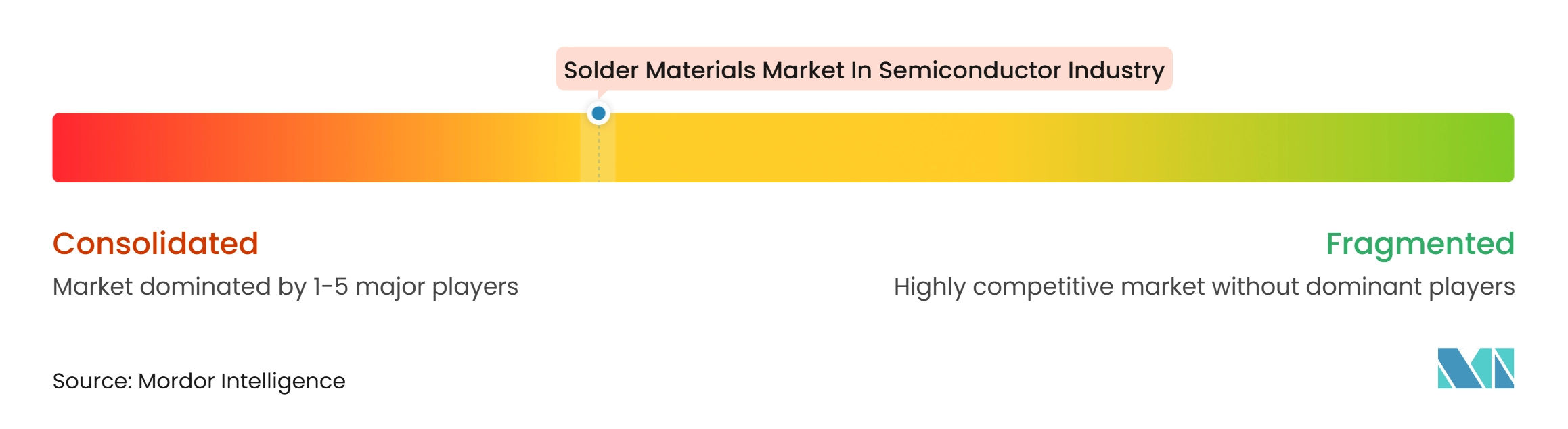
The solder materials market in semiconductor industry has a moderately concentrated upper tier and a wider group of regional suppliers. MacDermid Alpha Electronics Solutions, Indium Corporation, Heraeus Electronics, and Henkel serve advanced packaging customers with alloy portfolios and application engineering support. Their competitive position depends on formulation performance, fine-powder processing, reliability data, and support near customer production sites. Heraeus Electronics, MacDermid Alpha Electronics Solutions, and Henkel obtained a favorable outcome in the German patent dispute over the Innolot lead-free alloy in February 2025. The decision shows that intellectual property remains important in high-reliability lead-free formulations.
Product development in the solder materials market in semiconductor industry focuses on thermal control, low voiding, warpage management, and reliability at finer pitches. TANAKA Precious Metals disclosed an AgSn transient liquid phase bonding sheet in 2025 with a reported 3,000 thermal cycles and bond strength of up to 50 MPa. Henkel launched LOCTITE ABLESTIK CDF900 in August 2026, a conductive die attach film with thermal conductivity above 8 W/(m·K) for high-density packaging uses. MacDermid Alpha Electronics Solutions also highlighted sintered silver products and TrueHeight solder preforms for power electronics at PCIM Europe 2026. These actions show competition across both conventional solder and adjacent bonding materials.
Regional suppliers retain positions where local service, customer relationships, and specialized sphere production are decisive. DUKSAN Hi-Metal and MK Electron focus on high-purity solder balls for memory packaging in South Korea. Shenmao Technology has presented low-temperature solder ball uses for advanced packaging, while Nippon Micrometal serves precision sphere applications. Foundries and large outsourced semiconductor assembly and test companies are increasing direct qualification work with materials vendors. This increases pressure on mid-tier suppliers that lack deep application engineering resources. Fan-out panel-level packaging and solder thermal interface materials remain areas where technical gaps can create openings in the solder materials market in semiconductor industry. The market concentration score is 6 because the leading global suppliers have a strong position in advanced packaging, while regional companies retain meaningful positions across local and specialized applications.
Leaders of Solder Materials Market In Semiconductor Industry
-
Henkel AG & Co. KGaA
-
Indium Corporation
-
MacDermid Alpha Electronics Solutions
-
Senju Metal Industry Co., Ltd.
-
Heraeus Electronics
- *Disclaimer: Major Players sorted in no particular order
Solder Materials Market In Semiconductor Industry Companies Covered in this Report
- Indium Corporation
- MacDermid Alpha Electronics Solutions
- Henkel AG & Co. KGaA
- Senju Metal Industry Co., Ltd.
- Tamura Corporation
- Heraeus Electronics
- Nihon Superior Co., Ltd.
- KOKI Company Limited
- AIM Solder
- Qualitek International, Inc.
- Nihon Genma Mfg. Co., Ltd.
- Nihon Handa Co., Ltd.
- Kester
- DUKSAN Hi-Metal Co., Ltd.
- Shenmao Technology, Inc.
- MK Electron Co., Ltd.
- Nippon Micrometal Corporation
- MI Technovation Berhad, Accurus Scientific
- TANAKA Precious Metals
- Materion Corporation
- PFARR Stanztechnik GmbH
Recent Industry Developments in Solder Materials Market In Semiconductor Industry
- October 2026: Indium Corporation presented 5 technical papers at SMTA International 2026 in Rosemont, Illinois, covering thermal interface materials, defect mitigation, and lead-free assembly protocols for advanced semiconductor packaging, reinforcing its positioning as a specialist in AI-enabling solder and bonding materials ahead of the 2027 lead-free compliance cycle.
- September 2026: Indium Corporation showcased AI-enabling solder and thermal interface solutions at SEMICON Taiwan 2026, highlighting production-ready fine-pitch microbump flip-chip materials, WS-641, patented Durafuse® LT for warpage-critical fine-pitch applications, and reflowed solder TIM solutions designed to address voiding and thermal management in high-power AI packages.
- September 2026: Indium Corporation participated in EFX 2026 in Stuttgart, Germany, showcasing Durafuse® HR for automotive thermal cycling reliability applications and Indium12.9HF halogen-free solder paste for 01005 and 008004 component printing.
- August 2026: Henkel Adhesive Technologies launched LOCTITE ABLESTIK CDF900, a next-generation conductive die attach film with thermal conductivity exceeding 8 W/(m·K), at SEMICON Taiwan 2026, targeting AI, 5G/6G, and high-performance computing packaging applications where rising thermal density challenges conventional die attach materials.
Scope of Report on Solder Materials Market In Semiconductor Industry
The Solder Materials Market in Semiconductor Industry Market encompasses the production and supply of specialized solder materials used in semiconductor assembly, packaging, and interconnection processes. These materials enable reliable electrical connections, thermal management, and mechanical bonding between semiconductor dies, substrates, and electronic components. The market covers solder-based solutions supporting advanced packaging technologies, high-density interconnections, and miniaturized semiconductor devices. Growing demand for high-performance chips, increasing semiconductor packaging complexity, and advancements in electronic manufacturing technologies drive the adoption of solder materials across the global semiconductor industry.
The Solder Materials Market in Semiconductor Industry Report is Segmented by Applicable Market (Logic ICs, Memory ICs, Compound Semiconductors and Power Devices, Analog ICs, Sensors, MEMS and RF Devices, and Optical and Photonic Devices), Product Form (Solder Paste, Solder Balls and Spheres, Solder Preforms, Solder Wire, Solder Fluxes, Standalone, and Solder Powder, Externally Sold), Application and Process Step(Wafer-Level Bump Formation, Die-to-Substrate Interconnection, Conventional Flip-Chip, Package-to-Board Interconnection, BGA and CSP Ball Attach, Backside Die Attach, and Package Sealing and Component Attachment), and Geography (North America, South America, Europe, Asia-Pacific, Middle East, Africa). The Market Forecasts are Provided in Terms of Value (USD). The Market Forecasts are Provided in Terms of Value (USD).
Segmentation Overview
| Logic ICs |
| Memory ICs |
| Compound Semiconductors and Power Devices |
| Analog ICs |
| Sensors, MEMS and RF Devices |
| Optical and Photonic Devices |
| Solder Paste |
| Solder Balls and Spheres |
| Solder Preforms |
| Solder Wire |
| Solder Fluxes, Standalone |
| Solder Powder, Externally Sold |
| Wafer-Level Bump Formation |
| Die-to-Substrate Interconnection, Conventional Flip-Chip |
| Package-to-Board Interconnection, BGA and CSP Ball Attach |
| Backside Die Attach |
| Package Sealing and Component Attachment |
| North America | United States |
| Canada | |
| Mexico | |
| Europe | Germany |
| United Kingdom | |
| France | |
| Italy | |
| Russia | |
| Rest of Europe | |
| Asia-Pacific | China |
| Japan | |
| South Korea | |
| Taiwan | |
| India | |
| Rest of Asia-Pacific | |
| Rest of the World |
| By Applicable Market | Logic ICs | |
| Memory ICs | ||
| Compound Semiconductors and Power Devices | ||
| Analog ICs | ||
| Sensors, MEMS and RF Devices | ||
| Optical and Photonic Devices | ||
| By Product Form | Solder Paste | |
| Solder Balls and Spheres | ||
| Solder Preforms | ||
| Solder Wire | ||
| Solder Fluxes, Standalone | ||
| Solder Powder, Externally Sold | ||
| By Application and Process Step | Wafer-Level Bump Formation | |
| Die-to-Substrate Interconnection, Conventional Flip-Chip | ||
| Package-to-Board Interconnection, BGA and CSP Ball Attach | ||
| Backside Die Attach | ||
| Package Sealing and Component Attachment | ||
| By Geography | North America | United States |
| Canada | ||
| Mexico | ||
| Europe | Germany | |
| United Kingdom | ||
| France | ||
| Italy | ||
| Russia | ||
| Rest of Europe | ||
| Asia-Pacific | China | |
| Japan | ||
| South Korea | ||
| Taiwan | ||
| India | ||
| Rest of Asia-Pacific | ||
| Rest of the World | ||
Key Questions Answered in the Report
What is the size of the solder materials market in semiconductor industry?
The market is valued at USD 1.04 billion in 2026 and is forecast to reach USD 1.56 billion by 2032, expanding at a 7.04% CAGR from 2027 to 2032.
What is driving demand for semiconductor solder materials?
AI accelerators, HBM stacks, chiplets, and advanced packaging increase the number and density of interconnects needed in each package. The solder materials market in semiconductor industry is supported by material demand across bumping, die attachment, and board-level connections, not by a single packaging step.
Which product form leads semiconductor solder demand?
Solder paste held 31.92% in 2026 because it serves bumping, stencil printing, die attach, re-balling, and package sealing. Its wide process role gives it a different demand profile from balls, spheres, preforms, wire, flux, and powder.
Which application is expanding fastest for solder materials?
Wafer-level bump formation is projected to expand at a 7.31% CAGR through 2032, supported by advanced packaging and fine-pitch interconnect requirements. The solder materials market in semiconductor industry relies on this process for controlled deposition on logic and memory devices.
Which region has the strongest demand for semiconductor solder materials?
Asia-Pacific held 59.98% in 2026 and is projected to expand at a 7.46% CAGR through 2032 due to its fabrication, assembly, and memory-production base. Taiwan, South Korea, Japan, and China provide a dense production base for advanced package materials.
How does hybrid bonding affect solder use in semiconductor packaging?
Hybrid bonding can replace microbumps in selected die-to-die connections, but solder remains necessary for chip-to-substrate and package-to-board interfaces. The effect is therefore limited to specific fine-pitch connections rather than all semiconductor assembly processes in production today.