
Semiconductor Epoxy Molding Compounds Market Size and Share
Market Overview
| Study Period | 2022 - 2032 |
|---|---|
| Market Size (2027) | USD 2.81 Billion |
| Market Size (2032) | USD 3.74 Billion |
| Growth Rate (2027 - 2032) | 5.87 % |
| Fastest Growing Market | Asia-Pacific |
| Largest Market | Asia-Pacific |
| Market Concentration | Medium |
Major Players *Disclaimer: Major Players sorted in no particular order Image © Mordor Intelligence. Reuse requires attribution under CC BY 4.0. | |
Semiconductor Epoxy Molding Compounds Market Analysis by Mordor Intelligence
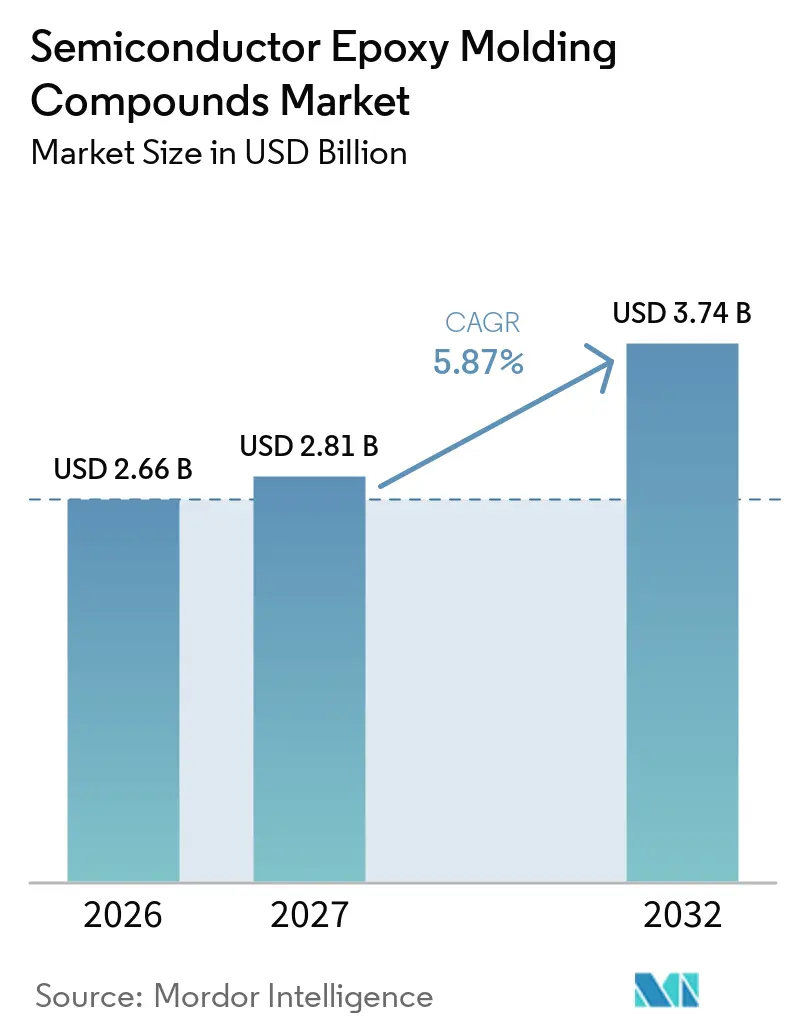
The Semiconductor Epoxy Molding Compounds Market size was valued at USD 2.66 billion in 2026 and is estimated to grow from USD 2.81 billion in 2027 to reach USD 3.74 billion by 2032, at a CAGR of 5.87% during the forecast period (2027-2032). Semiconductor epoxy molding compounds form the structural and environmental barrier around semiconductor dies, and their performance requirements rise as package designs combine more dies, denser interconnects, larger mold areas, and more demanding thermal conditions. Advanced packages use chiplets, 2.5D silicon interposers, fan-out wafer-level packages, and panel-level packages, requiring tighter control of warpage, coefficient of thermal expansion, heat resistance, flow behavior, curing behavior, and long-term interface reliability than standard transfer-mold grades provide. The shift from monolithic integrated circuits to multi-die assemblies, shaped by the slower gains from planar transistor scaling, is moving demand from commodity products toward tailored formulations and creating more pressure on suppliers that compete mainly on standard-grade materials. The semiconductor epoxy molding compounds market benefits from artificial intelligence infrastructure and vehicle electrification because large artificial intelligence packages, silicon carbide power modules, traction inverters, onboard chargers, and related systems require dependable encapsulation that can manage heat, stress, and dimensional change through assembly and use. This opportunity is tempered by multi-year qualification cycles, feedstock and high-purity filler costs, and design trade-offs among thermal expansion, moisture resistance, low stress, flowability, and warpage, all of which shape supplier investment, product development, customer switching decisions, and the relative value of established reliability data gathered across many package formats and end-use environments over extended qualification cycles.
Key Report Takeaways
- By type, high-temperature epoxy held 61.65% of the semiconductor epoxy molding compounds market share in 2026, while low-temperature epoxy is projected to advance at a 6.74% CAGR through 2032.
- By end-use industry, consumer electronics held 39.87% of the semiconductor epoxy molding compounds market share in 2026, while automotive electronics is projected to advance at a 7.08% CAGR through 2032.
- By geography, Asia-Pacific held 54.22% of the semiconductor epoxy molding compounds market share in 2026 and is projected to advance at a 6.81% CAGR through 2032.
Note: Market numbers in this report are based on Mordor Intelligence's proprietary estimation framework, which combines nine months of actuals with Q4 projections for base year 2026.
Global Semiconductor Epoxy Molding Compounds Market Trends and Insights
Drivers Impact Analysis*
| Driver | (~) % Impact on CAGR Forecast | Geographic Relevance | Impact Timeline |
|---|---|---|---|
| Advanced Packaging and Heterogeneous Integration | +1.8% | Global, concentrated in APAC core (Taiwan, South Korea, Japan) | Long term (≥ 4 years) |
| AI Accelerators, HPC and Data-Center Packaging | +1.5% | Global; APAC production, North America & EU demand | Medium term (2–4 years) |
| Automotive Electrification and Power-Semiconductor Reliability | +1.2% | Europe, APAC core, North America | Long term (≥ 4 years) |
| Low-Warpage Materials for Fan-Out and Panel-Level Packaging | +0.8% | APAC core; spillover to North America OSATs | Medium term (2–4 years) |
| Halogen-Free and Low-Alpha Encapsulation Requirements | +0.5% | Global, with regulatory influence particularly in EU and Japan | Short term (≤ 2 years) |
| Source: Mordor Intelligence | |||
Advanced Packaging and Heterogeneous Integration
The shift from monolithic chips to chiplet designs is changing the material requirements for the semiconductor epoxy molding compounds market. Fan-out redistribution layers embedded in molded substrates need compounds with coefficient of thermal expansion (CTE) values that closely match silicon. They also need flow behavior and curing characteristics suitable for much denser vertical interconnect structures. Samsung Semiconductor described how its heterogeneous integration platform used hybrid copper bonding for chiplet dies at a 9-10 µm pitch, a format that requires low-CTE encapsulation materials and balanced elastic properties[1]. Every added die creates more interfaces exposed to thermal stress, making long-term reliability a central selection factor for advanced packages.
AI Accelerators, HPC and Data-Center Packaging
Artificial intelligence accelerators and high-performance computing (HPC) packages are increasing the technical demands placed on the semiconductor epoxy molding compounds market. These packages combine multiple logic dies and high-bandwidth memory in a larger footprint, increasing heat generation, stress across the package, and the need for dimensional stability during assembly and operation. Advanced packaging has become a significant capacity constraint for artificial intelligence chips, rather than a secondary manufacturing step. The resulting demand supports compounds that maintain low warpage, controlled thermal expansion, reliable curing, and consistent performance under high thermal loads, particularly when packaging processes place fine-pitch structures close to sensitive interfaces. It also favors liquid compression mold compounds and other specialized formulations that can meet tighter dimensional tolerances than standard granular products. Suppliers with experience in low-stress material systems can strengthen their position by working with package makers on the compound, mold process, and reliability requirements together.
Automotive Electrification and Power-Semiconductor Reliability
Automotive electrification is expanding the use of power semiconductors in traction inverters, onboard chargers, and auxiliary power systems. These applications need encapsulants that can withstand repeated temperature changes and mechanical stress over long vehicle service lives. The semiconductor epoxy molding compounds market receives support from silicon carbide (SiC) and insulated-gate bipolar transistor (IGBT) modules, which operate under tougher conditions than many consumer packages. Sumitomo Bakelite Co., Ltd. began mass production of its SUMIKON EME-G785 Series in 2026 for next-generation SiC power modules. The compound has a glass transition temperature of 230 °C and was developed to combine heat resistance with low stress for high-output inverter applications.
Low-Warpage Materials for Fan-Out and Panel-Level Packaging
Panel-level fan-out packaging increases carrier dimensions to 320 mm × 320 mm and larger, making warpage harder to manage. Mismatched expansion among the compound, embedded dies, and process carrier can move a panel outside the process window. Higher filler content can reduce thermal expansion but can also reduce flowability, so particle size distribution becomes an important formulation decision. The semiconductor epoxy molding compounds market is, therefore, moving toward materials designed jointly with the panel process instead of grades adapted from wafer-level packaging.
Restraints Impact Analysis*
| Restraint | (~) % Impact on CAGR Forecast | Geographic Relevance | Impact Timeline |
|---|---|---|---|
| Long Qualification Cycles and Switching Costs | -0.9% | Global; most pronounced in automotive and aerospace | Long term (≥ 4 years) |
| CTE, Moisture and Warpage Trade-Offs | -0.7% | Global, concentrated in APAC advanced packaging hubs | Medium term (2–4 years) |
| Volatility in Epoxy Resin and High-Purity Filler Costs | -0.5% | Global; supply concentration risk in Japan for high-purity fillers | Short term (≤ 2 years) |
| Source: Mordor Intelligence | |||
Long Qualification Cycles and Switching Costs
Qualification cycles can slow the adoption of new materials in the semiconductor epoxy molding compounds market. Automotive and other high-reliability applications often require months of testing before a compound can be used in production. A material revision can require the customer to repeat qualification work, even if the change comes from the existing supplier. This makes customers cautious about moving to a new formulation or approving an additional supplier. It also means that material performance alone does not determine adoption speed. The first supplier to qualify a compound for a specific application can hold a strong position throughout the production life of that package.
CTE, Moisture and Warpage Trade-Offs
Formulators must balance thermal expansion, moisture resistance, mechanical stress, and flow behavior in a single encapsulant. A higher filler loading can reduce CTE and improve warpage control, but it may limit the material's ability to flow through a fine-pitch package. Lower stress can help protect fragile interfaces, while the resulting formulation must still meet heat resistance and process requirements. This trade-off adds development time for the semiconductor epoxy molding compounds market, especially in large fan-out and heterogeneous packages. The challenge is more pronounced when package dimensions increase or when several dies and substrate materials are combined. It prevents a simple formulation change from solving every package problem.
*Our forecasts treat driver/restraint impacts as directional, not additive. The impact forecasts reflect baseline growth, mix effects, and variable interactions.
Segment Analysis
By Type: High-Temperature Epoxy Sustains Dominance as Low-Temperature Epoxy Advances
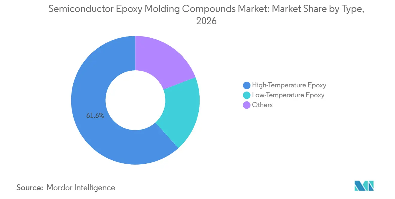
High-temperature epoxy held 61.65% of the semiconductor epoxy molding compounds market size in 2026. Its broad use across established package formats supported that leading position. Conventional quad flat packages and ball grid array packages can use high-temperature epoxy, as can thicker mold layers for discrete power devices. Existing transfer-mold equipment across the Asia-Pacific Outsourced Semiconductor Assembly and Test (OSAT) infrastructure also supports the continued use of this grade. Suppliers and package makers can rely on known processing windows and reliability behavior. This makes a shift to another material less attractive unless a new package requirement creates a clear advantage.
Low-temperature epoxy is projected to expand at a 6.74% CAGR through 2032. The growth reflects wider use of thermally sensitive components in heterogeneous packages, including embedded passive devices, optical interconnects, and organic interposers. These components may not tolerate standard 170–180 °C cure temperatures. Other materials, including liquid mold compounds and film-based encapsulants, are gaining use in fan-out wafer-level packaging and system-in-package designs. These alternatives can provide flow characteristics that granular compounds may not achieve in fine-pitch die arrays. The semiconductor epoxy molding compounds market is consequently serving both high-volume conventional packages and more specialized low-temperature or liquid applications.

By End-Use Industry: Consumer Electronics Anchors Scale, While Automotive Electronics Leads Growth
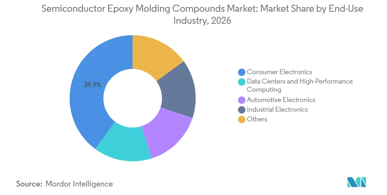
Consumer electronics held 39.87% of the semiconductor epoxy molding compounds market size in 2026. Smartphones, wearables, laptops, and tablets continued to create a large base of package demand. While smartphone shipments have plateaued, compound content per device can rise as application processors adopt system-in-package, package-on-package, and fan-out formats. These formats can require more encapsulant than legacy quad flat package or ball grid array designs. Consumer demand, therefore, remains important even where unit growth is limited. It also gives producers a large installed base for standard and intermediate-performance formulations.
Automotive electronics is projected to advance at a 7.08% CAGR through 2032, the highest rate among the stated end-use segments. Electric vehicles use several silicon carbide traction inverter modules and onboard charging systems that need high glass-transition-temperature and low-CTE encapsulants. Industrial electronics shares many of these requirements in motor drives, industrial inverters, and renewable energy converters. Data centers and high-performance computing use smaller unit volumes but can require the highest compound value per package because artificial intelligence accelerators are large and complex. The semiconductor epoxy molding compounds market gains from these applications because their package designs need low-stress liquid compression mold materials. Samsung SDI reported that its Materials Business revenue rose 14.5% year on year in the second quarter of 2026, while it expanded packaging-material partnerships into humanoid robotics and aerospace.
Geography Analysis
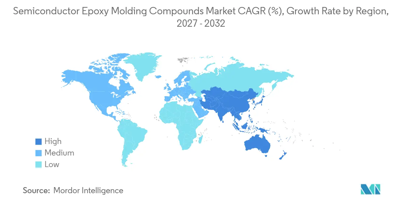
Asia-Pacific held 54.22% of the semiconductor epoxy molding compounds market size in 2026 and is projected to advance at a 6.81% CAGR through 2032. The region has a dense base of semiconductor assembly and testing activity in China, Japan, South Korea, and Taiwan. China is a major consumption center because it serves domestic artificial intelligence-chip packaging needs and supply-chain localization initiatives. Its capacity for commodity-grade compounds has expanded, while specialty grades still rely on suppliers with advanced formulation experience. Japan has a deep technical base in specialty epoxy molding compounds and high-purity silica fillers. This supplier network supports the broader global value chain as well as regional package makers.
South Korea's position is linked to its advanced packaging-material base and downstream integration. Samsung SDI and KCC Corporation are among the regional companies active in semiconductor materials. Samsung SDI's 2026 Materials Business performance reflected its push to broaden packaging-material relationships beyond mobile and memory applications. India remains a smaller consumer, but its announced semiconductor assembly investments make it a developing point of interest. Its present demand is still weighted toward lower-complexity package types. The semiconductor epoxy molding compounds market in Asia-Pacific remains closely connected to where large-scale assembly capacity and higher-value packaging development take place.
In North America, the United States drives demand for artificial intelligence accelerators, high-performance computing, hyperscale data centers, and defense electronics, even when assembly occurs in the Asia-Pacific. European demand is concentrated in Germany, France, and the United Kingdom, where automotive electronics producers need reliable power semiconductor modules. Henkel AG & Co. KGaA serves underfill and specialty encapsulant applications for European automotive and industrial original equipment manufacturers. South America and the Middle East and Africa remain smaller developing markets. Brazil's electronics assembly activity in Manaus supports conventional package demand, while Saudi Arabia's electronics manufacturing ambitions could create a longer-term pull for advanced packaging materials.
Competitive Landscape
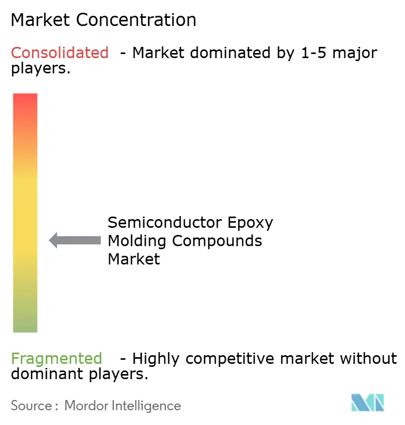
The semiconductor epoxy molding compounds market is moderately concentrated, with the top five players including Sumitomo Bakelite Co., Ltd., Resonac Holdings Corporation, Shin-Etsu Chemical Co., Ltd., KYOCERA Corporation, and SAMSUNG SDI. Japanese companies, including Sumitomo Bakelite Co., Ltd., Resonac Holdings Corporation, and Shin-Etsu Chemical Co., Ltd., have strong formulation experience and large reliability-data libraries built through long customer qualification histories. Taiwanese, South Korean, and Chinese producers compete more broadly across commodity and intermediate-grade materials, with several companies moving toward higher-value formulations as local packaging capability develops. The differences among suppliers extend beyond resin chemistry because reliable performance depends on filler quality, impurity control, package-specific process conditions, and the supplier's ability to support testing through the customer approval process.
Sumitomo Bakelite Co., Ltd. took steps in 2026 to strengthen its power-semiconductor materials position and started mass production of the SUMIKON EME-G785 Series for next-generation SiC power modules, bringing a 230 °C glass transition temperature to a solid epoxy formulation[2]. Resonac Holdings Corporation also reinforced its position in liquid encapsulants for advanced packages after its Japanese Patent No. 7687499 was upheld following a third-party opposition. These examples show how suppliers are using product development and intellectual property to protect positions in more demanding package applications. The semiconductor epoxy molding compounds market gives value to low-CTE, low-stress, and heat-resistant products that can be integrated into customer processes.
Mid-tier suppliers use geographic focus and collaboration to build their positions. KCC Corporation has presented epoxy molding compounds, active metal brazed ceramic substrates, and liquid molding compounds for power semiconductor applications in electric vehicles and artificial intelligence data centers. Nitto Denko Corporation and International Business Machines Corporation (IBM) entered a joint development agreement in September 2025 to work on advanced packaging materials for warpage control, thermal expansion management, and crosstalk reduction in high-density redistribution-layer interposers. The competitive opportunity remains strongest in ultra-low-CTE liquid compounds for glass interposer packages and thermally conductive materials for large-area power modules. These applications require a balanced combination of dimensional stability and thermal performance. They also give suppliers a reason to work more closely with package makers during process development.
Semiconductor Epoxy Molding Compounds Industry Leaders
-
Sumitomo Bakelite Co., Ltd.
-
Resonac Holdings Corporation
-
Shin-Etsu Chemical Co., Ltd.
-
KYOCERA Corporation
-
SAMSUNG SDI
- *Disclaimer: Major Players sorted in no particular order
Recent Industry Developments
- June 2026: Sumitomo Bakelite Co., Ltd. began mass production of its SUMIKON EME-G785 series, a high-glass transition temperature (Tg) epoxy molding compound for next-generation SiC power modules. The material achieves a Tg of 230 °C while maintaining low stress, supporting demand for high-temperature and reliable semiconductor encapsulation materials.
- April 2026: SP Samhwa commercialized and began mass production of Epoxy Molding Compound (EMC) after seven years of research and development, marking its expansion from paints into semiconductor materials. The development supports the semiconductor epoxy molding compounds market by adding production capacity for EMC used in semiconductor packaging and encapsulation.
Global Semiconductor Epoxy Molding Compounds Market Report Scope
Semiconductor epoxy molding compounds are thermosetting materials used to encapsulate and protect semiconductor devices from moisture, mechanical stress, contamination, and thermal effects. They provide electrical insulation and structural protection while supporting the reliability and durability of packaged semiconductor components.
The Semiconductor Epoxy Molding Compounds Market is segmented by type, end-use industry, and geography. By type, the market is segmented into high-temperature epoxy, low-temperature epoxy, and others. By end-use industry, the market is segmented into consumer electronics, automotive electronics, industrial electronics, data centers and high-performance computing, and others. The report also covers the market size and forecasts for semiconductor epoxy molding compounds across 15 countries. For each segment, the market sizing and forecasts have been done on the basis of value (USD).
| High-Temperature Epoxy |
| Low-Temperature Epoxy |
| Others |
| Consumer Electronics |
| Automotive Electronics |
| Industrial Electronics |
| Data Centers and High-Performance Computing |
| Others |
| Asia-Pacific | China |
| India | |
| Japan | |
| South Korea | |
| Rest of Asia-Pacific | |
| North America | United States |
| Canada | |
| Mexico | |
| Europe | Germany |
| United Kingdom | |
| France | |
| Italy | |
| Rest of Europe | |
| South America | Brazil |
| Argentina | |
| Rest of South America | |
| Middle East and Africa | Saudi Arabia |
| South Africa | |
| Rest of Middle East and Africa |
| By Type | High-Temperature Epoxy | |
| Low-Temperature Epoxy | ||
| Others | ||
| By End-Use Industry | Consumer Electronics | |
| Automotive Electronics | ||
| Industrial Electronics | ||
| Data Centers and High-Performance Computing | ||
| Others | ||
| By Geography | Asia-Pacific | China |
| India | ||
| Japan | ||
| South Korea | ||
| Rest of Asia-Pacific | ||
| North America | United States | |
| Canada | ||
| Mexico | ||
| Europe | Germany | |
| United Kingdom | ||
| France | ||
| Italy | ||
| Rest of Europe | ||
| South America | Brazil | |
| Argentina | ||
| Rest of South America | ||
| Middle East and Africa | Saudi Arabia | |
| South Africa | ||
| Rest of Middle East and Africa | ||
Key Questions Answered in the Report
What is the size of the semiconductor epoxy molding compounds market?
The Semiconductor Epoxy Molding Compounds Market size was valued at USD 2.66 billion in 2026 and is estimated to grow from USD 2.81 billion in 2027 to reach USD 3.74 billion by 2032, at a CAGR of 5.87% during the forecast period (2027-2032).
Which type held the largest share in 2026?
High-temperature epoxy held 61.65% share in 2026 because it is widely used across established package formats and transfer-mold processes.
Which end-use segment is expected to grow fastest through 2032?
Automotive electronics is projected to advance at a 7.08% CAGR through 2032, supported by electric-vehicle power modules and charging systems.
Why are advanced packages increasing encapsulant requirements?
Chiplets, fan-out formats, and 2.5D packages need tighter control of warpage, thermal expansion, flow behavior, and long-term reliability.