Semiconductor Die Inspection Imaging Systems Market Size and Share
Market Overview
| Study Period | 2020 - 2031 |
|---|---|
| Market Size (2026) | USD 2.03 Billion |
| Market Size (2031) | USD 3.61 Billion |
| Growth Rate (2026 - 2031) | 12.19 % |
| Fastest Growing Market | North America |
| Largest Market | Asia-Pacific |
| Market Concentration | Medium |
Major Players *Disclaimer: Major Players sorted in no particular order Image © Mordor Intelligence. Reuse requires attribution under CC BY 4.0. | |
Semiconductor Die Inspection Imaging Systems Market Analysis by Mordor Intelligence
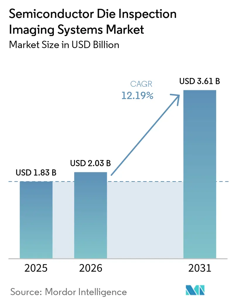
The semiconductor die inspection imaging systems market size is projected to expand from USD 1.83 billion in 2025 and USD 2.03 billion in 2026 to USD 3.61 billion by 2031, registering a CAGR of 12.19% between 2026 to 2031. Artificial intelligence infrastructure is sustaining capital spending on semiconductor equipment, which supports inspection and process-control demand. Smaller node geometries require manufacturers to use more than one inspection method across the production flow. Optical platforms remain important, but they cannot address every defect type at advanced nodes or inside stacked packages. Suppliers are moving from standalone tools toward connected process-control systems that combine inspection data with manufacturing feedback. New fabs supported by public programs and the growth of advanced packaging are widening the semiconductor die inspection imaging systems market opportunity.
Key Report Takeaways
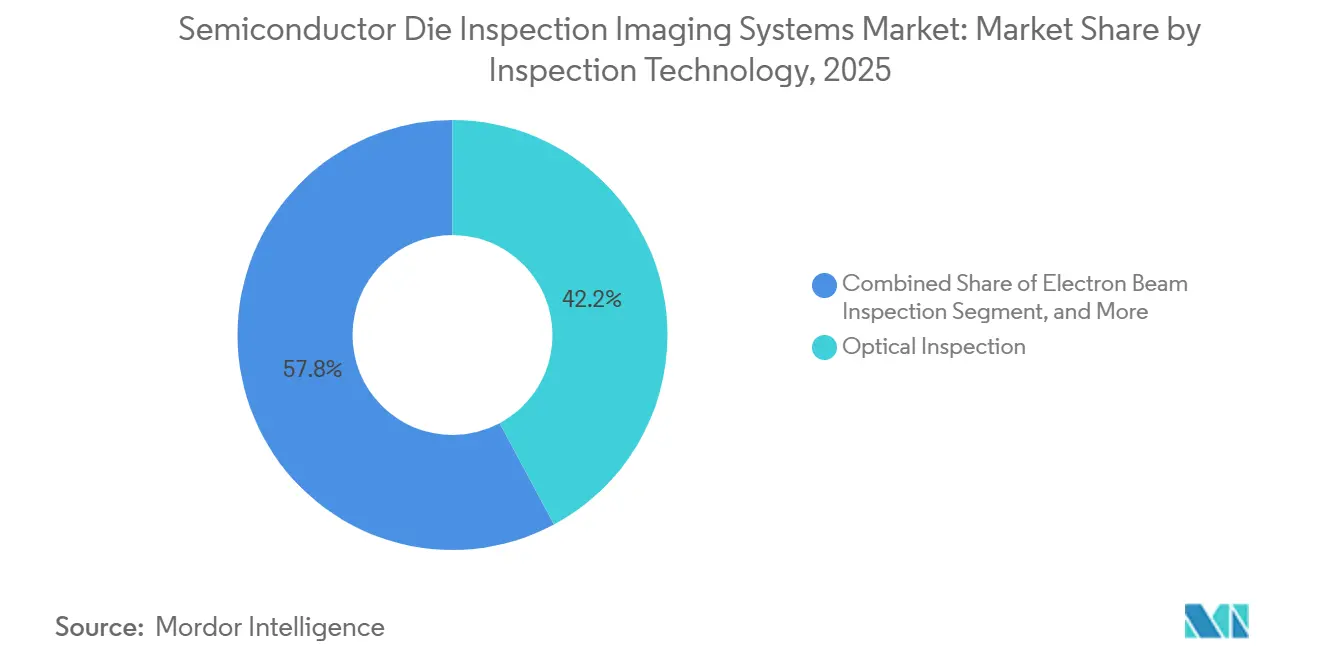
- By inspection technology, optical inspection held 42.18% of the semiconductor die inspection imaging systems market share in 2025, while X-ray inspection is projected to expand at a 14.23% CAGR through 2031.
- By inspection technique, two-dimensional imaging held 51.24% share in 2025, while three-dimensional imaging is projected to expand at a 14.76% CAGR through 2031.
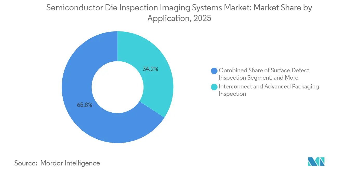
- By application, interconnect and advanced packaging inspection accounted for 34.16% of the semiconductor die inspection imaging systems market in 2025 and is projected to expand at a 15.64% CAGR through 2031.
- By end user, integrated device manufacturers held 36.12% share in 2025, while outsourced semiconductor assembly and test providers are projected to expand at a 15.13% CAGR through 2031.
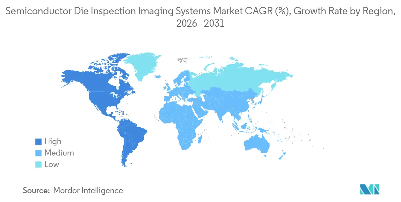
- By geography, Asia-Pacific held 58.27% share in the semiconductor die inspection imaging systems market in 2025, while North America is projected to expand at a 14.08% CAGR through 2031.
Note: Market size and forecast figures in this report are generated using Mordor Intelligence’s proprietary estimation framework, updated with the latest available data and insights as of January 2026.
Market Trends and Insights
Drivers Impact Analysis of Semiconductor Die Inspection Imaging Systems Market*
| DRIVER | (~) % IMPACT ON CAGR FORECAST | GEOGRAPHIC RELEVANCE | IMPACT TIMELINE |
|---|---|---|---|
| Rising Complexity of Advanced Semiconductor Nodes | +3.1% | Global, led by Taiwan, South Korea, and U.S. advanced logic fabs | Short term (≤ 2 years) |
| Expansion of Artificial Intelligence and High-Performance Computing Chip Production | +2.7% | Global, concentrated in Asia-Pacific foundries and U.S. hyperscaler supply chains | Short term (≤ 2 years) |
| Global Investments in New Semiconductor Fabrication Capacity | +2.0% | North America and Asia-Pacific, including Japan, India, and Southeast Asia | Medium term (2-4 years) |
| Increasing Adoption of Advanced Packaging and Heterogeneous Integration | +1.8% | Global, anchored in Taiwan CoWoS supply chains and South Korean HBM packaging | Medium term (2-4 years) |
| Intensifying Yield Improvement and Cost-of-Quality Requirements | +1.2% | Global, with the highest impact in advanced logic and memory fabs | Short term (≤ 2 years) |
| AI-Enabled Automated Defect Classification and Predictive Inspection | +0.9% | Global, with early deployment in North America and Taiwan | Long term (≥ 4 years) |
| Source: Mordor Intelligence | |||
Rising Complexity of Advanced Semiconductor Nodes
Gate-all-around transistor designs and backside power delivery increase the number and type of defects that must be identified during fabrication. These architectures use features that challenge the resolution limits of deep ultraviolet optical platforms. At nodes below 5nm, stochastic defects require denser wafer sampling because the events are probabilistic rather than systematic. This requirement raises tool utilization and increases inspection cost per wafer. Fabs therefore monitor more layers during production instead of relying mainly on end-of-line qualification. The semiconductor die inspection imaging systems market benefits as each process layer requires specific recipes for the node, layer, and tool model.
Expansion of Artificial Intelligence and High-Performance Computing Chip Production
AI accelerators are increasing the demand for inspection equipment because their advanced-node dies are larger than general-purpose processors. Larger dies create more inspection-sensitive sites on a wafer and increase the financial cost of a missed defect. High device value also makes yield loss more costly for foundries and their customers. These conditions encourage tighter sampling requirements across the manufacturing chain. Electron beam inspection is moving beyond research and sampling roles for critical layers where optical tools cannot resolve nanosheet edge roughness and stochastic EUV defects.
Global Investments in New Semiconductor Fabrication Capacity
The CHIPS and Science Act had allocated USD 38.7 billion of its USD 39 billion manufacturing incentive pool across 23 recipients by mid-2026. Around USD 11 billion had been disbursed against verified construction milestones, while 3 fabs were in production and 14 remained under construction. The projects represent added U.S. advanced and mature logic capacity expected to come online between 2026 and 2029. Each new fab requires inspection tools alongside deposition and other process equipment. The Section 48D investment tax credit applies to projects that begin construction by December 31, 2026, which can bring equipment orders forward. This investment cycle supports the semiconductor die inspection imaging systems market in North America and in regions expanding capacity for memory, logic, and specialty devices.[1]National Institute of Standards and Technology, “CHIPS for America,” National Institute of Standards and Technology, nist.gov.
Increasing Adoption of Advanced Packaging and Heterogeneous Integration
Advanced packaging is becoming necessary for AI and high-performance computing devices that use multiple dies and high-bandwidth memory. Conventional two-dimensional wafer inspection cannot identify all defects inside three-dimensional stacked structures. CoWoS, Foveros Direct 3D, and related approaches introduce micro-bump voids, copper-pad misalignment, and through-silicon-via fill variation within the package. These features require volumetric inspection rather than surface-only review. IBM Research reported that its Direct Bridge Multi-die package used 30μm-pitch micro-bump joints that passed 2,000 temperature-cycling test cycles, showing the demanding qualification environment around multi-die packaging. The semiconductor die inspection imaging systems market gains from the need to inspect structures from substrate fabrication through final package assembly.[2]Intel Corporation, “Foveros Direct 3D Technology Brief,” Intel, intel.com.
Restraints Impact Analysis of Semiconductor Die Inspection Imaging Systems Market*
| RESTRAINT | (~) % IMPACT ON CAGR FORECAST | GEOGRAPHIC RELEVANCE | IMPACT TIMELINE |
|---|---|---|---|
| High Capital Cost and Lengthy Qualification Cycles | -2.3% | Global, most acute in new-entrant fabs in North America and Europe | Medium term (2-4 years) |
| Shortage of Skilled Semiconductor Inspection Engineers | -1.5% | United States and Europe, moderating in Asia-Pacific through established university pipelines | Long term (≥ 4 years) |
| Multimodal Data Overload and Inspection Recipe Complexity | -0.8% | Global, with the highest impact in leading-edge logic fabs at 5nm and below | Medium term (2-4 years) |
| Hybrid-Bonding Defect Ambiguity and Cross-Tool Data Integration Challenges | -0.6% | Global, concentrated in Asia-Pacific advanced packaging hubs | Long term (≥ 4 years) |
| Source: Mordor Intelligence | |||
High Capital Cost and Lengthy Qualification Cycles
Electron beam inspection systems and advanced three-dimensional X-ray CT tools can cost USD 10 million to USD 15 million per unit. Qualification at a new fab can take 12 months to 18 months before a tool enters high-volume production. Large foundries and integrated device manufacturers can better absorb these timelines because they have established process-control teams and recipe libraries. Emerging fabs often have less engineering capacity to qualify tools quickly. This can concentrate equipment spending in a limited group of tier-1 facilities during the near term.
Shortage of Skilled Semiconductor Inspection Engineers
Inspection recipe development, defect model training, and cross-tool data correlation require specialized engineering skills. New hires can need 18 months to 36 months of on-the-job experience before they can undertake this work independently. The United States faces a projected shortage of 127,000 to 157,000 semiconductor and microelectronics workers by 2030 under optimistic assumptions. Engineers account for 60% of unmet demand, and 67,000 chip jobs could remain unfilled at current degree-completion rates. The National Network for Microelectronics Education and the SEMI Foundation expanded training initiatives in 2026, although program output will take time to reach fabs. Suppliers are responding by adding automated recipe generation and AI-guided defect triage to tool software.
*Our forecasts treat driver/restraint impacts as directional, not additive. The impact forecasts reflect baseline growth, mix effects, and variable interactions.
Semiconductor Die Inspection Imaging Systems Market Segment Analysis
By Inspection Technology:
Optical Platforms Retain Scale While X-Ray Demand BuildsOptical inspection held 42.18% of the semiconductor die inspection imaging systems market share in 2025. Its leading position reflects its high throughput in manufacturing settings that need full-wafer scans within minutes. Optical tools are used across both critical and noncritical layers because they support broad process-control coverage. Modern platforms also use AI-based classification to separate relevant defects from nuisance events. That capability reduces the electron beam review burden without requiring every tool to be replaced. The semiconductor die inspection imaging systems industry continues to depend on optical systems as the initial line of process control in high-volume fabs.
X-ray inspection is projected to expand at a 14.23% CAGR between 2026 and 2031. The semiconductor die inspection imaging systems market size for X-ray tools is supported by chip packages where micro-bumps, through-silicon vias, and hybrid copper bonds cannot be seen with optical methods. X-ray and computed tomography provide noncontact volumetric inspection for these structures. A 2026 technical study found that high-resolution three-dimensional X-ray nano-CT could analyze hybrid copper bonding at sub-micron resolution without sample preparation. ZEISS Semiconductor Manufacturing Technology developed its NLX platform for inline three-dimensional X-ray laminography at the 300mm wafer level. These tools show the shift from offline failure analysis to production-line inspection with automated process feedback.[3]Till Dreier, Daniel Nilsson, and Julius Hållstedt, “High-Resolution 3D X-Ray Imaging of Hybrid Bonding,” IEEE, ieee.org.



By Inspection Technique:
Two-Dimensional Systems Lead While Three-Dimensional Imaging ExpandsTwo-dimensional imaging held 51.24% share of the semiconductor die inspection imaging systems market size in 2025. The installed base remains broad because front-end wafer inspection largely relies on planar defect detection at high throughput. Two-dimensional systems support surface particle detection, patterned-wafer brightfield and darkfield inspection, and lithographic overlay verification. These process steps are required across nodes and fab generations. Computed tomography has a smaller revenue role but remains important for offline failure analysis and engineering qualification. It can reconstruct the full volume of a packaged device without sectioning, which supports root-cause work on multi-die assemblies.
Three-dimensional imaging is projected to expand at a 14.76% CAGR from 2026 to 2031. Volumetric chip structures change the practical definition of a defect because the relevant issue may sit below the accessible surface. ASML reported that its computational guided inspection approach improved defective die capture by up to 4.3 times on Micron Technology memory devices in production deployment. The platform combines machine learning with electron beam sampling and improves the use of existing tool fleets. Onto Innovation qualified its Dragonfly G5 for 2.5D advanced packaging and began customer shipments in June 2026. The tool provides dedicated three-dimensional macro-defect inspection and bump metrology for advanced packaging pitches.[4]ASML Holding N.V., “Computational Guided Dynamic Sampling E-Beam Inspection in High-Volume Manufacturing,” SPIE Proceedings, spiedigitallibrary.org.
By Application:
Advanced Packaging Becomes the Main Growth CenterInterconnect and advanced packaging inspection accounted for 34.16% of the semiconductor die inspection imaging systems market in 2025 and is projected to expand at a 15.64% CAGR through 2031. This category combines the largest application position with the highest growth rate in the semiconductor die inspection imaging systems market. Package-level defects in AI chip interconnects can have a significant effect on system yield. The category has moved from a back-end activity to a central inspection point in the manufacturing flow. Surface defect inspection remains a foundational application across wafer processing and die preparation. It continues to support equipment demand even as the growth center moves toward packaging-stage work.
Internal and structural defect inspection is becoming more relevant as hybrid bonding and direct copper-to-copper interconnects replace solder bump interfaces. It addresses subsurface voids, delamination, and buried interface failures that conventional surface inspection may not identify. Defect review and failure analysis has a smaller revenue contribution than inline inspection, but it remains important for manufacturing qualification. The move from wafer-level scanning electron microscope review toward package-level nano-CT analysis reflects the growing complexity of assembled devices. A 2026 study on CoWoS packaging described an AI-integrated design-of-experiment approach for improving inline X-ray compatibility during the design stage. The work indicates that academic and laboratory collaborations are contributing to application development alongside equipment vendors.
By End Users:
Integrated Device Manufacturers Lead and OSAT Providers AccelerateIntegrated device manufacturers held 36.12% share in 2025. Their position reflects their role as buyers of leading-edge inspection tools across front-end and back-end production flows. These companies combine design, fabrication, and packaging activities, which centralize inspection capital decisions. Their multi-year procurement programs support demand for high-value process-control platforms. Semiconductor foundries are also important buyers because AI chip designers and custom silicon programs require strict process-control standards. Research institutes and other semiconductor organizations have lower procurement volumes, but they help qualify inspection methods before commercial deployment.
Outsourced semiconductor assembly and test providers are projected to expand at a 15.13% CAGR from 2026 to 2031. Assembly work for heterogeneous integration is moving from captive integrated device manufacturer lines to specialist contract facilities. Chiplet packages require these providers to invest in three-dimensional imaging and X-ray systems that were previously concentrated in advanced foundries. Export Administration Regulations and the Commerce Control List affect which tools individual facilities can procure. This creates different levels of equipment access across the outsourced semiconductor assembly and test industry. Camtek reported FY2025 revenue of USD 496.1 million and stated that 2026 was expected to be a double-digit growth year, supported by Hawk-platform orders from integrated device manufacturers and outsourced semiconductor assembly and test providers for high-bandwidth memory and AI packaging.
Geography Analysis
APAC Semiconductor Die Inspection Imaging Systems Market
Asia-Pacific held 58.27% of the semiconductor die inspection imaging systems market share in 2025. The region hosts a substantial share of advanced logic and memory fabrication, which creates a large installed base for inspection tools. Taiwan and South Korea are particularly important because leading foundries and memory producers operate advanced manufacturing lines there. South Korea recorded semiconductor equipment spending of USD 21.5 billion in 2025, supported by DRAM and NAND expansion and the qualification of EUV-based memory manufacturing. Japan is also expanding its role in the supply chain through production and capacity projects in advanced processes. Tower Semiconductor announced a Japanese expansion for silicon photonics, silicon germanium, and advanced packaging in July 2026, with USD 1 billion in grants from Japan supporting the plan.[5]Tower Semiconductor, “Tower Semiconductor with METI Support Announces Strategic Capacity Expansion in Japan,” Tower Semiconductor, towersemi.com.
China and North America Semiconductor Die Inspection Imaging Systems Market
China continues to provide a distinct demand pool for mature-node inspection tools. Export controls constrain domestic activity at the most advanced nodes, but memory and mature-node activity in the Yangtze River Delta support equipment investment. Domestic Chinese suppliers are gaining technical capability in this part of the equipment base. The semiconductor die inspection imaging systems market in North America is projected to expand at a 14.08% CAGR through 2031. This growth is linked to the CHIPS Act incentive program and a pipeline of greenfield and expansion fab projects. Three CHIPS-supported fabs were in volume production by mid-2026, while 14 additional subsidized projects were under construction.
The Americas and EMEA Semiconductor Die Inspection Imaging Systems Market
U.S. logic manufacturing expansion raises the importance of yield improvement because domestic wafers face a reported 20% to 30% structural cost premium over equivalent Taiwan production. Inspection systems can help fabs address this cost pressure by identifying process issues earlier. Europe retains strategic importance through fab development in Germany and the Netherlands and through its inspection equipment and precision optics base. ASML’s metrology and inspection activities reinforce the region’s position in advanced process-control technology. South America, the Middle East, and Africa remained early-stage regions in 2026, with limited fabrication activity and demand centered on research institutes, specialty electronics producers, technology parks, and university facilities. These regions are expected to remain smaller contributors through 2031, although future sovereign manufacturing plans could alter their position after the forecast period.

Competitive Landscape
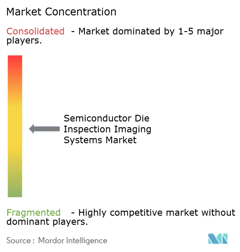
The semiconductor die inspection imaging systems market is moderately concentrated in leading-edge process control and more fragmented in specialty applications. KLA reported USD 13.58 billion in fiscal 2026 revenue, with USD 12.24 billion from its Semiconductor Process Control segment. Its order backlog reached USD 12.57 billion, compared with USD 7.86 billion a year earlier. These figures reflect sustained customer commitments connected to advanced manufacturing and AI infrastructure. KLA’s installed base, defect libraries, and integration within fab automation create meaningful barriers for suppliers seeking to displace established platforms.
ASML has a strong position in electron beam metrology and inspection through its HMI business. Lasertec holds a near-exclusive position in EUV mask blank inspection, which shows that individual niches can be highly concentrated even when the wider semiconductor die inspection imaging systems market is not. Onto Innovation completed a JPY 113 billion investment, equivalent to USD 720 million, for a 27% stake in Rigaku Holdings in August 2026. The investment expanded a strategic collaboration around X-ray process-control technologies for semiconductor manufacturing, advanced packaging, and three-dimensional integration. This move shows how suppliers are adding capabilities through investment and collaboration rather than relying only on internal development. Lasertec released the MATRICS X712 Series in March 2026 with redesigned optics, a new image-processing engine, and a 266nm in-house laser, supporting inspection for 5nm and below nodes.
Hybrid bonding inspection remains an open area because copper-to-copper bonds below 5μm pitch are difficult to classify automatically at production scale. This challenge can extend qualification schedules at advanced foundries. Machine-learning-assisted vision inspection also has room to move from pilot activity into certified high-volume use. The semiconductor die inspection imaging systems market favors vendors that can connect defect data across tool fleets, process steps, and fabs. Such data platforms can make a supplier more integrated with customer operations and increase switching costs. Onto Innovation’s Dragonfly G5 qualification and Rigaku investment illustrate the emphasis on advanced packaging and X-ray capability, while Lasertec’s new mask systems reflect ongoing work on EUV inspection.
Semiconductor Die Inspection Imaging Systems Industry Leaders
KLA Corporation
ASML Holding N.V.
Applied Materials, Inc.
Hitachi High-Tech Corporation
Onto Innovation Inc.
- *Disclaimer: Major Players sorted in no particular order
Semiconductor Die Inspection Imaging Systems Market Companies Covered in this Report
- KLA Corporation
- ASML Holding N.V.
- Applied Materials, Inc.
- Hitachi High-Tech Corporation
- Onto Innovation Inc.
- Camtek Ltd.
- Nova Ltd.
- Lasertec Corporation
- JEOL Ltd.
- Toray Engineering Co., Ltd.
- SCREEN Semiconductor Solutions Co., Ltd.
- Tokyo Electron Limited
- Advantest Corporation
- Veeco Instruments Inc.
- Nordson Corporation
- Thermo Fisher Scientific Inc.
- HORIBA, Ltd.
- Nikon Corporation
- Bruker Corporation
- Carl Zeiss AG
- Nextin Inc.
- Photo Electron Soul Inc.
- PEMTRON Co., Ltd.
- Koh Young Technology Inc.
- MUETEC Co., Ltd.
- ViTrox Corporation Berhad
- Confovis GmbH
- SAKI Corporation
- Machine Vision Products, Inc.
- Advanced Spectral Technology, Inc.
- ISRA VISION GmbH
- CIMS Co., Ltd.

Recent Industry Developments in Semiconductor Die Inspection Imaging Systems Market
- August 2026: Onto Innovation Inc. completed its acquisition of a 27% minority equity stake in Rigaku Holdings Corporation from Atom Investment, a Carlyle affiliate, for JPY 113 billion (USD 720 million). The investment deepened a strategic collaboration first announced in April 2026 to advance X-ray-based process-control technologies for semiconductor manufacturing applications, including advanced packaging and 3D integration. It broadened Onto Innovation’s access to X-ray process-control technologies for the semiconductor die inspection imaging systems market.
- August 2026: SK Hynix's board approved KRW 54 trillion (USD 38.3 billion) for 2 new semiconductor fabs. The Yongin Y2 DRAM facility received KRW 35.2 trillion and the Cheongju M17 NAND fab received KRW 19.1 trillion. M17 is expected to break ground in February 2027 and Y2 in July 2027. The capacity projects create a major forward demand signal for advanced inspection equipment across memory production.
- July 2026: Tower Semiconductor announced a dual-track capacity expansion in Japan for silicon photonics, silicon germanium, and advanced packaging. Tower projected investment of USD 3 billion net of USD 1 billion in grants from the Government of Japan under METI’s semiconductor revitalization initiative. The plan links process expansion with the equipment requirements of specialty manufacturing and advanced packaging. Those requirements include process-control and inspection capacity across the planned production flows.
- June 2026: Applied Materials introduced the Centris Spectral SiN ALD and Producer Selectra Mo Etch systems for advanced 3D chip scaling. The systems are designed to provide precision processing in deep and narrow three-dimensional structures for logic and memory devices. Their stated purpose is to address yield improvement requirements at advanced nodes. The release reflects the wider emphasis on managing variation in complex device structures.


Global Semiconductor Die Inspection Imaging Systems Market Report Scope
The Semiconductor Die Inspection Imaging Systems Market comprises high-resolution optical, electron-beam, and X-ray imaging equipment used to detect surface and subsurface defects, measure critical dimensions, and verify structural integrity on individual semiconductor dies during and after fabrication. These systems employ advanced imaging technologies including brightfield/darkfield optics, scanning electron microscopy (SEM), automated optical inspection (AOI), and AI-enhanced image analysis to identify particles, pattern defects, cracks, voids, and metallization anomalies at nanometer-scale resolution, enabling manufacturers to maintain yield rates, reduce scrap, and ensure quality compliance as device geometries shrink and packaging densities increase for logic, memory, and advanced packaging applications.
The Semiconductor Die Inspection Imaging Systems Market Report is Segmented by Inspection Technology (Optical Inspection, X-Ray Inspection, Electron Beam Inspection, and Ultraviolet, Infrared, and Multispectral Inspection), Inspection Technique (Two-Dimensional Imaging, Three-Dimensional Imaging, and Computed Tomography Imaging), Application (Surface Defect Inspection, Internal and Structural Defect Inspection, Interconnect and Advanced Packaging Inspection, and Defect Review and Failure Analysis), End-Users (Integrated Device Manufacturers, Semiconductor Foundries, Outsourced Semiconductor Assembly and Test Providers, and Research Institutes and Other Semiconductor Organizations), and Geography (North America, South America, Europe, Asia-Pacific, and Middle East and Africa). The Market Forecasts are Provided in Terms of Value (USD).
| Optical Inspection |
| X-Ray Inspection |
| Electron Beam Inspection |
| Ultraviolet, Infrared, and Multispectral Inspection |
| Two-Dimensional Imaging |
| Three-Dimensional Imaging |
| Computed Tomography Imaging |
| Surface Defect Inspection |
| Internal and Structural Defect Inspection |
| Interconnect and Advanced Packaging Inspection |
| Defect Review and Failure Analysis |
| Integrated Device Manufacturers |
| Semiconductor Foundries |
| Outsourced Semiconductor Assembly and Test Providers |
| Research Institutes and Other Semiconductor Organizations |
| North America | United States | |
| Canada | ||
| Mexico | ||
| South America | Brazil | |
| Argentina | ||
| Rest of South America | ||
| Europe | Germany | |
| United Kingdom | ||
| France | ||
| Italy | ||
| Spain | ||
| Rest of Europe | ||
| Asia-Pacific | China | |
| Japan | ||
| India | ||
| South Korea | ||
| ASEAN | ||
| Rest of Asia-Pacific | ||
| Middle East and Africa | Middle East | Saudi Arabia |
| United Arab Emirates | ||
| Turkey | ||
| Rest of the Middle East | ||
| Africa | South Africa | |
| Nigeria | ||
| Rest of Africa | ||
| By Inspection Technology | Optical Inspection | ||
| X-Ray Inspection | |||
| Electron Beam Inspection | |||
| Ultraviolet, Infrared, and Multispectral Inspection | |||
| By Inspection Technique | Two-Dimensional Imaging | ||
| Three-Dimensional Imaging | |||
| Computed Tomography Imaging | |||
| By Application | Surface Defect Inspection | ||
| Internal and Structural Defect Inspection | |||
| Interconnect and Advanced Packaging Inspection | |||
| Defect Review and Failure Analysis | |||
| By End-Users | Integrated Device Manufacturers | ||
| Semiconductor Foundries | |||
| Outsourced Semiconductor Assembly and Test Providers | |||
| Research Institutes and Other Semiconductor Organizations | |||
| By Geography | North America | United States | |
| Canada | |||
| Mexico | |||
| South America | Brazil | ||
| Argentina | |||
| Rest of South America | |||
| Europe | Germany | ||
| United Kingdom | |||
| France | |||
| Italy | |||
| Spain | |||
| Rest of Europe | |||
| Asia-Pacific | China | ||
| Japan | |||
| India | |||
| South Korea | |||
| ASEAN | |||
| Rest of Asia-Pacific | |||
| Middle East and Africa | Middle East | Saudi Arabia | |
| United Arab Emirates | |||
| Turkey | |||
| Rest of the Middle East | |||
| Africa | South Africa | ||
| Nigeria | |||
| Rest of Africa | |||


Key Questions Answered in the Report
What is the semiconductor die inspection imaging systems market size?
The semiconductor die inspection imaging systems market size is projected to expand from USD 1.83 billion in 2025 and USD 2.03 billion in 2026 to USD 3.61 billion by 2031, registering a CAGR of 12.19% between 2026 to 2031.
What is driving demand for semiconductor die inspection imaging systems?
Advanced nodes, AI and high-performance computing chips, new fab construction, and advanced packaging are increasing inspection requirements.
Which inspection technology leads semiconductor die inspection imaging systems?
Optical inspection led with 42.18% share in 2025 because it provides high-throughput full-wafer process control.
Which imaging technique is growing the fastest?
Three-dimensional imaging is projected to expand at a 14.76% CAGR through 2031 as more devices use stacked and volumetric structures.
Which application has the strongest growth outlook?
Interconnect and advanced packaging inspection held 34.16% share in 2025 and is projected to expand at a 15.64% CAGR through 2031.
Which region has the largest semiconductor die inspection imaging systems demand?
Asia-Pacific held 58.27% share in 2025, while North America is projected to grow at a 14.08% CAGR through 2031.
Page last updated on: